

Chemical vapor deposition
Encyclopedia
Chemical process
In a "scientific" sense, a chemical process is a method or means of somehow changing one or more chemicals or chemical compounds. Such a chemical process can occur by itself or be caused by somebody. Such a chemical process commonly involves a chemical reaction of some sort...
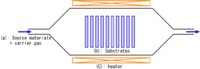
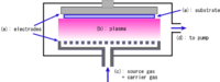
used to produce high-purity, high-performance solid materials. The process is often used in the semiconductor industry
Semiconductor industry
The semiconductor industry is the aggregate collection of companies engaged in the design and fabrication of semiconductor devices. It formed around 1960, once the fabrication of semiconductors became a viable business...
to produce thin film
Thin film
A thin film is a layer of material ranging from fractions of a nanometer to several micrometers in thickness. Electronic semiconductor devices and optical coatings are the main applications benefiting from thin film construction....
s. In a typical CVD process, the wafer
Wafer (electronics)
A wafer is a thin slice of semiconductor material, such as a silicon crystal, used in the fabrication of integrated circuits and other microdevices...
(substrate) is exposed to one or more volatile
Volatility (chemistry)
In chemistry and physics, volatility is the tendency of a substance to vaporize. Volatility is directly related to a substance's vapor pressure. At a given temperature, a substance with higher vapor pressure vaporizes more readily than a substance with a lower vapor pressure.The term is primarily...
precursors, which react
Chemical reaction
A chemical reaction is a process that leads to the transformation of one set of chemical substances to another. Chemical reactions can be either spontaneous, requiring no input of energy, or non-spontaneous, typically following the input of some type of energy, such as heat, light or electricity...
and/or decompose
Chemical decomposition
Chemical decomposition, analysis or breakdown is the separation of a chemical compound into elements or simpler compounds. It is sometimes defined as the exact opposite of a chemical synthesis. Chemical decomposition is often an undesired chemical reaction...
on the substrate surface to produce the desired deposit. Frequently, volatile by-product
By-product
A by-product is a secondary product derived from a manufacturing process or chemical reaction. It is not the primary product or service being produced.A by-product can be useful and marketable or it can be considered waste....
s are also produced, which are removed by gas flow through the reaction chamber.
Microfabrication
Microfabrication
Microfabrication is the term that describes processes of fabrication of miniature structures, of micrometre sizes and smaller. Historically the earliest microfabrication processes were used for integrated circuit fabrication, also known as "semiconductor manufacturing" or "semiconductor device...
processes widely use CVD to deposit materials in various forms, including: monocrystalline, polycrystalline
Polycrystalline
Polycrystalline materials are solids that are composed of many crystallites of varying size and orientation. The variation in direction can be random or directed, possibly due to growth and processing conditions. Fiber texture is an example of the latter.Almost all common metals, and many ceramics...
, amorphous, and epitaxial
Epitaxy
Epitaxy refers to the deposition of a crystalline overlayer on a crystalline substrate, where the overlayer is in registry with the substrate. In other words, there must be one or more preferred orientations of the overlayer with respect to the substrate for this to be termed epitaxial growth. The...
. These materials include: silicon
Silicon
Silicon is a chemical element with the symbol Si and atomic number 14. A tetravalent metalloid, it is less reactive than its chemical analog carbon, the nonmetal directly above it in the periodic table, but more reactive than germanium, the metalloid directly below it in the table...
, carbon fiber, carbon nanofibers, filaments, carbon nanotube
Carbon nanotube
Carbon nanotubes are allotropes of carbon with a cylindrical nanostructure. Nanotubes have been constructed with length-to-diameter ratio of up to 132,000,000:1, significantly larger than for any other material...
s, SiO2
Silicon dioxide
The chemical compound silicon dioxide, also known as silica , is an oxide of silicon with the chemical formula '. It has been known for its hardness since antiquity...
, silicon-germanium, tungsten
Tungsten
Tungsten , also known as wolfram , is a chemical element with the chemical symbol W and atomic number 74.A hard, rare metal under standard conditions when uncombined, tungsten is found naturally on Earth only in chemical compounds. It was identified as a new element in 1781, and first isolated as...
, silicon carbide
Silicon carbide
Silicon carbide , also known as carborundum, is a compound of silicon and carbon with chemical formula SiC. It occurs in nature as the extremely rare mineral moissanite. Silicon carbide powder has been mass-produced since 1893 for use as an abrasive...
, silicon nitride
Silicon nitride
Silicon nitride is a chemical compound of silicon and nitrogen. If powdered silicon is heated between 1300° and 1400°C in an atmosphere of nitrogen, trisilicon tetranitride, Si3N4, is formed. The silicon sample weight increases progressively due to the chemical combination of silicon and nitrogen...
, silicon oxynitride
Silicon oxynitride
Silicon oxynitride is a ceramic material with the chemical formula SiOxNy. While in amorphous forms its composition can continuously vary between SiO2 and Si3N4 , the only known intermediate crystalline phase is Si2N2O...
, titanium nitride
Titanium nitride
Titanium nitride is an extremely hard ceramic material, often used as a coating on titanium alloys, steel, carbide, and aluminium components to improve the substrate's surface properties....
, and various high-k dielectric
High-k Dielectric
The term high-κ dielectric refers to a material with a high dielectric constant κ used in semiconductor manufacturing processes which replaces the silicon dioxide gate dielectric...
s. The CVD process is also used to produce synthetic diamond
Synthetic diamond
Synthetic diamond is diamond produced in a technological process; as opposed to natural diamond, which is created in geological processes. Synthetic diamond is also widely known as HPHT diamond or CVD diamond, denoting the production method, High-Pressure High-Temperature synthesis and Chemical...
s.
Types of chemical vapor deposition
- Classified by operating pressure
- Atmospheric pressure CVD (APCVD) – CVD processes at atmospheric pressure.
- Low-pressure CVD (LPCVD) – CVD processes at subatmospheric pressures. Reduced pressures tend to reduce unwanted gas-phase reactions and improve film uniformity across the wafer. Most modern CVD processes are either LPCVD or UHVCVD.
- Ultrahigh vacuum CVD (UHVCVD) – CVD processes at a very low pressure, typically below 10−6 PaPascal (unit)The pascal is the SI derived unit of pressure, internal pressure, stress, Young's modulus and tensile strength, named after the French mathematician, physicist, inventor, writer, and philosopher Blaise Pascal. It is a measure of force per unit area, defined as one newton per square metre...
(~10−8 torrTorrThe torr is a non-SI unit of pressure with the ratio of 760 to 1 standard atmosphere, chosen to be roughly equal to the fluid pressure exerted by a millimetre of mercury, i.e., a pressure of 1 torr is approximately equal to 1 mmHg...
). Note that in other fields, a lower division between high and ultra-high vacuum is common, often 10−7 Pa.
- Classified by physical characteristics of vapor
- Aerosol assisted CVD (AACVD) – A CVD process in which the precursors are transported to the substrate by means of a liquid/gas aerosol, which can be generated ultrasonically. This technique is suitable for use with non-volatile precursors.
- Direct liquid injection CVD (DLICVD) – A CVD process in which the precursors are in liquid form (liquid or solid dissolved in a convenient solvent). Liquid solutions are injected in a vaporization chamber towards injectors (typically car injectors). Then the precursor vapors are transported to the substrate as in classical CVD process. This technique is suitable for use on liquid or solid precursors. High growth rates can be reached using this technique.
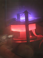
- Plasma methods (see also Plasma processingPlasma processingPlasma processing is a plasma-based material processing technology that aims at modifying the chemical and physical properties of a surface.Plasma processing techniques include:*Plasma activation*Plasma etching*Plasma modification*Plasma functionalization...
)- Microwave plasma-assisted CVD (MPCVD)
- Plasma-Enhanced CVDPlasma-enhanced chemical vapor depositionPlasma-enhanced chemical vapor deposition is a process used to deposit thin films from a gas state to a solid state on a substrate. Chemical reactions are involved in the process, which occur after creation of a plasma of the reacting gases...
(PECVD) – CVD processes that utilize plasmaPlasma (physics)In physics and chemistry, plasma is a state of matter similar to gas in which a certain portion of the particles are ionized. Heating a gas may ionize its molecules or atoms , thus turning it into a plasma, which contains charged particles: positive ions and negative electrons or ions...
to enhance chemical reaction rates of the precursors. PECVD processing allows deposition at lower temperatures, which is often critical in the manufacture of semiconductors. - Remote plasma-enhanced CVD (RPECVD) – Similar to PECVD except that the wafer substrate is not directly in the plasma discharge region. Removing the wafer from the plasma region allows processing temperatures down to room temperature.
- Atomic layer CVD (ALCVD) – Deposits successive layers of different substances to produce layered, crystalCrystalA crystal or crystalline solid is a solid material whose constituent atoms, molecules, or ions are arranged in an orderly repeating pattern extending in all three spatial dimensions. The scientific study of crystals and crystal formation is known as crystallography...
line films. See Atomic layer epitaxyAtomic layer epitaxyAtomic layer epitaxy or Atomic Layer Chemical Vapor Deposition , now more generally called Atomic Layer Deposition , is a specialized form of epitaxy that typically deposit alternating monolayers of two elements onto a substrate. The crystal lattice structure achieved is thin, uniform, and...
. - Combustion Chemical Vapor DepositionCombustion chemical vapor depositionCombustion chemical vapor deposition is a chemical process by which thin film coatings are deposited onto substrates in the open atmosphere.- History :...
(CCVD) – nGimat's proprietary Combustion Chemical Vapor Deposition process is an open-atmosphere, flame-based technique for depositing high-quality thin films and nanomaterials. - Hot wire CVD (HWCVD) – also known as catalytic CVD (Cat-CVD) or hot filament CVD (HFCVD). Uses a hot filament to chemically decompose the source gases.
- Metalorganic chemical vapor deposition (MOCVD) – CVD processes based on metalorganic precursors.
- Hybrid Physical-Chemical Vapor DepositionHybrid Physical-Chemical Vapor DepositionHybrid physical-chemical vapor deposition is a thin-film deposition technique that combines physical vapor deposition with chemical vapor deposition...
(HPCVD) – Vapor deposition processes that involve both chemical decomposition of precursor gas and vaporizationVaporizationVaporization of an element or compound is a phase transition from the liquid or solid phase to gas phase. There are three types of vaporization: evaporation, boiling and sublimation....
of a solid source. - Rapid thermal CVD (RTCVD) – CVD processes that use heating lamps or other methods to rapidly heat the wafer substrate. Heating only the substrate rather than the gas or chamber walls helps reduce unwanted gas phase reactions that can lead to particleParticle (ecology)In marine and freshwater ecology, a particle is a small object. Particles can remain in suspension in the ocean or freshwater, however they eventually settle and accumulate as sediment. Some can enter the atmosphere through wave action where they can act as cloud condensation nuclei...
formation. - Vapor phase epitaxy (VPE)
Substances commonly deposited for ICs
This section discusses the CVD processes often used for integrated circuits (ICs). Particular materials are deposited best under particular conditions.Polysilicon
Polycrystalline silicon is deposited from silaneSilane
Silane is a toxic, extremely flammable chemical compound with chemical formula SiH4. In 1857, the German chemists and Friedrich Woehler discovered silane among the products formed by the action of hydrochloric acid on aluminum silicide, which they had previously prepared...
(SiH4), using the following reaction:
- SiH4 → Si + 2 H2
This reaction is usually performed in LPCVD systems, with either pure silane feedstock, or a solution of silane with 70–80% nitrogen
Nitrogen
Nitrogen is a chemical element that has the symbol N, atomic number of 7 and atomic mass 14.00674 u. Elemental nitrogen is a colorless, odorless, tasteless, and mostly inert diatomic gas at standard conditions, constituting 78.08% by volume of Earth's atmosphere...
. Temperatures between 600 and 650 °C and pressures between 25 and 150 Pa yield a growth rate between 10 and 20 nm
Nanometre
A nanometre is a unit of length in the metric system, equal to one billionth of a metre. The name combines the SI prefix nano- with the parent unit name metre .The nanometre is often used to express dimensions on the atomic scale: the diameter...
per minute. An alternative process uses a hydrogen
Hydrogen
Hydrogen is the chemical element with atomic number 1. It is represented by the symbol H. With an average atomic weight of , hydrogen is the lightest and most abundant chemical element, constituting roughly 75% of the Universe's chemical elemental mass. Stars in the main sequence are mainly...
-based solution. The hydrogen reduces the growth rate, but the temperature is raised to 850 or even 1050 °C to compensate.
Polysilicon may be grown directly with doping, if gases such as phosphine
Phosphine
Phosphine is the compound with the chemical formula PH3. It is a colorless, flammable, toxic gas. Pure phosphine is odourless, but technical grade samples have a highly unpleasant odor like garlic or rotting fish, due to the presence of substituted phosphine and diphosphine...
, arsine
Arsine
Arsine is the chemical compound with the formula AsH3. This flammable, pyrophoric, and highly toxic gas is one of the simplest compounds of arsenic...
or diborane
Diborane
Diborane is the chemical compound consisting of boron and hydrogen with the formula B2H6. It is a colorless gas at room temperature with a repulsively sweet odor. Diborane mixes well with air, easily forming explosive mixtures. Diborane will ignite spontaneously in moist air at room temperature...
are added to the CVD chamber. Diborane increases the growth rate, but arsine and phosphine decrease it.
Silicon dioxide
Silicon dioxide (usually called simply "oxide" in the semiconductor industry) may be deposited by several different processes. Common source gases include silaneSilane
Silane is a toxic, extremely flammable chemical compound with chemical formula SiH4. In 1857, the German chemists and Friedrich Woehler discovered silane among the products formed by the action of hydrochloric acid on aluminum silicide, which they had previously prepared...
and oxygen
Oxygen
Oxygen is the element with atomic number 8 and represented by the symbol O. Its name derives from the Greek roots ὀξύς and -γενής , because at the time of naming, it was mistakenly thought that all acids required oxygen in their composition...
, dichlorosilane
Dichlorosilane
Dichlorosilane , or DCS as it is commonly known, is usually mixed with ammonia in LPCVD chambers to grow silicon nitride in semiconductor processing.A higher concentration of DCS:NH3 Dichlorosilane (H2SiCl2), or DCS as it is commonly known, is usually mixed with ammonia (NH3) in LPCVD chambers to...
(SiCl2H2) and nitrous oxide
Nitrous oxide
Nitrous oxide, commonly known as laughing gas or sweet air, is a chemical compound with the formula . It is an oxide of nitrogen. At room temperature, it is a colorless non-flammable gas, with a slightly sweet odor and taste. It is used in surgery and dentistry for its anesthetic and analgesic...
(N2O), or tetraethylorthosilicate (TEOS; Si(OC2H5)4). The reactions are as follows :
- SiH4 + O2 → SiO2 + 2 H2
- SiCl2H2 + 2 N2O → SiO2 + 2 N2 + 2 HCl
- Si(OC2H5)4 → SiO2 + byproducts
The choice of source gas depends on the thermal stability of the substrate; for instance, aluminium
Aluminium
Aluminium or aluminum is a silvery white member of the boron group of chemical elements. It has the symbol Al, and its atomic number is 13. It is not soluble in water under normal circumstances....
is sensitive to high temperature. Silane deposits between 300 and 500 °C, dichlorosilane at around 900 °C, and TEOS between 650 and 750 °C, resulting in a layer of low- temperature oxide (LTO). However, silane produces a lower-quality oxide than the other methods (lower dielectric strength
Dielectric strength
In physics, the term dielectric strength has the following meanings:*Of an insulating material, the maximum electric field strength that it can withstand intrinsically without breaking down, i.e., without experiencing failure of its insulating properties....
, for instance), and it deposits nonconformally
Conformal film
A conformal film defines a morphologically uneven interface with another body and has a thickness that is the same everywhere along the interface. This is undoubtedly an idealization and may be used for abstract or theoretical purposes...
. Any of these reactions may be used in LPCVD, but the silane reaction is also done in APCVD. CVD oxide invariably has lower quality than thermal oxide
Thermal oxidation
In microfabrication, thermal oxidation is a way to produce a thin layer of oxide on the surface of a wafer. The technique forces an oxidizing agent to diffuse into the wafer at high temperature and react with it. The rate of oxide growth is often predicted by the Deal-Grove model...
, but thermal oxidation can only be used in the earliest stages of IC manufacturing.
Oxide may also be grown with impurities (alloy
Alloy
An alloy is a mixture or metallic solid solution composed of two or more elements. Complete solid solution alloys give single solid phase microstructure, while partial solutions give two or more phases that may or may not be homogeneous in distribution, depending on thermal history...
ing or "doping
Doping (semiconductor)
In semiconductor production, doping intentionally introduces impurities into an extremely pure semiconductor for the purpose of modulating its electrical properties. The impurities are dependent upon the type of semiconductor. Lightly and moderately doped semiconductors are referred to as extrinsic...
"). This may have two purposes. During further process steps that occur at high temperature, the impurities may diffuse
Atomic diffusion
Atomic diffusion is a diffusion process whereby the random thermally-activated movement of atoms in a solid results in the net transport of atoms. For example, helium atoms inside a balloon can diffuse through the wall of the balloon and escape, resulting in the balloon slowly deflating. Other air...
from the oxide into adjacent layers (most notably silicon) and dope them. Oxides containing 5–15% impurities by mass are often used for this purpose. In addition, silicon dioxide alloyed with phosphorus pentoxide
Phosphorus pentoxide
Phosphorus pentoxide is a chemical compound with molecular formula P4O10 . This white crystalline solid is the anhydride of phosphoric acid. It is a powerful desiccant.-Structure:...
("P-glass") can be used to smooth out uneven surfaces. P-glass softens and reflows at temperatures above 1000 °C. This process requires a phosphorus concentration of at least 6%, but concentrations above 8% can corrode aluminium. Phosphorus is deposited from phosphine gas and oxygen:
- 4 PH3 + 5 O2 → 2 P2O5 + 6 H2
Glass
Glass
Glass is an amorphous solid material. Glasses are typically brittle and optically transparent.The most familiar type of glass, used for centuries in windows and drinking vessels, is soda-lime glass, composed of about 75% silica plus Na2O, CaO, and several minor additives...
es containing both boron and phosphorus (borophosphosilicate glass, BPSG) undergo viscous flow at lower temperatures; around 850 °C is achievable with glasses containing around 5 weight % of both constituents, but stability in air can be difficult to achieve. Phosphorus oxide in high concentrations interacts with ambient moisture to produce phosphoric acid. Crystals of BPO4 can also precipitate from the flowing glass on cooling; these crystals are not readily etched in the standard reactive plasmas used to pattern oxides, and will result in circuit defects in integrated circuit manufacturing.
Besides these intentional impurities, CVD oxide may contain byproducts of the deposition process. TEOS produces a relatively pure oxide, whereas silane introduces hydrogen impurities, and dichlorosilane introduces chlorine
Chlorine
Chlorine is the chemical element with atomic number 17 and symbol Cl. It is the second lightest halogen, found in the periodic table in group 17. The element forms diatomic molecules under standard conditions, called dichlorine...
.
Lower temperature deposition of silicon dioxide and doped glasses from TEOS using ozone rather than oxygen has also been explored (350 to 500 °C). Ozone glasses have excellent conformality but tend to be hygroscopic – that is, they absorb water from the air due to the incorporation of silanol (Si-OH) in the glass. Infrared spectroscopy and mechanical strain as a function of temperature are valuable diagnostic tools for diagnosing such problems.
Silicon nitride
Silicon nitride is often used as an insulator and chemical barrier in manufacturing ICs. The following two reactions deposit nitride from the gas phase:- 3 SiH4 + 4 NH3 → Si3N4 + 12 H2
- 3 SiCl2H2 + 4 NH3 → Si3N4 + 6 HCl + 6 H2
Silicon nitride deposited by LPCVD contains up to 8% hydrogen. It also experiences strong tensile stress
Stress (physics)
In continuum mechanics, stress is a measure of the internal forces acting within a deformable body. Quantitatively, it is a measure of the average force per unit area of a surface within the body on which internal forces act. These internal forces are a reaction to external forces applied on the body...
, which may crack films thicker than 200 nm. However, it has higher resistivity
Resistivity
Electrical resistivity is a measure of how strongly a material opposes the flow of electric current. A low resistivity indicates a material that readily allows the movement of electric charge. The SI unit of electrical resistivity is the ohm metre...
and dielectric strength than most insulators commonly available in microfabrication (1016 Ω
Ohm
The ohm is the SI unit of electrical resistance, named after German physicist Georg Simon Ohm.- Definition :The ohm is defined as a resistance between two points of a conductor when a constant potential difference of 1 volt, applied to these points, produces in the conductor a current of 1 ampere,...
·cm and 10 MV
Volt
The volt is the SI derived unit for electric potential, electric potential difference, and electromotive force. The volt is named in honor of the Italian physicist Alessandro Volta , who invented the voltaic pile, possibly the first chemical battery.- Definition :A single volt is defined as the...
/cm, respectively).
Another two reactions may be used in plasma to deposit SiNH:
- 2 SiH4 + N2 → 2 SiNH + 3 H2
- SiH4 + NH3 → SiNH + 3 H2
These films have much less tensile stress, but worse electrical properties (resistivity 106 to 1015 Ω·cm, and dielectric strength 1 to 5 MV/cm).
Metals
Some metals (notably aluminium and copperCopper
Copper is a chemical element with the symbol Cu and atomic number 29. It is a ductile metal with very high thermal and electrical conductivity. Pure copper is soft and malleable; an exposed surface has a reddish-orange tarnish...
) are seldom or never deposited by CVD. , a commercially, cost effective, viable CVD process for copper did not exist, though copper formate, copper(hfac)2, Cu(II) ethyl acetoacetate, and other precursors have been used. Copper deposition of the metal has been done mostly by electroplating
Electroplating
Electroplating is a plating process in which metal ions in a solution are moved by an electric field to coat an electrode. The process uses electrical current to reduce cations of a desired material from a solution and coat a conductive object with a thin layer of the material, such as a metal...
, in order to reduce the cost. Aluminum can be deposited from tri-isobutyl aluminium (TIBAL), tri ethyl/methyl aluminum (TEA,TMA), or dimethylaluminum hydride (DMAH), but physical vapor deposition
Physical vapor deposition
Physical vapor deposition is a variety of vacuum deposition and is a general term used to describe any of a variety of methods to deposit thin films by the condensation of a vaporized form of the desired film material onto various workpiece surfaces...
methods are usually preferred.
However, CVD processes for molybdenum
Molybdenum
Molybdenum , is a Group 6 chemical element with the symbol Mo and atomic number 42. The name is from Neo-Latin Molybdaenum, from Ancient Greek , meaning lead, itself proposed as a loanword from Anatolian Luvian and Lydian languages, since its ores were confused with lead ores...
, tantalum
Tantalum
Tantalum is a chemical element with the symbol Ta and atomic number 73. Previously known as tantalium, the name comes from Tantalus, a character in Greek mythology. Tantalum is a rare, hard, blue-gray, lustrous transition metal that is highly corrosion resistant. It is part of the refractory...
, titanium
Titanium
Titanium is a chemical element with the symbol Ti and atomic number 22. It has a low density and is a strong, lustrous, corrosion-resistant transition metal with a silver color....
, nickel, and tungsten are widely used. These metals can form useful silicide
Silicide
A silicide is a compound that has silicon with more electropositive elements.Silicon is more electropositive than carbon. Silicides are structurally closer to borides than to carbides....
s when deposited onto silicon. Mo, Ta and Ti are deposited by LPCVD, from their pentachlorides. Nickel, molybdenum, and tungsten can be deposited at low temperatures from their carbonyl precursors. In general, for an arbitrary metal M, the reaction is as follows:
- 2 MCl5 + 5 H2 → 2 M + 10 HCl
The usual source for tungsten is tungsten hexafluoride, which may be deposited in two ways:
- WF6 → W + 3 F2
- WF6 + 3 H2 → W + 6 HF
See also
- Atomic layer depositionAtomic layer depositionAtomic layer deposition is a thin film deposition technique that is based on the sequential use of a gas phase chemical process. The majority of ALD reactions use two chemicals, typically called precursors. These precursors react with a surface one-at-a-time in a sequential manner...
, a more precise and conformal coating technology - Carbonyl metallurgyCarbonyl metallurgyCarbonyl metallurgy is used to manufacture products of iron, nickel, steel, and other metals. Coatings are produced by vapor plating using metal carbonyl vapors...
- Electrostatic spray assisted vapor deposition
- Ion platingIon platingIon plating is a physical vapor deposition process that is sometimes called ion assisted deposition or ion vapor deposition and is a version of vacuum deposition. Ion plating utilizes concurrent or periodic bombardment of the substrate and depositing film by atomic-sized energetic particles...
, a process that may use chemical vapor precursors - Bubbler cylinderBubbler cylinderA Bubbler cylinder is a component of a unit for the metal organic chemical vapor deposition . They are devices that are used for conveying electronic grade metalorganic compounds from a liquid or solid precursor into a usable vapor.- Apparatus :...
External links
- Fundamentals of Chemical Vapor Deposition, by TimeDomain CVD, Inc.
- Traditional Coating Technologies