

Operational amplifier
Encyclopedia
An operational amplifier ("op-amp") is a DC
-coupled
high-gain
electronic voltage amplifier
with a differential input and, usually, a single-ended output. An op-amp produces an output voltage that is typically hundreds of thousands times larger than the voltage difference between its input terminals.
Operational amplifiers are important building blocks for a wide range of electronic circuits. They had their origins in analog computers where they were used in many linear, non-linear and frequency-dependent circuits. Their popularity in circuit design largely stems from the fact that characteristics of the final op-amp circuits with negative feedback
(such as their gain
) are set by external components with little dependence on temperature changes and manufacturing variations in the op-amp itself.
Op-amps are among the most widely used electronic devices today, being used in a vast array of consumer, industrial, and scientific devices. Many standard IC op-amps cost only a few cents in moderate production volume; however some integrated or hybrid operational amplifiers with special performance specifications may cost over $100 US in small quantities. Op-amps may be packaged as components, or used as elements of more complex integrated circuits.
The op-amp is one type of differential amplifier
. Other types of differential amplifier include the fully differential amplifier
(similar to the op-amp, but with two outputs), the instrumentation amplifier
(usually built from three op-amps), the isolation amplifier
(similar to the instrumentation amplifier, but with tolerance to common-mode voltages that would destroy an ordinary op-amp), and negative feedback amplifier (usually built from one or more op-amps and a resistive feedback network).
 The circuit symbol for an op-amp is shown to the right, where:
The power supply pins (VS+ and VS−) can be labeled in different ways (See IC power supply pins). Despite different labeling, the function remains the same – to provide additional power for amplification of the signal. Often these pins are left out of the diagram for clarity, and the power configuration is described or assumed from the circuit.

where V+ is the voltage at the non-inverting terminal, V− is the voltage at the inverting terminal and AOL is the open-loop gain of the amplifier (the term "open-loop" refers to the absence of a feedback loop from the output to the input).
The magnitude of AOL is typically very large—10,000 or more for integrated circuit op-amps—and therefore even a quite small difference between V+ and V− drives the amplifier output nearly to the supply voltage. This is called saturation of the amplifier. The magnitude of AOL is not well controlled by the manufacturing process, and so it is impractical to use an operational amplifier as a stand-alone differential amplifier
. Without negative feedback, and perhaps with positive feedback
for regeneration
, an op-amp acts as a comparator
. If the inverting input is held at ground (0 V) directly or by a resistor, and the input voltage Vin applied to the non-inverting input is positive, the output will be maximum positive; if Vin is negative, the output will be maximum negative. Since there is no feedback from the output to either input, this is an open loop circuit acting as a comparator
. The circuit's gain is just the AOL< of the op-amp.
If predictable operation is desired, negative feedback is used, by applying a portion of the output voltage to the inverting input. The closed loop feedback greatly reduces the gain of the amplifier. If negative feedback is used, the circuit's overall gain and other parameters become determined more by the feedback network than by the op-amp itself. If the feedback network is made of components with relatively constant, stable values, the unpredictability and inconstancy of the op-amp's parameters do not seriously affect the circuit's performance. Typically the op-amp's very large gain is controlled by negative feedback, which largely determines the magnitude of its output ("closed-loop") voltage gain in amplifier applications, or the transfer function
required (in analog computers). High input impedance
at the input terminals and low output impedance at the output terminal(s) are important typical characteristics.
For example, in a non-inverting amplifier (see the figure on the right) adding a negative feedback via the voltage divider Rf,Rg reduces the gain. Equilibrium will be established when Vout is just sufficient to reach around and "pull" the inverting input to the same voltage as Vin. The voltage gain of the entire circuit is determined by 1 + Rf/Rg. As a simple example, if Vin = 1 V and Rf = Rg, Vout will be 2 V, the amount required to keep V– at 1 V. Because of the feedback provided by Rf,Rg this is a closed loop circuit. Its overall gain Vout / Vin is called the closed-loop gain ACL. Because the feedback is negative, in this case ACL is less than the AOL of the op-amp.
 An ideal op-amp is usually considered to have the following properties, and they are considered to hold for all input voltages:
These ideals can be summarized by the two "golden rules":
The first rule only applies in the usual case where the op-amp is used in a closed-loop design (negative feedback, where there is a signal path of some sort feeding back from the output to the inverting input). These rules are commonly used as a good first approximation for analyzing or designing op-amp circuits.
In practice, none of these ideals can be perfectly realized, and various shortcomings and compromises have to be accepted. Depending on the parameters of interest, a real op-amp may be modeled to take account of some of the non-infinite or non-zero parameters using equivalent resistors and capacitors in the op-amp model. The designer can then include the effects of these undesirable, but real, effects into the overall performance of the final circuit. Some parameters may turn out to have negligible
effect on the final design while others represent actual limitations of the final performance, that must be evaluated.
Finite gain
Finite input impedance
s
Non-zero output impedance
Input current
Input offset voltage
Common-mode gain
Output sink current
Temperature effects
Power-supply rejection
Drift
Noise
Finite bandwidth
Input capacitance
Common-mode gain
Slewing
Non-linear
input-output relationship
Limited dissipated power
Modern integrated FET or MOSFET
op-amps approximate more closely the ideal op-amp than bipolar ICs when it comes to input impedance and input bias and offset currents. Bipolars are generally better when it comes to input voltage offset, and often have lower noise. Generally, at room temperature, with a fairly large signal, and limited bandwidth, FET and MOSFET op-amps now offer better performance.
 Though designs vary between products and manufacturers, all op-amps have basically the same internal structure, which consists of three stages:
IC op-amps as implemented in practice are moderately complex integrated circuit
s. A typical example is the ubiquitous 741 op-amp designed by Dave Fullagar in Fairchild Semiconductor
after the remarkable Widlar LM301. Thus the basic architecture of the 741 is identical to that of the 301.
with a complex biasing circuit and a current mirror active load
.
pair Q3 and Q4 that eliminates the undesired Miller effect
, shifts the voltage level downwards and provides a sufficient voltage gain to drive the next class A amplifier. The PNP transistors also help to increase the reverse Vbe rating (the base-emitter junctions of the NPN transistors Q1 and Q2 break down at around 7 V but the PNP transistors Q3 and Q4 have breakdown voltages around 50 V).
Here, the Q3/Q4 emitters are already used as inputs. Their collectors are separated and cannot be used as inputs for the quiescent current source since they behave as current sources. So, the quiescent current can be set only from the side of the bases by connecting a constant current source to them. To make it not depend on β as above, a negative but parallel feedback is used. For this purpose, the total quiescent current is mirrored by Q8-Q9 current mirror and the negative feedback is taken from the Q9 collector. Now it makes the transistors Q1-Q4 adjust their VBE voltages so that to pass the desired quiescent current. The effect is the same as at the classical emitter-coupled pair - the quiescent current is β-independent. It is interesting fact that "to the extent that all PNP βs match, this clever circuit generates just the right β-dependent base current to produce a β-independent collector current". The biasing base currents are usually provided only by the negative power supply; they should come from the ground and enter the bases. But to ensure maximum high input impedances, the biasing loops are not internally closed between the base and ground; it is expected they will be closed externally by the input sources. So, the sources have to be galvanic (DC) to ensure paths for the biasing currents and low resistive enough (tens or hundreds kilohms) to not create significant voltage drops across them. Otherwise, additional DC elements should be connected between the bases and the ground (or the positive power supply).
The quiescent current is set by the 39 kΩ resistor that is common for the two current mirrors Q12-Q13 and Q10-Q11. The current determined by this resistor acts also as a reference for the other bias currents used in the chip. The Widlar current mirror built by Q10, Q11, and the 5 kΩ resistor produces a very small fraction of at the Q10 collector. This small constant current through Q10's collector supplies the base currents for Q3 and Q4 as well as the Q9 collector current. The Q8/Q9 current mirror tries to make Q9 collector current the same as the Q3 and Q4 collector currents and succeeds with the help of the negative feedback. The Q9 collector voltage changes until the ratio between the Q3/Q4 base and collector currents becomes equal to β. Thus Q3 and Q4's combined base currents (which are of the same order as the overall chip's input currents) are a small fraction of the already small Q10 current.
Thus the quiescent current is set by Q10-Q11 current mirror without using a current-sensing negative feedback. The voltage-sensing negative feedback only helps this process by stabilizing Q9 collector (Q3/Q4 base) voltage.This arrangement can be generalized by an equivalent circuit consisting of a constant current source loaded by a voltage source; the voltage source fixes the voltage across the current source while the current source sets the current through the voltage source. As the two heterogeneous sources provide ideal load conditions for each other, this circuit solution is widely used in cascode circuits
, Wilson current mirror, the input part of the simple current mirror
, emitter-coupled and other exotic circuits. The feedback loop also isolates the rest of the circuit from common-mode signal
s by making the base voltage of Q3/Q4 follow tightly below the higher of the two input voltages.
implemented as an improved current mirror (Q5–Q7) whose role is to convert the differential current input signal to a single ended voltage signal without the intrinsic 50% losses and to increase extremely the gain. This is achieved by copying the input signal from the left to the right side where the magnitudes of the two input signals add (Widlar used the same trick in μA702 and μA709). For this purpose, the input of the current mirror (Q5 collector) is connected to the left output (Q3 collector) and the output of the current mirror (Q6 collector) is connected to the right output of the differential amplifier (Q4 collector). Q7 increases the accuracy of the current mirror by decreasing the amount of signal current required from Q3 to drive the bases of Q5 and Q6.
An operational amplifier ("op-amp") is a DC
-coupled
high-gain
electronic voltage amplifier
with a differential input and, usually, a single-ended output. An op-amp produces an output voltage that is typically hundreds of thousands times larger than the voltage difference between its input terminals.
Operational amplifiers are important building blocks for a wide range of electronic circuits. They had their origins in analog computers where they were used in many linear, non-linear and frequency-dependent circuits. Their popularity in circuit design largely stems from the fact that characteristics of the final op-amp circuits with negative feedback
(such as their gain
) are set by external components with little dependence on temperature changes and manufacturing variations in the op-amp itself.
Op-amps are among the most widely used electronic devices today, being used in a vast array of consumer, industrial, and scientific devices. Many standard IC op-amps cost only a few cents in moderate production volume; however some integrated or hybrid operational amplifiers with special performance specifications may cost over $100 US in small quantities. Op-amps may be packaged as components, or used as elements of more complex integrated circuits.
The op-amp is one type of differential amplifier
. Other types of differential amplifier include the fully differential amplifier
(similar to the op-amp, but with two outputs), the instrumentation amplifier
(usually built from three op-amps), the isolation amplifier
(similar to the instrumentation amplifier, but with tolerance to common-mode voltages that would destroy an ordinary op-amp), and negative feedback amplifier (usually built from one or more op-amps and a resistive feedback network).
The circuit symbol for an op-amp is shown to the right, where:
The power supply pins (VS+ and VS−) can be labeled in different ways (See IC power supply pins). Despite different labeling, the function remains the same – to provide additional power for amplification of the signal. Often these pins are left out of the diagram for clarity, and the power configuration is described or assumed from the circuit.

where V+ is the voltage at the non-inverting terminal, V− is the voltage at the inverting terminal and AOL is the open-loop gain of the amplifier (the term "open-loop" refers to the absence of a feedback loop from the output to the input).
The magnitude of AOL is typically very large—10,000 or more for integrated circuit op-amps—and therefore even a quite small difference between V+ and V− drives the amplifier output nearly to the supply voltage. This is called saturation of the amplifier. The magnitude of AOL is not well controlled by the manufacturing process, and so it is impractical to use an operational amplifier as a stand-alone differential amplifier
. Without negative feedback, and perhaps with positive feedback
for regeneration
, an op-amp acts as a comparator
. If the inverting input is held at ground (0 V) directly or by a resistor, and the input voltage Vin applied to the non-inverting input is positive, the output will be maximum positive; if Vin is negative, the output will be maximum negative. Since there is no feedback from the output to either input, this is an open loop circuit acting as a comparator
. The circuit's gain is just the AOL< of the op-amp.
If predictable operation is desired, negative feedback is used, by applying a portion of the output voltage to the inverting input. The closed loop feedback greatly reduces the gain of the amplifier. If negative feedback is used, the circuit's overall gain and other parameters become determined more by the feedback network than by the op-amp itself. If the feedback network is made of components with relatively constant, stable values, the unpredictability and inconstancy of the op-amp's parameters do not seriously affect the circuit's performance. Typically the op-amp's very large gain is controlled by negative feedback, which largely determines the magnitude of its output ("closed-loop") voltage gain in amplifier applications, or the transfer function
required (in analog computers). High input impedance
at the input terminals and low output impedance at the output terminal(s) are important typical characteristics.
For example, in a non-inverting amplifier (see the figure on the right) adding a negative feedback via the voltage divider Rf,Rg reduces the gain. Equilibrium will be established when Vout is just sufficient to reach around and "pull" the inverting input to the same voltage as Vin. The voltage gain of the entire circuit is determined by 1 + Rf/Rg. As a simple example, if Vin = 1 V and Rf = Rg, Vout will be 2 V, the amount required to keep V– at 1 V. Because of the feedback provided by Rf,Rg this is a closed loop circuit. Its overall gain Vout / Vin is called the closed-loop gain ACL. Because the feedback is negative, in this case ACL is less than the AOL of the op-amp.
An ideal op-amp is usually considered to have the following properties, and they are considered to hold for all input voltages:
These ideals can be summarized by the two "golden rules":
The first rule only applies in the usual case where the op-amp is used in a closed-loop design (negative feedback, where there is a signal path of some sort feeding back from the output to the inverting input). These rules are commonly used as a good first approximation for analyzing or designing op-amp circuits.
In practice, none of these ideals can be perfectly realized, and various shortcomings and compromises have to be accepted. Depending on the parameters of interest, a real op-amp may be modeled to take account of some of the non-infinite or non-zero parameters using equivalent resistors and capacitors in the op-amp model. The designer can then include the effects of these undesirable, but real, effects into the overall performance of the final circuit. Some parameters may turn out to have negligible
effect on the final design while others represent actual limitations of the final performance, that must be evaluated.
Finite gain
Finite input impedance
s
Non-zero output impedance
Input current
Input offset voltage
Common-mode gain
Output sink current
Temperature effects
Power-supply rejection
Drift
Noise
Finite bandwidth
Input capacitance
Common-mode gain
Slewing
Non-linear
input-output relationship
Limited dissipated power
Modern integrated FET or MOSFET
op-amps approximate more closely the ideal op-amp than bipolar ICs when it comes to input impedance and input bias and offset currents. Bipolars are generally better when it comes to input voltage offset, and often have lower noise. Generally, at room temperature, with a fairly large signal, and limited bandwidth, FET and MOSFET op-amps now offer better performance.
Though designs vary between products and manufacturers, all op-amps have basically the same internal structure, which consists of three stages:
IC op-amps as implemented in practice are moderately complex integrated circuit
s. A typical example is the ubiquitous 741 op-amp designed by Dave Fullagar in Fairchild Semiconductor
after the remarkable Widlar LM301. Thus the basic architecture of the 741 is identical to that of the 301.
with a complex biasing circuit and a current mirror active load
.
pair Q3 and Q4 that eliminates the undesired Miller effect
, shifts the voltage level downwards and provides a sufficient voltage gain to drive the next class A amplifier. The PNP transistors also help to increase the reverse Vbe rating (the base-emitter junctions of the NPN transistors Q1 and Q2 break down at around 7 V but the PNP transistors Q3 and Q4 have breakdown voltages around 50 V).
Here, the Q3/Q4 emitters are already used as inputs. Their collectors are separated and cannot be used as inputs for the quiescent current source since they behave as current sources. So, the quiescent current can be set only from the side of the bases by connecting a constant current source to them. To make it not depend on β as above, a negative but parallel feedback is used. For this purpose, the total quiescent current is mirrored by Q8-Q9 current mirror and the negative feedback is taken from the Q9 collector. Now it makes the transistors Q1-Q4 adjust their VBE voltages so that to pass the desired quiescent current. The effect is the same as at the classical emitter-coupled pair - the quiescent current is β-independent. It is interesting fact that "to the extent that all PNP βs match, this clever circuit generates just the right β-dependent base current to produce a β-independent collector current". The biasing base currents are usually provided only by the negative power supply; they should come from the ground and enter the bases. But to ensure maximum high input impedances, the biasing loops are not internally closed between the base and ground; it is expected they will be closed externally by the input sources. So, the sources have to be galvanic (DC) to ensure paths for the biasing currents and low resistive enough (tens or hundreds kilohms) to not create significant voltage drops across them. Otherwise, additional DC elements should be connected between the bases and the ground (or the positive power supply).
The quiescent current is set by the 39 kΩ resistor that is common for the two current mirrors Q12-Q13 and Q10-Q11. The current determined by this resistor acts also as a reference for the other bias currents used in the chip. The Widlar current mirror built by Q10, Q11, and the 5 kΩ resistor produces a very small fraction of at the Q10 collector. This small constant current through Q10's collector supplies the base currents for Q3 and Q4 as well as the Q9 collector current. The Q8/Q9 current mirror tries to make Q9 collector current the same as the Q3 and Q4 collector currents and succeeds with the help of the negative feedback. The Q9 collector voltage changes until the ratio between the Q3/Q4 base and collector currents becomes equal to β. Thus Q3 and Q4's combined base currents (which are of the same order as the overall chip's input currents) are a small fraction of the already small Q10 current.
Thus the quiescent current is set by Q10-Q11 current mirror without using a current-sensing negative feedback. The voltage-sensing negative feedback only helps this process by stabilizing Q9 collector (Q3/Q4 base) voltage.This arrangement can be generalized by an equivalent circuit consisting of a constant current source loaded by a voltage source; the voltage source fixes the voltage across the current source while the current source sets the current through the voltage source. As the two heterogeneous sources provide ideal load conditions for each other, this circuit solution is widely used in cascode circuits
, Wilson current mirror, the input part of the simple current mirror
, emitter-coupled and other exotic circuits. The feedback loop also isolates the rest of the circuit from common-mode signal
s by making the base voltage of Q3/Q4 follow tightly below the higher of the two input voltages.
implemented as an improved current mirror (Q5–Q7) whose role is to convert the differential current input signal to a single ended voltage signal without the intrinsic 50% losses and to increase extremely the gain. This is achieved by copying the input signal from the left to the right side where the magnitudes of the two input signals add (Widlar used the same trick in μA702 and μA709). For this purpose, the input of the current mirror (Q5 collector) is connected to the left output (Q3 collector) and the output of the current mirror (Q6 collector) is connected to the right output of the differential amplifier (Q4 collector). Q7 increases the accuracy of the current mirror by decreasing the amount of signal current required from Q3 to drive the bases of Q5 and Q6.
An operational amplifier ("op-amp") is a DC
-coupled
high-gain
electronic voltage amplifier
with a differential input and, usually, a single-ended output. An op-amp produces an output voltage that is typically hundreds of thousands times larger than the voltage difference between its input terminals.
Operational amplifiers are important building blocks for a wide range of electronic circuits. They had their origins in analog computers where they were used in many linear, non-linear and frequency-dependent circuits. Their popularity in circuit design largely stems from the fact that characteristics of the final op-amp circuits with negative feedback
(such as their gain
) are set by external components with little dependence on temperature changes and manufacturing variations in the op-amp itself.
Op-amps are among the most widely used electronic devices today, being used in a vast array of consumer, industrial, and scientific devices. Many standard IC op-amps cost only a few cents in moderate production volume; however some integrated or hybrid operational amplifiers with special performance specifications may cost over $100 US in small quantities. Op-amps may be packaged as components, or used as elements of more complex integrated circuits.
The op-amp is one type of differential amplifier
. Other types of differential amplifier include the fully differential amplifier
(similar to the op-amp, but with two outputs), the instrumentation amplifier
(usually built from three op-amps), the isolation amplifier
(similar to the instrumentation amplifier, but with tolerance to common-mode voltages that would destroy an ordinary op-amp), and negative feedback amplifier (usually built from one or more op-amps and a resistive feedback network).
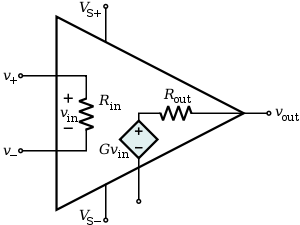
The circuit symbol for an op-amp is shown to the right, where:
The power supply pins (VS+ and VS−) can be labeled in different ways (See IC power supply pins). Despite different labeling, the function remains the same – to provide additional power for amplification of the signal. Often these pins are left out of the diagram for clarity, and the power configuration is described or assumed from the circuit.

where V+ is the voltage at the non-inverting terminal, V− is the voltage at the inverting terminal and AOL is the open-loop gain of the amplifier (the term "open-loop" refers to the absence of a feedback loop from the output to the input).
The magnitude of AOL is typically very large—10,000 or more for integrated circuit op-amps—and therefore even a quite small difference between V+ and V− drives the amplifier output nearly to the supply voltage. This is called saturation of the amplifier. The magnitude of AOL is not well controlled by the manufacturing process, and so it is impractical to use an operational amplifier as a stand-alone differential amplifier
. Without negative feedback, and perhaps with positive feedback
for regeneration
, an op-amp acts as a comparator
. If the inverting input is held at ground (0 V) directly or by a resistor, and the input voltage Vin applied to the non-inverting input is positive, the output will be maximum positive; if Vin is negative, the output will be maximum negative. Since there is no feedback from the output to either input, this is an open loop circuit acting as a comparator
. The circuit's gain is just the AOL< of the op-amp.
If predictable operation is desired, negative feedback is used, by applying a portion of the output voltage to the inverting input. The closed loop feedback greatly reduces the gain of the amplifier. If negative feedback is used, the circuit's overall gain and other parameters become determined more by the feedback network than by the op-amp itself. If the feedback network is made of components with relatively constant, stable values, the unpredictability and inconstancy of the op-amp's parameters do not seriously affect the circuit's performance. Typically the op-amp's very large gain is controlled by negative feedback, which largely determines the magnitude of its output ("closed-loop") voltage gain in amplifier applications, or the transfer function
required (in analog computers). High input impedance
at the input terminals and low output impedance at the output terminal(s) are important typical characteristics.
For example, in a non-inverting amplifier (see the figure on the right) adding a negative feedback via the voltage divider Rf,Rg reduces the gain. Equilibrium will be established when Vout is just sufficient to reach around and "pull" the inverting input to the same voltage as Vin. The voltage gain of the entire circuit is determined by 1 + Rf/Rg. As a simple example, if Vin = 1 V and Rf = Rg, Vout will be 2 V, the amount required to keep V– at 1 V. Because of the feedback provided by Rf,Rg this is a closed loop circuit. Its overall gain Vout / Vin is called the closed-loop gain ACL. Because the feedback is negative, in this case ACL is less than the AOL of the op-amp.
An ideal op-amp is usually considered to have the following properties, and they are considered to hold for all input voltages:
These ideals can be summarized by the two "golden rules":
The first rule only applies in the usual case where the op-amp is used in a closed-loop design (negative feedback, where there is a signal path of some sort feeding back from the output to the inverting input). These rules are commonly used as a good first approximation for analyzing or designing op-amp circuits.
In practice, none of these ideals can be perfectly realized, and various shortcomings and compromises have to be accepted. Depending on the parameters of interest, a real op-amp may be modeled to take account of some of the non-infinite or non-zero parameters using equivalent resistors and capacitors in the op-amp model. The designer can then include the effects of these undesirable, but real, effects into the overall performance of the final circuit. Some parameters may turn out to have negligible
effect on the final design while others represent actual limitations of the final performance, that must be evaluated.
Finite gain
Finite input impedance
s
Non-zero output impedance
Input current
Input offset voltage
Common-mode gain
Output sink current
Temperature effects
Power-supply rejection
Drift
Noise
Finite bandwidth
Input capacitance
Common-mode gain
Slewing
Non-linear
input-output relationship
Limited dissipated power
Modern integrated FET or MOSFET
op-amps approximate more closely the ideal op-amp than bipolar ICs when it comes to input impedance and input bias and offset currents. Bipolars are generally better when it comes to input voltage offset, and often have lower noise. Generally, at room temperature, with a fairly large signal, and limited bandwidth, FET and MOSFET op-amps now offer better performance.
Though designs vary between products and manufacturers, all op-amps have basically the same internal structure, which consists of three stages:
IC op-amps as implemented in practice are moderately complex integrated circuit
s. A typical example is the ubiquitous 741 op-amp designed by Dave Fullagar in Fairchild Semiconductor
after the remarkable Widlar LM301. Thus the basic architecture of the 741 is identical to that of the 301.
with a complex biasing circuit and a current mirror active load
.
pair Q3 and Q4 that eliminates the undesired Miller effect
, shifts the voltage level downwards and provides a sufficient voltage gain to drive the next class A amplifier. The PNP transistors also help to increase the reverse Vbe rating (the base-emitter junctions of the NPN transistors Q1 and Q2 break down at around 7 V but the PNP transistors Q3 and Q4 have breakdown voltages around 50 V).
Here, the Q3/Q4 emitters are already used as inputs. Their collectors are separated and cannot be used as inputs for the quiescent current source since they behave as current sources. So, the quiescent current can be set only from the side of the bases by connecting a constant current source to them. To make it not depend on β as above, a negative but parallel feedback is used. For this purpose, the total quiescent current is mirrored by Q8-Q9 current mirror and the negative feedback is taken from the Q9 collector. Now it makes the transistors Q1-Q4 adjust their VBE voltages so that to pass the desired quiescent current. The effect is the same as at the classical emitter-coupled pair - the quiescent current is β-independent. It is interesting fact that "to the extent that all PNP βs match, this clever circuit generates just the right β-dependent base current to produce a β-independent collector current". The biasing base currents are usually provided only by the negative power supply; they should come from the ground and enter the bases. But to ensure maximum high input impedances, the biasing loops are not internally closed between the base and ground; it is expected they will be closed externally by the input sources. So, the sources have to be galvanic (DC) to ensure paths for the biasing currents and low resistive enough (tens or hundreds kilohms) to not create significant voltage drops across them. Otherwise, additional DC elements should be connected between the bases and the ground (or the positive power supply).
The quiescent current is set by the 39 kΩ resistor that is common for the two current mirrors Q12-Q13 and Q10-Q11. The current determined by this resistor acts also as a reference for the other bias currents used in the chip. The Widlar current mirror built by Q10, Q11, and the 5 kΩ resistor produces a very small fraction of at the Q10 collector. This small constant current through Q10's collector supplies the base currents for Q3 and Q4 as well as the Q9 collector current. The Q8/Q9 current mirror tries to make Q9 collector current the same as the Q3 and Q4 collector currents and succeeds with the help of the negative feedback. The Q9 collector voltage changes until the ratio between the Q3/Q4 base and collector currents becomes equal to β. Thus Q3 and Q4's combined base currents (which are of the same order as the overall chip's input currents) are a small fraction of the already small Q10 current.
Thus the quiescent current is set by Q10-Q11 current mirror without using a current-sensing negative feedback. The voltage-sensing negative feedback only helps this process by stabilizing Q9 collector (Q3/Q4 base) voltage.This arrangement can be generalized by an equivalent circuit consisting of a constant current source loaded by a voltage source; the voltage source fixes the voltage across the current source while the current source sets the current through the voltage source. As the two heterogeneous sources provide ideal load conditions for each other, this circuit solution is widely used in cascode circuits
, Wilson current mirror, the input part of the simple current mirror
, emitter-coupled and other exotic circuits. The feedback loop also isolates the rest of the circuit from common-mode signal
s by making the base voltage of Q3/Q4 follow tightly below the higher of the two input voltages.
implemented as an improved current mirror (Q5–Q7) whose role is to convert the differential current input signal to a single ended voltage signal without the intrinsic 50% losses and to increase extremely the gain. This is achieved by copying the input signal from the left to the right side where the magnitudes of the two input signals add (Widlar used the same trick in μA702 and μA709). For this purpose, the input of the current mirror (Q5 collector) is connected to the left output (Q3 collector) and the output of the current mirror (Q6 collector) is connected to the right output of the differential amplifier (Q4 collector). Q7 increases the accuracy of the current mirror by decreasing the amount of signal current required from Q3 to drive the bases of Q5 and Q6.
The input voltage sources are connected through two "diode" strings, each of them consisting of two connected in series base-emitter junctions (Q1-Q3 and Q2-Q4), to the common point of Q3/Q4 bases. So, if the input voltages change slightly in opposite directions, Q3/Q4 bases stay at relatively constant voltage and the common base current does not change as well; it only vigorously steers between Q3/Q4 bases and makes the common quiescent current distribute between Q3/Q4 collectors in the same proportion.If the input differential voltage changes significantly (with more than about a hundred millivolts), the base-emitter junctions of the transistors driven by the lower input voltage (e.g., Q1 and Q3) become backward biased and the total common base current flows through the other (Q2 and Q4) base-emitter junctions. However, the high breakdown voltage of the PNP transistors Q3/Q4 prevents Q1/Q2 base-emitter junctions from damaging when the input difference voltage increases up to 50 V because of the unlimited current that may flow directly through the "diode bridge" between the two input sources. The current mirror inverts Q3 collector current and tries to pass it through Q4. In the middle point between Q4 and Q6, the signal currents (current changes) of Q3 and Q4 are subtracted. In this case (differential input signal), they are equal and opposite. Thus, the difference is twice the individual signal currents (ΔI - (-ΔI) = 2ΔI) and the differential to single ended conversion is completed without gain losses. The open circuit signal voltage appearing at this point is given by the product of the subtracted signal currents and the total circuit impedance (the paralleled collector resistances of Q4 and Q6). Since the collectors of Q4 and Q6 appear as high differential resistances to the signal current (Q4 and Q6 behave as current sources), the open circuit voltage gain of this stage is very high.This circuit (and geometrical) phenomenon can be illustrated graphically by superimposing the Q4 and Q6 output characteristics (almost parallel horizontal lines) on the same coordinate system. When the input voltages vary slightly in opposite directions, the two curves move slightly toward each other in the vertical direction but the operating (cross) point moves vigorously in the horizontal direction. The ratio between the two movements represents the high amplification.
More intuitively, the transistor Q6 can be considered as a duplicate of Q3 and the combination of Q4 and Q6 can be thought as of a varying voltage divider composed of two voltage-controlled resistors. For differential input signals, they vigorously change their instant resistances in opposite directions but the total resistance stays constant (like a potentiometer with quickly moving slider). As a result, the current stays constant as well but the voltage at the middle point changes vigorously. As the two resistance changes are equal and opposite, the effective voltage change is twice the individual change.
The base current at the inputs is not zero and the effective differential input impedance of a 741 is about 2 MΩ. The "offset null" pins may be used to place external resistors in parallel with the two 1 kΩ resistors (typically in the form of the two ends of a potentiometer) to adjust the balancing of the Q5/Q6 current mirror and thus indirectly control the output of the op-amp when zero signal is applied between the inputs.
If the input voltages change in the same direction, the negative feedback makes Q3/Q4 base voltage follow (with 2VBE below) the input voltage variations. Now the output part (Q10) of Q10-Q11 current mirror keeps up the common current through Q9/Q8 constant in spite of varying voltage. Q3/Q4 collector currents and accordingly, the output voltage in the middle point between Q4 and Q6, remain unchanged.
The following negative feedback (bootstrapping) increases virtually the effective op-amp common-mode input impedance.
is the class A gain stage. The top-right current mirror Q12/Q13 supplies this stage by a constant current load, via the collector of Q13, that is largely independent of the output voltage. The stage consists of the two NPN transistors Q15/Q19 connected in a Darlington configuration
and uses the output side of a current mirror as its collector (dynamic) load to achieve high gain
. The transistor Q22 prevents this stage from saturating by diverting the excessive Q15 base current (it acts as a Baker clamp
).
The 30 pF capacitor provides frequency selective negative feedback around the class A gain stage as a means of frequency compensation
to stabilise the amplifier in feedback configurations. This technique is called Miller compensation
and functions in a similar manner to an op-amp integrator
circuit. It is also known as 'dominant pole compensation' because it introduces a dominant pole (one which masks the effects of other poles) into the open loop
frequency response. This pole can be as low as 10 Hz in a 741 amplifier and it introduces a −3 dB loss into the open loop response at this frequency. This internal compensation is provided to achieve unconditional stability
of the amplifier in negative feedback configurations where the feedback network is non-reactive and the closed loop gain is unity or higher. Hence, the use of the operational amplifier is simplified because no external compensation is required for unity gain stability; amplifiers without this internal compensation such as the 748 may require external compensation or closed-loop gains significantly higher than unity.
(in some discrete component amplifiers, this function is usually achieved with a string of two silicon diodes).
The circuit can be presented as a negative feedback voltage amplifier with constant input voltage of 0.625 V and a feedback ratio of β = 0.625 (a gain of 1/β = 1.6). The same circuit but with β = 1 is used in the input current-setting part of the classical BJT current mirror.
) is a Class AB push-pull emitter follower (Q14, Q20) amplifier with the bias set by the multiplier voltage source Q16 and its base resistors. This stage is effectively driven by the collectors of Q13 and Q19. Variations in the bias with temperature, or between parts with the same type number, are common so crossover distortion
and quiescent current may be subject to significant variation. The output range of the amplifier is about one volt less than the supply voltage, owing in part to of the output transistors Q14 and Q20.
The 25 Ω resistor in the output stage acts as a current sense to provide the output current-limiting function which limits the current in the emitter follower Q14 to about 25 mA for the 741. Current limiting for the negative output is done by sensing the voltage across Q19's emitter resistor and using this to reduce the drive into Q15's base. Later versions of this amplifier schematic may show a slightly different method of output current limiting.
The output resistance is not zero, as it would be in an ideal op-amp, but with negative feedback it approaches zero at low frequencies.
performance of more modern op-amps. Apart from generating noticeable hiss, 741s and other older op-amps may have poor common-mode rejection ratio
s and so will often introduce cable-borne mains hum and other common-mode interference, such as switch 'clicks', into sensitive equipment.
The "741" has come to often mean a generic op-amp IC (such as μA741, LM301, 558, LM324, TBA221 - or a more modern replacement such as the TL071). The description of the 741 output stage is qualitatively similar for many other designs (that may have quite different input stages), except:
IC op-amps may be classified in many ways, including:

Circuit design follows the same lines for all electronic circuits. A specification is drawn up governing what the circuit is required to do, with allowable limits. For example, the gain may be required to be 100 times, with a tolerance of 5% but drift of less than 1% in a specified temperature range; the input impedance not less than one megohm; etc.
A basic circuit
is designed, often with the help of circuit modeling (on a computer). Specific commercially available op-amps and other components are then chosen that meet the design criteria within the specified tolerances at acceptable cost. If not all criteria can be met, the specification may need to be modified.
A prototype is then built and tested; changes to meet or improve the specification, alter functionality, or reduce the cost, may be made.
A voltage level detector can be obtained if a reference voltage Vref is applied to one of the op-amp's inputs. This means that the op-amp is set up as a comparator to detect a positive voltage. If the voltage to be sensed, Ei, is applied to op amp's (+) input, the result is a noninverting positive-level detector: when Ei is above Vref, VO equals +Vsat; when Ei is below Vref, VO equals -Vsat. If Ei is applied to the inverting input, the circuit is an inverting positive-level detector: When Ei is above Vref, VO equals -Vsat.
A zero voltage level detector (Ei = 0) can convert, for example, the output of a sine-wave from a function generator into a variable-frequency square wave. If Ei is a sine wave, triangular wave, or wave of any other shape that is symmetrical around zero, the zero-crossing detector's output will be square. Zero-crossing detection may also be useful in triggering TRIAC
s at the best time to reduce mains interference and current spikes.
oscillators and active filters.
Because of the wide slew-range and lack of positive feedback, the response of all the open-loop level detectors described above will be relatively slow. External overall positive feedback may be applied but (unlike internal positive feedback that may be applied within the latter stages of a purpose-designed comparator) this markedly affects the accuracy of the zero-crossing detection point. Using a general-purpose op-amp, for example, the frequency of Ei for the sine to square wave converter should probably be below 100 Hz.
 In a non-inverting amplifier, the output voltage changes in the same direction as the input voltage.
The gain equation for the op-amp is:

However, in this circuit – is a function of
  because of the negative feedback through the
  network.
  and
and  form a voltage divider, and as
  – is a high-impedance input, it does not load it appreciably. Consequently:

where

Substituting this into the gain equation, we obtain:

Solving for :
:

If is very large, this simplifies to
 .
.
Note that the non-inverting input of the operational amplifier will need a path for DC to ground; if the signal source might not give this, or if that source requires a given load impedance, the circuit will require another resistor - from input to ground. In either case, the ideal value for the feedback resistors (to give minimum offset voltage) will be such that the two resistances in parallel roughly equal the resistance to ground at the non-inverting input pin.
 In an inverting amplifier, the output voltage changes in an opposite direction to the input voltage.
As with the non-inverting amplifier, we start with the gain equation of the op-amp:

This time, – is a function of both
  and
and  due to the voltage divider formed by
  and
and  . Again, the op-amp input does not apply an appreciable load, so:

Substituting this into the gain equation and solving for :
:

If is very large, this simplifies to
 .
.
A resistor is often inserted between the non-inverting input and ground (so both inputs "see" similar resistances), reducing the input offset voltage
due to different voltage drops due to bias current, and may reduce distortion in some op-amps.
A DC-blocking
capacitor
may be inserted in series with the input resistor when a frequency response
down to DC is not needed and any DC voltage on the input is unwanted. That is, the capacitive component of the input impedance inserts a DC zero and a low-frequency pole that gives the circuit a bandpass or high-pass characteristic.
The potentials at the operational amplifier inputs remain virtually constant (near ground) in the inverting configuration. The constant operating potential typically results in distortion levels that are lower than those attainable with the non-inverting topology.
Most single, dual and quad op-amps available have a standardized pin-out which permits one type to be substituted for another without wiring changes. A specific op-amp may be chosen for its open loop gain, bandwidth, noise performance, input impedance, power consumption, or a compromise between any of these factors.
, is first found in "Summing Amplifier" filed by Karl D. Swartzel Jr. of Bell Labs in 1941. This design used three vacuum tube
s to achieve a gain of and operated on voltage rails of . It had a single inverting input rather than differential inverting and non-inverting inputs, as are common in today's op-amps. Throughout World War II
, Swartzel's design proved its value by being liberally used in the M9 artillery director
designed at Bell Labs. This artillery director worked with the SCR584 radar
system to achieve extraordinary hit rates (near 90%) that would not have been possible otherwise.
 1947: An op-amp with an explicit non-inverting input. In 1947, the operational amplifier was first formally defined and named in a paper by Professor John R. Ragazzini of Columbia University. In this same paper a footnote mentioned an op-amp design by a student that would turn out to be quite significant. This op-amp, designed by Loebe Julie, was superior in a variety of ways. It had two major innovations. Its input stage used a long-tailed triode
pair with loads matched to reduce drift
in the output and, far more importantly, it was the first op-amp design to have two inputs (one inverting, the other non-inverting). The differential input made a whole range of new functionality possible, but it would not be used for a long time due to the rise of the chopper-stabilized amplifier.
1949: A chopper-stabilized op-amp. In 1949, Edwin A. Goldberg designed a chopper
-stabilized op-amp. This set-up uses a normal op-amp with an additional AC
amplifier that goes alongside the op-amp. The chopper gets an AC signal from DC
by switching between the DC voltage and ground at a fast rate (60 Hz or 400 Hz). This signal is then amplified, rectified, filtered and fed into the op-amp's non-inverting input. This vastly improved the gain of the op-amp while significantly reducing the output drift and DC offset. Unfortunately, any design that used a chopper couldn't use their non-inverting input for any other purpose. Nevertheless, the much improved characteristics of the chopper-stabilized op-amp made it the dominant way to use op-amps. Techniques that used the non-inverting input regularly would not be very popular until the 1960s when op-amp IC
s started to show up in the field.
In 1953, vacuum tube op-amps became commercially available with the release of the model K2-W from George A. Philbrick Researches, Incorporated. The designation on the devices shown, GAP/R, is an acronym for the complete company name. Two nine-pin 12AX7 vacuum tubes were mounted in an octal package and had a model K2-P chopper add-on available that would effectively "use up" the non-inverting input. This op-amp was based on a descendant of Loebe Julie's 1947 design and, along with its successors, would start the widespread use of op-amps in industry.
 1961: A discrete IC op-amps. With the birth of the transistor
in 1947, and the silicon transistor in 1954, the concept of ICs became a reality. The introduction of the planar process
in 1959 made transistors and ICs stable enough to be commercially useful. By 1961, solid-state, discrete op-amps were being produced. These op-amps were effectively small circuit boards with packages such as edge connector
s. They usually had hand-selected resistors in order to improve things such as voltage offset and drift. The P45 (1961) had a gain of 94 dB and ran on ±15 V rails. It was intended to deal with signals in the range of .
1961: A varactor bridge op-amps. There have been many different directions taken in op-amp design. Varactor bridge op-amps started to be produced in the early 1960s. They were designed to have extremely small input current and are still amongst the best op-amps available in terms of common-mode rejection with the ability to correctly deal with hundreds of volts at their inputs.
 1962: An op-amps in potted modules. By 1962, several companies were producing modular potted packages that could be plugged into printed circuit board
s. These packages were crucially important as they made the operational amplifier into a single black box
which could be easily treated as a component in a larger circuit.
1963: A monolithic IC op-amp. In 1963, the first monolithic IC op-amp, the μA702 designed by Bob Widlar
at Fairchild Semiconductor, was released. Monolithic IC
s consist of a single chip as opposed to a chip and discrete parts (a discrete IC) or multiple chips bonded and connected on a circuit board (a hybrid IC). Almost all modern op-amps are monolithic ICs; however, this first IC did not meet with much success. Issues such as an uneven supply voltage, low gain and a small dynamic range held off the dominance of monolithic op-amps until 1965 when the μA709 (also designed by Bob Widlar) was released.
1968: Release of the μA741. The popularity of monolithic op-amps was further improved upon the release of the LM101 in 1967, which solved a variety of issues, and the subsequent release of the μA741 in 1968. The μA741 was extremely similar to the LM101 except that Fairchild's facilities allowed them to include a 30 pF compensation capacitor inside the chip instead of requiring external compensation. This simple difference has made the 741 the canonical op-amp and many modern amps base their pinout on the 741s. The μA741 is still in production, and has become ubiquitous in electronics—many manufacturers produce a version of this classic chip, recognizable by part numbers containing 741. The same part is manufactured by several companies.
1970: First high-speed, low-input current FET design.
In the 1970s high speed, low-input current designs started to be made by using FET
s. These would be largely replaced by op-amps made with MOSFET
s in the 1980s. During the 1970s single sided supply op-amps also became available.
 1972: Single sided supply op-amps being produced. A single sided supply op-amp is one where the input and output voltages can be as low as the negative power supply voltage instead of needing to be at least two volts above it. The result is that it can operate in many applications with the negative supply pin on the op-amp being connected to the signal ground, thus eliminating the need for a separate negative power supply.
The LM324 (released in 1972) was one such op-amp that came in a quad package (four separate op-amps in one package) and became an industry standard. In addition to packaging multiple op-amps in a single package, the 1970s also saw the birth of op-amps in hybrid packages. These op-amps were generally improved versions of existing monolithic op-amps. As the properties of monolithic op-amps improved, the more complex hybrid ICs were quickly relegated to systems that are required to have extremely long service lives or other specialty systems.
 Recent trends. Recently supply voltages in analog circuits have decreased (as they have in digital logic) and low-voltage op-amps have been introduced reflecting this. Supplies of ±5 V and increasingly 3.3 V (sometimes as low as 1.8 V) are common. To maximize the signal range modern op-amps commonly have rail-to-rail output (the output signal can range from the lowest supply voltage to the highest) and sometimes rail-to-rail inputs.
Direct current
Direct current is the unidirectional flow of electric charge. Direct current is produced by such sources as batteries, thermocouples, solar cells, and commutator-type electric machines of the dynamo type. Direct current may flow in a conductor such as a wire, but can also flow through...
-coupled
Direct coupling
In electronics, direct coupling is a way of interconnecting two circuits such that, in addition to transferring the AC signal , the first stage also provides DC bias to the next...
high-gain
Gain
In electronics, gain is a measure of the ability of a circuit to increase the power or amplitude of a signal from the input to the output. It is usually defined as the mean ratio of the signal output of a system to the signal input of the same system. It may also be defined on a logarithmic scale,...
electronic voltage amplifier
Electronic amplifier
An electronic amplifier is a device for increasing the power of a signal.It does this by taking energy from a power supply and controlling the output to match the input signal shape but with a larger amplitude...
with a differential input and, usually, a single-ended output. An op-amp produces an output voltage that is typically hundreds of thousands times larger than the voltage difference between its input terminals.
Operational amplifiers are important building blocks for a wide range of electronic circuits. They had their origins in analog computers where they were used in many linear, non-linear and frequency-dependent circuits. Their popularity in circuit design largely stems from the fact that characteristics of the final op-amp circuits with negative feedback
Negative feedback
Negative feedback occurs when the output of a system acts to oppose changes to the input of the system, with the result that the changes are attenuated. If the overall feedback of the system is negative, then the system will tend to be stable.- Overview :...
(such as their gain
Gain
In electronics, gain is a measure of the ability of a circuit to increase the power or amplitude of a signal from the input to the output. It is usually defined as the mean ratio of the signal output of a system to the signal input of the same system. It may also be defined on a logarithmic scale,...
) are set by external components with little dependence on temperature changes and manufacturing variations in the op-amp itself.
Op-amps are among the most widely used electronic devices today, being used in a vast array of consumer, industrial, and scientific devices. Many standard IC op-amps cost only a few cents in moderate production volume; however some integrated or hybrid operational amplifiers with special performance specifications may cost over $100 US in small quantities. Op-amps may be packaged as components, or used as elements of more complex integrated circuits.
The op-amp is one type of differential amplifier
Differential amplifier
A differential amplifier is a type of electronic amplifier that amplifies the difference between two voltages but does not amplify the particular voltages.- Theory :Many electronic devices use differential amplifiers internally....
. Other types of differential amplifier include the fully differential amplifier
Fully differential amplifier
A fully differential amplifier, usually referred to as an FDA for brevity, is a DC-coupled high-gain electronic voltage amplifier with differential inputs and differential outputs...
(similar to the op-amp, but with two outputs), the instrumentation amplifier
Instrumentation amplifier
An instrumentation amplifier is a type of differential amplifier that has been outfitted with input buffers, which eliminate the need for input impedance matching and thus make the amplifier particularly suitable for use in measurement and test equipment...
(usually built from three op-amps), the isolation amplifier
Isolation amplifier
Isolation amplifiers provide electrical isolation and an electrical safety barrier. They protect data acquisition components from common mode voltages, which are potential differences between instrument ground and signal ground...
(similar to the instrumentation amplifier, but with tolerance to common-mode voltages that would destroy an ordinary op-amp), and negative feedback amplifier (usually built from one or more op-amps and a resistive feedback network).
Circuit notation
- V+: non-inverting input
- V−: inverting input
- Vout: output
- VS+: positive power supply
- VS−: negative power supply
The power supply pins (VS+ and VS−) can be labeled in different ways (See IC power supply pins). Despite different labeling, the function remains the same – to provide additional power for amplification of the signal. Often these pins are left out of the diagram for clarity, and the power configuration is described or assumed from the circuit.
Operation
The amplifier's differential inputs consist of a V+ input and a V− input, and ideally the op-amp amplifies only the difference in voltage between the two, which is called the differential input voltage. The output voltage of the op-amp is given by the equation,where V+ is the voltage at the non-inverting terminal, V− is the voltage at the inverting terminal and AOL is the open-loop gain of the amplifier (the term "open-loop" refers to the absence of a feedback loop from the output to the input).
The magnitude of AOL is typically very large—10,000 or more for integrated circuit op-amps—and therefore even a quite small difference between V+ and V− drives the amplifier output nearly to the supply voltage. This is called saturation of the amplifier. The magnitude of AOL is not well controlled by the manufacturing process, and so it is impractical to use an operational amplifier as a stand-alone differential amplifier
Differential amplifier
A differential amplifier is a type of electronic amplifier that amplifies the difference between two voltages but does not amplify the particular voltages.- Theory :Many electronic devices use differential amplifiers internally....
. Without negative feedback, and perhaps with positive feedback
Positive feedback
Positive feedback is a process in which the effects of a small disturbance on a system include an increase in the magnitude of the perturbation. That is, A produces more of B which in turn produces more of A. In contrast, a system that responds to a perturbation in a way that reduces its effect is...
for regeneration
Regenerative circuit
The regenerative circuit or "autodyne" allows an electronic signal to be amplified many times by the same vacuum tube or other active component such as a field effect transistor. It consists of an amplifying vacuum tube or transistor with its output connected to its input through a feedback...
, an op-amp acts as a comparator
Comparator
In electronics, a comparator is a device that compares two voltages or currents and switches its output to indicate which is larger. They are commonly used in devices such as Analog-to-digital converters .- Input voltage range :...
. If the inverting input is held at ground (0 V) directly or by a resistor, and the input voltage Vin applied to the non-inverting input is positive, the output will be maximum positive; if Vin is negative, the output will be maximum negative. Since there is no feedback from the output to either input, this is an open loop circuit acting as a comparator
Comparator
In electronics, a comparator is a device that compares two voltages or currents and switches its output to indicate which is larger. They are commonly used in devices such as Analog-to-digital converters .- Input voltage range :...
. The circuit's gain is just the AOL< of the op-amp.
If predictable operation is desired, negative feedback is used, by applying a portion of the output voltage to the inverting input. The closed loop feedback greatly reduces the gain of the amplifier. If negative feedback is used, the circuit's overall gain and other parameters become determined more by the feedback network than by the op-amp itself. If the feedback network is made of components with relatively constant, stable values, the unpredictability and inconstancy of the op-amp's parameters do not seriously affect the circuit's performance. Typically the op-amp's very large gain is controlled by negative feedback, which largely determines the magnitude of its output ("closed-loop") voltage gain in amplifier applications, or the transfer function
Transfer function
A transfer function is a mathematical representation, in terms of spatial or temporal frequency, of the relation between the input and output of a linear time-invariant system. With optical imaging devices, for example, it is the Fourier transform of the point spread function i.e...
required (in analog computers). High input impedance
Electrical impedance
Electrical impedance, or simply impedance, is the measure of the opposition that an electrical circuit presents to the passage of a current when a voltage is applied. In quantitative terms, it is the complex ratio of the voltage to the current in an alternating current circuit...
at the input terminals and low output impedance at the output terminal(s) are important typical characteristics.
For example, in a non-inverting amplifier (see the figure on the right) adding a negative feedback via the voltage divider Rf,Rg reduces the gain. Equilibrium will be established when Vout is just sufficient to reach around and "pull" the inverting input to the same voltage as Vin. The voltage gain of the entire circuit is determined by 1 + Rf/Rg. As a simple example, if Vin = 1 V and Rf = Rg, Vout will be 2 V, the amount required to keep V– at 1 V. Because of the feedback provided by Rf,Rg this is a closed loop circuit. Its overall gain Vout / Vin is called the closed-loop gain ACL. Because the feedback is negative, in this case ACL is less than the AOL of the op-amp.
Ideal op-amps
- Infinite open-loop gainOpen-loop gainThe open-loop gain of an operational amplifier is the gain obtained when no feedback is used in the circuit.Open loop gain is usually exceedingly high; in fact, an ideal operational amplifier has infinite open-loop gain. Typically an op-amp may have an open-loop gain of around 10^5...
(when doing theoretical analysis, a limitLimit of a functionIn mathematics, the limit of a function is a fundamental concept in calculus and analysis concerning the behavior of that function near a particular input....
may be taken as open loop gain AOL goes to infinity). - Infinite voltage range available at the output (
 ) (in practice the voltages available from the output are limited by the supply voltages
  and
and  ). The power supply sources are called rails.
 - Infinite bandwidth (i.e., the frequency magnitude response is considered to be flat everywhere with zero phase shift).
- Infinite input impedanceInput impedanceThe input impedance of an electrical network is the equivalent impedance "seen" by a power source connected to that network. If the source provides known voltage and current, such impedance can be calculated using Ohm's Law...
(so, in the diagram, , and zero current flows from
  to
to  ).
). - Zero input current (i.e., there is assumed to be no leakage or biasBiasing (electronics)Biasing in electronics is the method of establishing predetermined voltages and/or currents at various points of an electronic circuit to set an appropriate operating point...
current into the device). - Zero input offset voltageInput offset voltageInput offset voltage is the differential DC voltage required between the inputs of an amplifier, especially an operational amplifier, to make the output zero .* Typical values are around 1-10mV for cheap commercial-grade operational amplifier integrated circuits, but can...
(i.e., when the input terminals are shorted so that , the output is a virtual groundVirtual groundVirtual ground is a node of the circuit that is maintained at a steady reference potential, without being connected directly to the reference potential...
or ).
). - Infinite slew rateSlew rateIn electronics, the slew rate represents the maximum rate of change of a signal at any point in a circuit.Limitations in slew rate capability can give rise to non linear effects in electronic amplifiers...
(i.e., the rate of change of the output voltage is unbounded) and power bandwidth (full output voltage and current available at all frequencies). - Zero output impedanceOutput impedanceThe output impedance, source impedance, or internal impedance of an electronic device is the opposition exhibited by its output terminals to an alternating current of a particular frequency as a result of resistance, inductance and capacitance...
(i.e., , so that output voltage does not vary with output current).
 - Zero noiseElectronic noiseElectronic noise is a random fluctuation in an electrical signal, a characteristic of all electronic circuits. Noise generated by electronic devices varies greatly, as it can be produced by several different effects...
. - Infinite Common-mode rejection ratioCommon-mode rejection ratioThe common-mode rejection ratio of a differential amplifier is the tendency of the devices to reject the input signals common to both input leads...
(CMRR). - Infinite Power supply rejection ratioPower supply rejection ratioIn electronics, power supply rejection ratio or PSRR is a term widely used in the electronic amplifier or voltage regulator datasheets; used to describe the amount of noise from a power supply that a particular device can reject.-Definition:The PSRR is defined as the ratio of the change in supply...
for both power supply rails.
These ideals can be summarized by the two "golden rules":
- I. The output attempts to do whatever is necessary to make the voltage difference between the inputs zero.
- II. The inputs draw no current.
The first rule only applies in the usual case where the op-amp is used in a closed-loop design (negative feedback, where there is a signal path of some sort feeding back from the output to the inverting input). These rules are commonly used as a good first approximation for analyzing or designing op-amp circuits.
In practice, none of these ideals can be perfectly realized, and various shortcomings and compromises have to be accepted. Depending on the parameters of interest, a real op-amp may be modeled to take account of some of the non-infinite or non-zero parameters using equivalent resistors and capacitors in the op-amp model. The designer can then include the effects of these undesirable, but real, effects into the overall performance of the final circuit. Some parameters may turn out to have negligible
Negligible
Negligible refers to the quantities so small that they can be ignored when studying the larger effect. Although related to the more mathematical concepts of infinitesimal, the idea of negligibility is particularly useful in practical disciplines like physics, chemistry, mechanical and electronic...
effect on the final design while others represent actual limitations of the final performance, that must be evaluated.
DC imperfections
Real operational amplifiers suffer from several non-ideal effects:Finite gain
Gain
In electronics, gain is a measure of the ability of a circuit to increase the power or amplitude of a signal from the input to the output. It is usually defined as the mean ratio of the signal output of a system to the signal input of the same system. It may also be defined on a logarithmic scale,...
- Open-loop gainOpen-loop gainThe open-loop gain of an operational amplifier is the gain obtained when no feedback is used in the circuit.Open loop gain is usually exceedingly high; in fact, an ideal operational amplifier has infinite open-loop gain. Typically an op-amp may have an open-loop gain of around 10^5...
is infinite in the ideal operational amplifier but finite in real operational amplifiers. Typical devices exhibit open-loop DC gain ranging from 100,000 to over 1 million. So long as the loop gainLoop gainLoop gain is an engineering term used to quantify the gain of a system controlled by feedback loops. As such, the concept of loop gain is useful in a variety of disciplines. Traditionally, most of those have been in the field of electronics, telecommunications, or control systems...
(i.e., the product of open-loop and feedback gains) is very large, the circuit gain will be determined entirely by the amount of negative feedback (i.e., it will be independent of open-loop gain). In cases where closed-loop gain must be very high, the feedback gain will be very low, and the low feedback gain causes low loop gain; in these cases, the operational amplifier will cease to behave ideally.
Finite input impedance
Input impedance
The input impedance of an electrical network is the equivalent impedance "seen" by a power source connected to that network. If the source provides known voltage and current, such impedance can be calculated using Ohm's Law...
s
- The differential input impedance of the operational amplifier is defined as the impedance between its two inputs; the common-mode input impedance is the impedance from each input to ground. MOSFETMOSFETThe metal–oxide–semiconductor field-effect transistor is a transistor used for amplifying or switching electronic signals. The basic principle of this kind of transistor was first patented by Julius Edgar Lilienfeld in 1925...
-input operational amplifiers often have protection circuits that effectively short circuit any input differences greater than a small threshold, so the input impedance can appear to be very low in some tests. However, as long as these operational amplifiers are used in a typical high-gain negative feedback application, these protection circuits will be inactive. The input bias and leakage currents described below are a more important design parameter for typical operational amplifier applications.
Non-zero output impedance
Output impedance
The output impedance, source impedance, or internal impedance of an electronic device is the opposition exhibited by its output terminals to an alternating current of a particular frequency as a result of resistance, inductance and capacitance...
- Low output impedance is important for low-impedance loads; for these loads, the voltage drop across the output impedance of the amplifier will be significant. Hence, the output impedance of the amplifier limits the maximum power that can be provided. In configurations with a voltage-sensing negative feedback, the output impedance of the amplifier is effectively lowered; thus, in linear applications, op-amps usually exhibit a very low output impedance indeed. Negative feedback can not, however, reduce the limitations that Rload in conjunction with Rout place on the maximum and minimum possible output voltages; it can only reduce output errors within that range.
- Low-impedance outputs typically require high quiescent (i.e., idle) current in the output stage and will dissipate more power, so low-power designs may purposely sacrifice low output impedance.
Input current
- Due to biasingBiasing (electronics)Biasing in electronics is the method of establishing predetermined voltages and/or currents at various points of an electronic circuit to set an appropriate operating point...
requirements or leakage, a small amount of current (typically ~10 nanoamperes for bipolarBipolar-Medicine:* Bipolar cell* Bipolar cell of the retina* Bipolar disorder** Bipolar I disorder** Bipolar II disorder** Bipolar NOS* Bipolar spectrum-Astronomy:* Bipolar nebula, a two-lobed, axially symmetric nebula...
op-amps, tens of picoamperes for JFETJFETThe junction gate field-effect transistor is the simplest type of field-effect transistor. It can be used as an electronically-controlled switch or as a voltage-controlled resistance. Electric charge flows through a semiconducting channel between "source" and "drain" terminals...
input stages, and only a few pA for MOSFETMOSFETThe metal–oxide–semiconductor field-effect transistor is a transistor used for amplifying or switching electronic signals. The basic principle of this kind of transistor was first patented by Julius Edgar Lilienfeld in 1925...
input stages) flows into the inputs. When large resistors or sources with high output impedances are used in the circuit, these small currents can produce large unmodeled voltage drops. If the input currents are matched, and the impedance looking out of both inputs are matched, then the voltages produced at each input will be equal. Because the operational amplifier operates on the difference between its inputs, these matched voltages will have no effect (unless the operational amplifier has poor CMRRCommon-mode rejection ratioThe common-mode rejection ratio of a differential amplifier is the tendency of the devices to reject the input signals common to both input leads...
, which is described below). It is more common for the input currents (or the impedances looking out of each input) to be slightly mismatched, and so a small offset voltage (different from the input offset voltage below) can be produced. This offset voltage can create offsets or drifting in the operational amplifier. It can often be nulled externally; however, many operational amplifiers include offset null or balance pins and some procedure for using them to remove this offset. Some operational amplifiers attempt to nullify this offset automatically.
Input offset voltage
- This voltage, which is what is required across the op-amp's input terminals to drive the output voltage to zero,This definition hews to the convention of measuring op-amp parameters with respect to the zero voltage point in the circuit, which is usually half the total voltage between the amplifier's positive and negative power rails. is related to the mismatches in input bias current. In the perfect amplifier, there would be no input offset voltage. However, it exists in actual op-amps because of imperfections in the differential amplifier that constitutes the input stage of the vast majority of these devices. Input offset voltage creates two problems: First, due to the amplifier's high voltage gain, it virtually assures that the amplifier output will go into saturation if it is operated without negative feedback, even when the input terminals are wired together. Second, in a closed loop, negative feedback configuration, the input offset voltage is amplified along with the signal and this may pose a problem if high precision DC amplification is required or if the input signal is very small.Many older designs of operational amplifiers have offset null inputs to allow the offset to be manually adjusted away. Modern precision op-amps can have internal circuits that automatically cancel this offset using chopperChopper (electronics)A chopper circuit is used to refer to numerous types of electronic switching devices and circuits. The term has become somewhat ill-defined, and as a result is much less used nowadays than it was perhaps 30 or more years ago....
s or other circuits that measure the offset voltage periodically and subtract it from the input voltage.
Common-mode gain
- A perfect operational amplifier amplifies only the voltage difference between its two inputs, completely rejecting all voltages that are common to both. However, the differential input stage of an operational amplifier is never perfect, leading to the amplification of these identical voltages to some degree. The standard measure of this defect is called the common-mode rejection ratioCommon-mode rejection ratioThe common-mode rejection ratio of a differential amplifier is the tendency of the devices to reject the input signals common to both input leads...
(denoted CMRR). Minimization of common mode gain is usually important in non-inverting amplifiers (described below) that operate at high amplification.
Output sink current
- The output sink current is maximum current allowed to sink into the output stage. Some manufacturers show the output voltage vs. the output sink current plot, which gives an idea of the output voltage when it is sinking current from another source into the output pin.
Temperature effects
- All parameters change with temperature. Temperature drift of the input offset voltage is especially important.
Power-supply rejection
- The output of a perfect operational amplifier will be completely independent from ripples that arrive on its power supply inputs. Every real operational amplifier has a specified power supply rejection ratioPower supply rejection ratioIn electronics, power supply rejection ratio or PSRR is a term widely used in the electronic amplifier or voltage regulator datasheets; used to describe the amount of noise from a power supply that a particular device can reject.-Definition:The PSRR is defined as the ratio of the change in supply...
(PSRR) that reflects how well the op-amp can reject changes in its supply voltage. Copious use of bypass capacitors can improve the PSRR of many devices, including the operational amplifier.
Drift
- Real op-amp parameters are subject to slow change over time and with changes in temperature, input conditions, etc.
Noise
- Amplifiers generate random voltage at the output even when there is no signal applied. This can be due to thermal noise and flicker noise of the devices. For applications with high gain or high bandwidth, noise becomes a very important consideration.
AC imperfections
The op-amp gain calculated at DC does not apply at higher frequencies. Thus, for high-speed operation, more sophisticated considerations must be used in an op-amp circuit design.Finite bandwidth
- All amplifiers have finite bandwidth. To a first approximation, the op-amp has the frequency response of an integratorIntegratorAn integrator is a device to perform the mathematical operation known as integration, a fundamental operation in calculus.The integration function is often part of engineering, physics, mechanical, chemical and scientific calculations....
with gain. That is, the gain of a typical op-amp is inversely proportional to frequency and is characterized by its gain–bandwidth product (GBWP). For example, an op-amp with a GBWP of 1 MHz would have a gain of 5 at 200 kHz, and a gain of 1 at 1 MHz. This dynamic response coupled with the very high DC gain of the op-amp gives it the characteristics of a first-order low-pass filterLow-pass filterA low-pass filter is an electronic filter that passes low-frequency signals but attenuates signals with frequencies higher than the cutoff frequency. The actual amount of attenuation for each frequency varies from filter to filter. It is sometimes called a high-cut filter, or treble cut filter...
with very high DC gain and low cutoff frequency given by the GBWP divided by the DC gain.
- The finite bandwidth of an op-amp can be the source of several problems, including:
- Stability. Associated with the bandwidth limitation is a phase difference between the input signal and the amplifier output that can lead to oscillationElectronic oscillationElectronic oscillation is the continuous recurrence of the same electrical periodic waveform.The recurrence may be in the form of a varying voltage or a varying current. The waveform may be sinusoidal or some other shape when its magnitude is plotted against the duration of its cycle...
in some feedback circuits. For example, a sinusoidal output signal meant to interfere destructively with an input signal of the same frequency will interfere constructively if delayed by 180 degrees. In these cases, the feedback circuit can be stabilizedBIBO stabilityIn electrical engineering, specifically signal processing and control theory, BIBO stability is a form of stability for linear signals and systems that take inputs. BIBO stands for Bounded-Input Bounded-Output...
by means of frequency compensationFrequency compensationIn electrical engineering, frequency compensation is a technique used in amplifiers, and especially in amplifiers employing negative feedback. It usually has two primary goals: To avoid the unintentional creation of positive feedback, which will cause the amplifier to oscillate, and to control...
, which increases the gain or phase margin of the open-loop circuit. The circuit designer can implement this compensation externally with a separate circuit component. Alternatively, the compensation can be implemented within the operational amplifier with the addition of a dominant pole that sufficiently attenuates the high-frequency gain of the operational amplifier. The location of this pole may be fixed internally by the manufacturer or configured by the circuit designer using methods specific to the op-amp. In general, dominant-pole frequency compensation reduces the bandwidth of the op-amp even further. When the desired closed-loop gain is high, op-amp frequency compensation is often not needed because the requisite open-loop gain is sufficiently low; consequently, applications with high closed-loop gain can make use of op-amps with higher bandwidths. - Noise, Distortion, and Other Effects. Reduced bandwidth also results in lower amounts of feedback at higher frequencies, producing higher distortion, noise, and output impedance and also reduced output phase linearity as the frequency increases.
- Stability. Associated with the bandwidth limitation is a phase difference between the input signal and the amplifier output that can lead to oscillation
- Typical low-cost, general-purpose op-amps exhibit a GBWP of a few megahertz. Specialty and high-speed op-amps exist that can achieve a GBWP of hundreds of megahertz. For very high-frequency circuits, a current-feedback operational amplifierCurrent-feedback operational amplifierThe current feedback operational amplifier otherwise known as CfoA or CfA is a type of electronic amplifier whose inverting input is sensitive to current, rather than to voltage as in a conventional voltage-feedback operational amplifier . The CFA was invented by David Nelson at Comlinear...
is often used.
Input capacitance
Capacitance
In electromagnetism and electronics, capacitance is the ability of a capacitor to store energy in an electric field. Capacitance is also a measure of the amount of electric potential energy stored for a given electric potential. A common form of energy storage device is a parallel-plate capacitor...
- Most important for high frequency operation because it further reduces the open-loop bandwidth of the amplifier.
Common-mode gain
- See DC imperfections, above.
Non-linear imperfections
SaturationSaturation (telecommunications)
In telecommunications, the term saturation has the following meanings:*In a communications system, the condition at which a component of the system has reached its maximum traffic-handling capacity...
- output voltage is limited to a minimum and maximum value close to the power supplyPower supplyA power supply is a device that supplies electrical energy to one or more electric loads. The term is most commonly applied to devices that convert one form of electrical energy to another, though it may also refer to devices that convert another form of energy to electrical energy...
voltages.That the output cannot reach the power supply voltages is usually the result of limitations of the amplifier's output stage transistors. See Output stage. Saturation occurs when the output of the amplifier reaches this value and is usually due to:- In the case of an op-amp using a bipolar power supply, a voltage gain that produces an output that is more positive or more negative than that maximum or minimum; or
- In the case of an op-amp using a single supply voltage, either a voltage gain that produces an output that is more positive than that maximum, or a signal so close to ground that the amplifier's gain is not sufficient to raise it above the lower threshold.The output of older op-amps can reach to within one or two volts of the supply rails. The output of newer so-called "rail to rail" op-amps can reach to within millivolts of the supply rails when providing low output currents.
Slewing
- the amplifier's output voltage reaches its maximum rate of change. Measured as the slew rateSlew rateIn electronics, the slew rate represents the maximum rate of change of a signal at any point in a circuit.Limitations in slew rate capability can give rise to non linear effects in electronic amplifiers...
, it is usually specified in volts per microsecond. When slewing occurs, further increases in the input signal have no effect on the rate of change of the output. Slewing is usually caused by internal capacitances in the amplifier, especially those used to implement its frequency compensationFrequency compensationIn electrical engineering, frequency compensation is a technique used in amplifiers, and especially in amplifiers employing negative feedback. It usually has two primary goals: To avoid the unintentional creation of positive feedback, which will cause the amplifier to oscillate, and to control...
.
Non-linear
Linear
In mathematics, a linear map or function f is a function which satisfies the following two properties:* Additivity : f = f + f...
input-output relationship
- The output voltage may not be accurately proportional to the difference between the input voltages. It is commonly called distortion when the input signal is a waveform. This effect will be very small in a practical circuit if substantial negative feedback is used.
Power considerations
Limited output currentCurrent limiting
Current limiting is the practice in electrical or electronic circuits of imposing an upper limit on the current that may be delivered to a load with the purpose of protecting the circuit generating or transmitting the current from harmful effects due to a short-circuit or similar problem in the load...
- The output current must be finite. In practice, most op-amps are designed to limit the output current so as not to exceed a specified level – around 25 mA for a type 741 IC op-amp – thus protecting the op-amp and associated circuitry from damage. Modern designs are electronically more rugged than earlier implementations and some can sustain direct short circuits on their outputs without damage.
Limited dissipated power
Electric power
Electric power is the rate at which electric energy is transferred by an electric circuit. The SI unit of power is the watt.-Circuits:Electric power, like mechanical power, is represented by the letter P in electrical equations...
- The output current flows through the op-amp's internal output impedance, dissipating heat. If the op-amp dissipates too much power, then its temperature will increase above some safe limit. The op-amp may enter thermal shutdown, or it may be destroyed.
Modern integrated FET or MOSFET
MOSFET
The metal–oxide–semiconductor field-effect transistor is a transistor used for amplifying or switching electronic signals. The basic principle of this kind of transistor was first patented by Julius Edgar Lilienfeld in 1925...
op-amps approximate more closely the ideal op-amp than bipolar ICs when it comes to input impedance and input bias and offset currents. Bipolars are generally better when it comes to input voltage offset, and often have lower noise. Generally, at room temperature, with a fairly large signal, and limited bandwidth, FET and MOSFET op-amps now offer better performance.
Internal circuitry of 741 type op-amp
- Differential amplifierDifferential amplifierA differential amplifier is a type of electronic amplifier that amplifies the difference between two voltages but does not amplify the particular voltages.- Theory :Many electronic devices use differential amplifiers internally....
– provides low noise amplification, high input impedanceInput impedanceThe input impedance of an electrical network is the equivalent impedance "seen" by a power source connected to that network. If the source provides known voltage and current, such impedance can be calculated using Ohm's Law...
, usually a differential output. - Voltage amplifier – provides high voltage gain, a single-pole frequency roll-offRoll-offRoll-off is a term commonly used to describe the steepness of a transmission function with frequency, particularly in electrical network analysis, and most especially in connection with filter circuits in the transition between a passband and a stopband...
, usually single-ended output. - Output amplifier – provides high current driving capability, low output impedanceOutput impedanceThe output impedance, source impedance, or internal impedance of an electronic device is the opposition exhibited by its output terminals to an alternating current of a particular frequency as a result of resistance, inductance and capacitance...
, current limiting and short circuit protection circuitry.
IC op-amps as implemented in practice are moderately complex integrated circuit
Integrated circuit
An integrated circuit or monolithic integrated circuit is an electronic circuit manufactured by the patterned diffusion of trace elements into the surface of a thin substrate of semiconductor material...
s. A typical example is the ubiquitous 741 op-amp designed by Dave Fullagar in Fairchild Semiconductor
Fairchild Semiconductor
Fairchild Semiconductor International, Inc. is an American semiconductor company based in San Jose, California. Founded in 1957, it was a pioneer in transistor and integrated circuit manufacturing...
after the remarkable Widlar LM301. Thus the basic architecture of the 741 is identical to that of the 301.
Input stage
The input stage is a composed differential amplifierDifferential amplifier
A differential amplifier is a type of electronic amplifier that amplifies the difference between two voltages but does not amplify the particular voltages.- Theory :Many electronic devices use differential amplifiers internally....
with a complex biasing circuit and a current mirror active load
Active load
An active or dynamic load is a component or a circuit behaving as a current-stable nonlinear resistor. This term may refer to a component of circuit design, or to a type of test equipment.-Circuit design:...
.
Differential amplifier
It is implemented by two cascaded stages satisfying the conflicting requirements. The first stage consists of the NPN-based input emitter followers Q1 and Q2 that provide high input impedance. The next is the PNP-based common baseCommon base
In electronics, a common-base amplifier is one of three basic single-stage bipolar junction transistor amplifier topologies, typically used as a current buffer or voltage amplifier...
pair Q3 and Q4 that eliminates the undesired Miller effect
Miller effect
In electronics, the Miller effect accounts for the increase in the equivalent input capacitance of an inverting voltage amplifier due to amplification of the effect of capacitance between the input and output terminals...
, shifts the voltage level downwards and provides a sufficient voltage gain to drive the next class A amplifier. The PNP transistors also help to increase the reverse Vbe rating (the base-emitter junctions of the NPN transistors Q1 and Q2 break down at around 7 V but the PNP transistors Q3 and Q4 have breakdown voltages around 50 V).
Biasing circuit
The classical emitter-coupled differential stage is biased from the side of the emitters by connecting a constant current source to them. The series negative feedback (the emitter degeneration) makes the transistors act as voltage stabilizers; it forces them to adjust their VBE voltages so that to pass the current through their collector-emitter junctions. As a result, the quiescent current is β-independent.Here, the Q3/Q4 emitters are already used as inputs. Their collectors are separated and cannot be used as inputs for the quiescent current source since they behave as current sources. So, the quiescent current can be set only from the side of the bases by connecting a constant current source to them. To make it not depend on β as above, a negative but parallel feedback is used. For this purpose, the total quiescent current is mirrored by Q8-Q9 current mirror and the negative feedback is taken from the Q9 collector. Now it makes the transistors Q1-Q4 adjust their VBE voltages so that to pass the desired quiescent current. The effect is the same as at the classical emitter-coupled pair - the quiescent current is β-independent. It is interesting fact that "to the extent that all PNP βs match, this clever circuit generates just the right β-dependent base current to produce a β-independent collector current". The biasing base currents are usually provided only by the negative power supply; they should come from the ground and enter the bases. But to ensure maximum high input impedances, the biasing loops are not internally closed between the base and ground; it is expected they will be closed externally by the input sources. So, the sources have to be galvanic (DC) to ensure paths for the biasing currents and low resistive enough (tens or hundreds kilohms) to not create significant voltage drops across them. Otherwise, additional DC elements should be connected between the bases and the ground (or the positive power supply).
The quiescent current is set by the 39 kΩ resistor that is common for the two current mirrors Q12-Q13 and Q10-Q11. The current determined by this resistor acts also as a reference for the other bias currents used in the chip. The Widlar current mirror built by Q10, Q11, and the 5 kΩ resistor produces a very small fraction of
at the Q10 collector. This small constant current through Q10's collector supplies the base currents for Q3 and Q4 as well as the Q9 collector current. The Q8/Q9 current mirror tries to make Q9 collector current the same as the Q3 and Q4 collector currents and succeeds with the help of the negative feedback. The Q9 collector voltage changes until the ratio between the Q3/Q4 base and collector currents becomes equal to β. Thus Q3 and Q4's combined base currents (which are of the same order as the overall chip's input currents) are a small fraction of the already small Q10 current.Thus the quiescent current is set by Q10-Q11 current mirror without using a current-sensing negative feedback. The voltage-sensing negative feedback only helps this process by stabilizing Q9 collector (Q3/Q4 base) voltage.This arrangement can be generalized by an equivalent circuit consisting of a constant current source loaded by a voltage source; the voltage source fixes the voltage across the current source while the current source sets the current through the voltage source. As the two heterogeneous sources provide ideal load conditions for each other, this circuit solution is widely used in cascode circuits
Cascode
The cascode is a two-stage amplifier composed of a transconductance amplifier followed by a current buffer. Compared to a single amplifier stage, this combination may have one or more of the following characteristics: higher input-output isolation, higher input impedance, high output impedance,...
, Wilson current mirror, the input part of the simple current mirror
Current mirror
A current mirror is a circuit designed to copy a current through one active device by controlling the current in another active device of a circuit, keeping the output current constant regardless of loading. The current being 'copied' can be, and sometimes is, a varying signal current...
, emitter-coupled and other exotic circuits. The feedback loop also isolates the rest of the circuit from common-mode signal
Common-mode signal
Common-mode signal is the component of an analog signal which is present with one sign on all considered conclusions. In electronics where the signal is transferred with differential voltage use, the common-mode signal is called a half-sum of voltages:...
s by making the base voltage of Q3/Q4 follow tightly
below the higher of the two input voltages.Current mirror active load
The differential amplifier formed by Q1–Q4 drives an active loadActive load
An active or dynamic load is a component or a circuit behaving as a current-stable nonlinear resistor. This term may refer to a component of circuit design, or to a type of test equipment.-Circuit design:...
implemented as an improved current mirror (Q5–Q7) whose role is to convert the differential current input signal to a single ended voltage signal without the intrinsic 50% losses and to increase extremely the gain. This is achieved by copying the input signal from the left to the right side where the magnitudes of the two input signals add (Widlar used the same trick in μA702 and μA709). For this purpose, the input of the current mirror (Q5 collector) is connected to the left output (Q3 collector) and the output of the current mirror (Q6 collector) is connected to the right output of the differential amplifier (Q4 collector). Q7 increases the accuracy of the current mirror by decreasing the amount of signal current required from Q3 to drive the bases of Q5 and Q6.
An operational amplifier ("op-amp") is a DC
Direct current
Direct current is the unidirectional flow of electric charge. Direct current is produced by such sources as batteries, thermocouples, solar cells, and commutator-type electric machines of the dynamo type. Direct current may flow in a conductor such as a wire, but can also flow through...
-coupled
Direct coupling
In electronics, direct coupling is a way of interconnecting two circuits such that, in addition to transferring the AC signal , the first stage also provides DC bias to the next...
high-gain
Gain
In electronics, gain is a measure of the ability of a circuit to increase the power or amplitude of a signal from the input to the output. It is usually defined as the mean ratio of the signal output of a system to the signal input of the same system. It may also be defined on a logarithmic scale,...
electronic voltage amplifier
Electronic amplifier
An electronic amplifier is a device for increasing the power of a signal.It does this by taking energy from a power supply and controlling the output to match the input signal shape but with a larger amplitude...
with a differential input and, usually, a single-ended output. An op-amp produces an output voltage that is typically hundreds of thousands times larger than the voltage difference between its input terminals.
Operational amplifiers are important building blocks for a wide range of electronic circuits. They had their origins in analog computers where they were used in many linear, non-linear and frequency-dependent circuits. Their popularity in circuit design largely stems from the fact that characteristics of the final op-amp circuits with negative feedback
Negative feedback
Negative feedback occurs when the output of a system acts to oppose changes to the input of the system, with the result that the changes are attenuated. If the overall feedback of the system is negative, then the system will tend to be stable.- Overview :...
(such as their gain
Gain
In electronics, gain is a measure of the ability of a circuit to increase the power or amplitude of a signal from the input to the output. It is usually defined as the mean ratio of the signal output of a system to the signal input of the same system. It may also be defined on a logarithmic scale,...
) are set by external components with little dependence on temperature changes and manufacturing variations in the op-amp itself.
Op-amps are among the most widely used electronic devices today, being used in a vast array of consumer, industrial, and scientific devices. Many standard IC op-amps cost only a few cents in moderate production volume; however some integrated or hybrid operational amplifiers with special performance specifications may cost over $100 US in small quantities. Op-amps may be packaged as components, or used as elements of more complex integrated circuits.
The op-amp is one type of differential amplifier
Differential amplifier
A differential amplifier is a type of electronic amplifier that amplifies the difference between two voltages but does not amplify the particular voltages.- Theory :Many electronic devices use differential amplifiers internally....
. Other types of differential amplifier include the fully differential amplifier
Fully differential amplifier
A fully differential amplifier, usually referred to as an FDA for brevity, is a DC-coupled high-gain electronic voltage amplifier with differential inputs and differential outputs...
(similar to the op-amp, but with two outputs), the instrumentation amplifier
Instrumentation amplifier
An instrumentation amplifier is a type of differential amplifier that has been outfitted with input buffers, which eliminate the need for input impedance matching and thus make the amplifier particularly suitable for use in measurement and test equipment...
(usually built from three op-amps), the isolation amplifier
Isolation amplifier
Isolation amplifiers provide electrical isolation and an electrical safety barrier. They protect data acquisition components from common mode voltages, which are potential differences between instrument ground and signal ground...
(similar to the instrumentation amplifier, but with tolerance to common-mode voltages that would destroy an ordinary op-amp), and negative feedback amplifier (usually built from one or more op-amps and a resistive feedback network).
Circuit notation
- V+: non-inverting input
- V−: inverting input
- Vout: output
- VS+: positive power supply
- VS−: negative power supply
The power supply pins (VS+ and VS−) can be labeled in different ways (See IC power supply pins). Despite different labeling, the function remains the same – to provide additional power for amplification of the signal. Often these pins are left out of the diagram for clarity, and the power configuration is described or assumed from the circuit.
Operation
The amplifier's differential inputs consist of a V+ input and a V− input, and ideally the op-amp amplifies only the difference in voltage between the two, which is called the differential input voltage. The output voltage of the op-amp is given by the equation,where V+ is the voltage at the non-inverting terminal, V− is the voltage at the inverting terminal and AOL is the open-loop gain of the amplifier (the term "open-loop" refers to the absence of a feedback loop from the output to the input).
The magnitude of AOL is typically very large—10,000 or more for integrated circuit op-amps—and therefore even a quite small difference between V+ and V− drives the amplifier output nearly to the supply voltage. This is called saturation of the amplifier. The magnitude of AOL is not well controlled by the manufacturing process, and so it is impractical to use an operational amplifier as a stand-alone differential amplifier
Differential amplifier
A differential amplifier is a type of electronic amplifier that amplifies the difference between two voltages but does not amplify the particular voltages.- Theory :Many electronic devices use differential amplifiers internally....
. Without negative feedback, and perhaps with positive feedback
Positive feedback
Positive feedback is a process in which the effects of a small disturbance on a system include an increase in the magnitude of the perturbation. That is, A produces more of B which in turn produces more of A. In contrast, a system that responds to a perturbation in a way that reduces its effect is...
for regeneration
Regenerative circuit
The regenerative circuit or "autodyne" allows an electronic signal to be amplified many times by the same vacuum tube or other active component such as a field effect transistor. It consists of an amplifying vacuum tube or transistor with its output connected to its input through a feedback...
, an op-amp acts as a comparator
Comparator
In electronics, a comparator is a device that compares two voltages or currents and switches its output to indicate which is larger. They are commonly used in devices such as Analog-to-digital converters .- Input voltage range :...
. If the inverting input is held at ground (0 V) directly or by a resistor, and the input voltage Vin applied to the non-inverting input is positive, the output will be maximum positive; if Vin is negative, the output will be maximum negative. Since there is no feedback from the output to either input, this is an open loop circuit acting as a comparator
Comparator
In electronics, a comparator is a device that compares two voltages or currents and switches its output to indicate which is larger. They are commonly used in devices such as Analog-to-digital converters .- Input voltage range :...
. The circuit's gain is just the AOL< of the op-amp.
If predictable operation is desired, negative feedback is used, by applying a portion of the output voltage to the inverting input. The closed loop feedback greatly reduces the gain of the amplifier. If negative feedback is used, the circuit's overall gain and other parameters become determined more by the feedback network than by the op-amp itself. If the feedback network is made of components with relatively constant, stable values, the unpredictability and inconstancy of the op-amp's parameters do not seriously affect the circuit's performance. Typically the op-amp's very large gain is controlled by negative feedback, which largely determines the magnitude of its output ("closed-loop") voltage gain in amplifier applications, or the transfer function
Transfer function
A transfer function is a mathematical representation, in terms of spatial or temporal frequency, of the relation between the input and output of a linear time-invariant system. With optical imaging devices, for example, it is the Fourier transform of the point spread function i.e...
required (in analog computers). High input impedance
Electrical impedance
Electrical impedance, or simply impedance, is the measure of the opposition that an electrical circuit presents to the passage of a current when a voltage is applied. In quantitative terms, it is the complex ratio of the voltage to the current in an alternating current circuit...
at the input terminals and low output impedance at the output terminal(s) are important typical characteristics.
For example, in a non-inverting amplifier (see the figure on the right) adding a negative feedback via the voltage divider Rf,Rg reduces the gain. Equilibrium will be established when Vout is just sufficient to reach around and "pull" the inverting input to the same voltage as Vin. The voltage gain of the entire circuit is determined by 1 + Rf/Rg. As a simple example, if Vin = 1 V and Rf = Rg, Vout will be 2 V, the amount required to keep V– at 1 V. Because of the feedback provided by Rf,Rg this is a closed loop circuit. Its overall gain Vout / Vin is called the closed-loop gain ACL. Because the feedback is negative, in this case ACL is less than the AOL of the op-amp.
Ideal op-amps
- Infinite open-loop gainOpen-loop gainThe open-loop gain of an operational amplifier is the gain obtained when no feedback is used in the circuit.Open loop gain is usually exceedingly high; in fact, an ideal operational amplifier has infinite open-loop gain. Typically an op-amp may have an open-loop gain of around 10^5...
(when doing theoretical analysis, a limitLimit of a functionIn mathematics, the limit of a function is a fundamental concept in calculus and analysis concerning the behavior of that function near a particular input....
may be taken as open loop gain AOL goes to infinity). - Infinite voltage range available at the output (
 ) (in practice the voltages available from the output are limited by the supply voltages
  and
and  ). The power supply sources are called rails.
 - Infinite bandwidth (i.e., the frequency magnitude response is considered to be flat everywhere with zero phase shift).
- Infinite input impedanceInput impedanceThe input impedance of an electrical network is the equivalent impedance "seen" by a power source connected to that network. If the source provides known voltage and current, such impedance can be calculated using Ohm's Law...
(so, in the diagram, , and zero current flows from
  to
to  ).
). - Zero input current (i.e., there is assumed to be no leakage or biasBiasing (electronics)Biasing in electronics is the method of establishing predetermined voltages and/or currents at various points of an electronic circuit to set an appropriate operating point...
current into the device). - Zero input offset voltageInput offset voltageInput offset voltage is the differential DC voltage required between the inputs of an amplifier, especially an operational amplifier, to make the output zero .* Typical values are around 1-10mV for cheap commercial-grade operational amplifier integrated circuits, but can...
(i.e., when the input terminals are shorted so that , the output is a virtual groundVirtual groundVirtual ground is a node of the circuit that is maintained at a steady reference potential, without being connected directly to the reference potential...
or ).
). - Infinite slew rateSlew rateIn electronics, the slew rate represents the maximum rate of change of a signal at any point in a circuit.Limitations in slew rate capability can give rise to non linear effects in electronic amplifiers...
(i.e., the rate of change of the output voltage is unbounded) and power bandwidth (full output voltage and current available at all frequencies). - Zero output impedanceOutput impedanceThe output impedance, source impedance, or internal impedance of an electronic device is the opposition exhibited by its output terminals to an alternating current of a particular frequency as a result of resistance, inductance and capacitance...
(i.e., , so that output voltage does not vary with output current).
 - Zero noiseElectronic noiseElectronic noise is a random fluctuation in an electrical signal, a characteristic of all electronic circuits. Noise generated by electronic devices varies greatly, as it can be produced by several different effects...
. - Infinite Common-mode rejection ratioCommon-mode rejection ratioThe common-mode rejection ratio of a differential amplifier is the tendency of the devices to reject the input signals common to both input leads...
(CMRR). - Infinite Power supply rejection ratioPower supply rejection ratioIn electronics, power supply rejection ratio or PSRR is a term widely used in the electronic amplifier or voltage regulator datasheets; used to describe the amount of noise from a power supply that a particular device can reject.-Definition:The PSRR is defined as the ratio of the change in supply...
for both power supply rails.
These ideals can be summarized by the two "golden rules":
- I. The output attempts to do whatever is necessary to make the voltage difference between the inputs zero.
- II. The inputs draw no current.
The first rule only applies in the usual case where the op-amp is used in a closed-loop design (negative feedback, where there is a signal path of some sort feeding back from the output to the inverting input). These rules are commonly used as a good first approximation for analyzing or designing op-amp circuits.
In practice, none of these ideals can be perfectly realized, and various shortcomings and compromises have to be accepted. Depending on the parameters of interest, a real op-amp may be modeled to take account of some of the non-infinite or non-zero parameters using equivalent resistors and capacitors in the op-amp model. The designer can then include the effects of these undesirable, but real, effects into the overall performance of the final circuit. Some parameters may turn out to have negligible
Negligible
Negligible refers to the quantities so small that they can be ignored when studying the larger effect. Although related to the more mathematical concepts of infinitesimal, the idea of negligibility is particularly useful in practical disciplines like physics, chemistry, mechanical and electronic...
effect on the final design while others represent actual limitations of the final performance, that must be evaluated.
DC imperfections
Real operational amplifiers suffer from several non-ideal effects:Finite gain
Gain
In electronics, gain is a measure of the ability of a circuit to increase the power or amplitude of a signal from the input to the output. It is usually defined as the mean ratio of the signal output of a system to the signal input of the same system. It may also be defined on a logarithmic scale,...
- Open-loop gainOpen-loop gainThe open-loop gain of an operational amplifier is the gain obtained when no feedback is used in the circuit.Open loop gain is usually exceedingly high; in fact, an ideal operational amplifier has infinite open-loop gain. Typically an op-amp may have an open-loop gain of around 10^5...
is infinite in the ideal operational amplifier but finite in real operational amplifiers. Typical devices exhibit open-loop DC gain ranging from 100,000 to over 1 million. So long as the loop gainLoop gainLoop gain is an engineering term used to quantify the gain of a system controlled by feedback loops. As such, the concept of loop gain is useful in a variety of disciplines. Traditionally, most of those have been in the field of electronics, telecommunications, or control systems...
(i.e., the product of open-loop and feedback gains) is very large, the circuit gain will be determined entirely by the amount of negative feedback (i.e., it will be independent of open-loop gain). In cases where closed-loop gain must be very high, the feedback gain will be very low, and the low feedback gain causes low loop gain; in these cases, the operational amplifier will cease to behave ideally.
Finite input impedance
Input impedance
The input impedance of an electrical network is the equivalent impedance "seen" by a power source connected to that network. If the source provides known voltage and current, such impedance can be calculated using Ohm's Law...
s
- The differential input impedance of the operational amplifier is defined as the impedance between its two inputs; the common-mode input impedance is the impedance from each input to ground. MOSFETMOSFETThe metal–oxide–semiconductor field-effect transistor is a transistor used for amplifying or switching electronic signals. The basic principle of this kind of transistor was first patented by Julius Edgar Lilienfeld in 1925...
-input operational amplifiers often have protection circuits that effectively short circuit any input differences greater than a small threshold, so the input impedance can appear to be very low in some tests. However, as long as these operational amplifiers are used in a typical high-gain negative feedback application, these protection circuits will be inactive. The input bias and leakage currents described below are a more important design parameter for typical operational amplifier applications.
Non-zero output impedance
Output impedance
The output impedance, source impedance, or internal impedance of an electronic device is the opposition exhibited by its output terminals to an alternating current of a particular frequency as a result of resistance, inductance and capacitance...
- Low output impedance is important for low-impedance loads; for these loads, the voltage drop across the output impedance of the amplifier will be significant. Hence, the output impedance of the amplifier limits the maximum power that can be provided. In configurations with a voltage-sensing negative feedback, the output impedance of the amplifier is effectively lowered; thus, in linear applications, op-amps usually exhibit a very low output impedance indeed. Negative feedback can not, however, reduce the limitations that Rload in conjunction with Rout place on the maximum and minimum possible output voltages; it can only reduce output errors within that range.
- Low-impedance outputs typically require high quiescent (i.e., idle) current in the output stage and will dissipate more power, so low-power designs may purposely sacrifice low output impedance.
Input current
- Due to biasingBiasing (electronics)Biasing in electronics is the method of establishing predetermined voltages and/or currents at various points of an electronic circuit to set an appropriate operating point...
requirements or leakage, a small amount of current (typically ~10 nanoamperes for bipolarBipolar-Medicine:* Bipolar cell* Bipolar cell of the retina* Bipolar disorder** Bipolar I disorder** Bipolar II disorder** Bipolar NOS* Bipolar spectrum-Astronomy:* Bipolar nebula, a two-lobed, axially symmetric nebula...
op-amps, tens of picoamperes for JFETJFETThe junction gate field-effect transistor is the simplest type of field-effect transistor. It can be used as an electronically-controlled switch or as a voltage-controlled resistance. Electric charge flows through a semiconducting channel between "source" and "drain" terminals...
input stages, and only a few pA for MOSFETMOSFETThe metal–oxide–semiconductor field-effect transistor is a transistor used for amplifying or switching electronic signals. The basic principle of this kind of transistor was first patented by Julius Edgar Lilienfeld in 1925...
input stages) flows into the inputs. When large resistors or sources with high output impedances are used in the circuit, these small currents can produce large unmodeled voltage drops. If the input currents are matched, and the impedance looking out of both inputs are matched, then the voltages produced at each input will be equal. Because the operational amplifier operates on the difference between its inputs, these matched voltages will have no effect (unless the operational amplifier has poor CMRRCommon-mode rejection ratioThe common-mode rejection ratio of a differential amplifier is the tendency of the devices to reject the input signals common to both input leads...
, which is described below). It is more common for the input currents (or the impedances looking out of each input) to be slightly mismatched, and so a small offset voltage (different from the input offset voltage below) can be produced. This offset voltage can create offsets or drifting in the operational amplifier. It can often be nulled externally; however, many operational amplifiers include offset null or balance pins and some procedure for using them to remove this offset. Some operational amplifiers attempt to nullify this offset automatically.
Input offset voltage
- This voltage, which is what is required across the op-amp's input terminals to drive the output voltage to zero,This definition hews to the convention of measuring op-amp parameters with respect to the zero voltage point in the circuit, which is usually half the total voltage between the amplifier's positive and negative power rails. is related to the mismatches in input bias current. In the perfect amplifier, there would be no input offset voltage. However, it exists in actual op-amps because of imperfections in the differential amplifier that constitutes the input stage of the vast majority of these devices. Input offset voltage creates two problems: First, due to the amplifier's high voltage gain, it virtually assures that the amplifier output will go into saturation if it is operated without negative feedback, even when the input terminals are wired together. Second, in a closed loop, negative feedback configuration, the input offset voltage is amplified along with the signal and this may pose a problem if high precision DC amplification is required or if the input signal is very small.Many older designs of operational amplifiers have offset null inputs to allow the offset to be manually adjusted away. Modern precision op-amps can have internal circuits that automatically cancel this offset using chopperChopper (electronics)A chopper circuit is used to refer to numerous types of electronic switching devices and circuits. The term has become somewhat ill-defined, and as a result is much less used nowadays than it was perhaps 30 or more years ago....
s or other circuits that measure the offset voltage periodically and subtract it from the input voltage.
Common-mode gain
- A perfect operational amplifier amplifies only the voltage difference between its two inputs, completely rejecting all voltages that are common to both. However, the differential input stage of an operational amplifier is never perfect, leading to the amplification of these identical voltages to some degree. The standard measure of this defect is called the common-mode rejection ratioCommon-mode rejection ratioThe common-mode rejection ratio of a differential amplifier is the tendency of the devices to reject the input signals common to both input leads...
(denoted CMRR). Minimization of common mode gain is usually important in non-inverting amplifiers (described below) that operate at high amplification.
Output sink current
- The output sink current is maximum current allowed to sink into the output stage. Some manufacturers show the output voltage vs. the output sink current plot, which gives an idea of the output voltage when it is sinking current from another source into the output pin.
Temperature effects
- All parameters change with temperature. Temperature drift of the input offset voltage is especially important.
Power-supply rejection
- The output of a perfect operational amplifier will be completely independent from ripples that arrive on its power supply inputs. Every real operational amplifier has a specified power supply rejection ratioPower supply rejection ratioIn electronics, power supply rejection ratio or PSRR is a term widely used in the electronic amplifier or voltage regulator datasheets; used to describe the amount of noise from a power supply that a particular device can reject.-Definition:The PSRR is defined as the ratio of the change in supply...
(PSRR) that reflects how well the op-amp can reject changes in its supply voltage. Copious use of bypass capacitors can improve the PSRR of many devices, including the operational amplifier.
Drift
- Real op-amp parameters are subject to slow change over time and with changes in temperature, input conditions, etc.
Noise
- Amplifiers generate random voltage at the output even when there is no signal applied. This can be due to thermal noise and flicker noise of the devices. For applications with high gain or high bandwidth, noise becomes a very important consideration.
AC imperfections
The op-amp gain calculated at DC does not apply at higher frequencies. Thus, for high-speed operation, more sophisticated considerations must be used in an op-amp circuit design.Finite bandwidth
- All amplifiers have finite bandwidth. To a first approximation, the op-amp has the frequency response of an integratorIntegratorAn integrator is a device to perform the mathematical operation known as integration, a fundamental operation in calculus.The integration function is often part of engineering, physics, mechanical, chemical and scientific calculations....
with gain. That is, the gain of a typical op-amp is inversely proportional to frequency and is characterized by its gain–bandwidth product (GBWP). For example, an op-amp with a GBWP of 1 MHz would have a gain of 5 at 200 kHz, and a gain of 1 at 1 MHz. This dynamic response coupled with the very high DC gain of the op-amp gives it the characteristics of a first-order low-pass filterLow-pass filterA low-pass filter is an electronic filter that passes low-frequency signals but attenuates signals with frequencies higher than the cutoff frequency. The actual amount of attenuation for each frequency varies from filter to filter. It is sometimes called a high-cut filter, or treble cut filter...
with very high DC gain and low cutoff frequency given by the GBWP divided by the DC gain.
- The finite bandwidth of an op-amp can be the source of several problems, including:
- Stability. Associated with the bandwidth limitation is a phase difference between the input signal and the amplifier output that can lead to oscillationElectronic oscillationElectronic oscillation is the continuous recurrence of the same electrical periodic waveform.The recurrence may be in the form of a varying voltage or a varying current. The waveform may be sinusoidal or some other shape when its magnitude is plotted against the duration of its cycle...
in some feedback circuits. For example, a sinusoidal output signal meant to interfere destructively with an input signal of the same frequency will interfere constructively if delayed by 180 degrees. In these cases, the feedback circuit can be stabilizedBIBO stabilityIn electrical engineering, specifically signal processing and control theory, BIBO stability is a form of stability for linear signals and systems that take inputs. BIBO stands for Bounded-Input Bounded-Output...
by means of frequency compensationFrequency compensationIn electrical engineering, frequency compensation is a technique used in amplifiers, and especially in amplifiers employing negative feedback. It usually has two primary goals: To avoid the unintentional creation of positive feedback, which will cause the amplifier to oscillate, and to control...
, which increases the gain or phase margin of the open-loop circuit. The circuit designer can implement this compensation externally with a separate circuit component. Alternatively, the compensation can be implemented within the operational amplifier with the addition of a dominant pole that sufficiently attenuates the high-frequency gain of the operational amplifier. The location of this pole may be fixed internally by the manufacturer or configured by the circuit designer using methods specific to the op-amp. In general, dominant-pole frequency compensation reduces the bandwidth of the op-amp even further. When the desired closed-loop gain is high, op-amp frequency compensation is often not needed because the requisite open-loop gain is sufficiently low; consequently, applications with high closed-loop gain can make use of op-amps with higher bandwidths. - Noise, Distortion, and Other Effects. Reduced bandwidth also results in lower amounts of feedback at higher frequencies, producing higher distortion, noise, and output impedance and also reduced output phase linearity as the frequency increases.
- Stability. Associated with the bandwidth limitation is a phase difference between the input signal and the amplifier output that can lead to oscillation
- Typical low-cost, general-purpose op-amps exhibit a GBWP of a few megahertz. Specialty and high-speed op-amps exist that can achieve a GBWP of hundreds of megahertz. For very high-frequency circuits, a current-feedback operational amplifierCurrent-feedback operational amplifierThe current feedback operational amplifier otherwise known as CfoA or CfA is a type of electronic amplifier whose inverting input is sensitive to current, rather than to voltage as in a conventional voltage-feedback operational amplifier . The CFA was invented by David Nelson at Comlinear...
is often used.
Input capacitance
Capacitance
In electromagnetism and electronics, capacitance is the ability of a capacitor to store energy in an electric field. Capacitance is also a measure of the amount of electric potential energy stored for a given electric potential. A common form of energy storage device is a parallel-plate capacitor...
- Most important for high frequency operation because it further reduces the open-loop bandwidth of the amplifier.
Common-mode gain
- See DC imperfections, above.
Non-linear imperfections
SaturationSaturation (telecommunications)
In telecommunications, the term saturation has the following meanings:*In a communications system, the condition at which a component of the system has reached its maximum traffic-handling capacity...
- output voltage is limited to a minimum and maximum value close to the power supplyPower supplyA power supply is a device that supplies electrical energy to one or more electric loads. The term is most commonly applied to devices that convert one form of electrical energy to another, though it may also refer to devices that convert another form of energy to electrical energy...
voltages.That the output cannot reach the power supply voltages is usually the result of limitations of the amplifier's output stage transistors. See Output stage. Saturation occurs when the output of the amplifier reaches this value and is usually due to:- In the case of an op-amp using a bipolar power supply, a voltage gain that produces an output that is more positive or more negative than that maximum or minimum; or
- In the case of an op-amp using a single supply voltage, either a voltage gain that produces an output that is more positive than that maximum, or a signal so close to ground that the amplifier's gain is not sufficient to raise it above the lower threshold.The output of older op-amps can reach to within one or two volts of the supply rails. The output of newer so-called "rail to rail" op-amps can reach to within millivolts of the supply rails when providing low output currents.
Slewing
- the amplifier's output voltage reaches its maximum rate of change. Measured as the slew rateSlew rateIn electronics, the slew rate represents the maximum rate of change of a signal at any point in a circuit.Limitations in slew rate capability can give rise to non linear effects in electronic amplifiers...
, it is usually specified in volts per microsecond. When slewing occurs, further increases in the input signal have no effect on the rate of change of the output. Slewing is usually caused by internal capacitances in the amplifier, especially those used to implement its frequency compensationFrequency compensationIn electrical engineering, frequency compensation is a technique used in amplifiers, and especially in amplifiers employing negative feedback. It usually has two primary goals: To avoid the unintentional creation of positive feedback, which will cause the amplifier to oscillate, and to control...
.
Non-linear
Linear
In mathematics, a linear map or function f is a function which satisfies the following two properties:* Additivity : f = f + f...
input-output relationship
- The output voltage may not be accurately proportional to the difference between the input voltages. It is commonly called distortion when the input signal is a waveform. This effect will be very small in a practical circuit if substantial negative feedback is used.
Power considerations
Limited output currentCurrent limiting
Current limiting is the practice in electrical or electronic circuits of imposing an upper limit on the current that may be delivered to a load with the purpose of protecting the circuit generating or transmitting the current from harmful effects due to a short-circuit or similar problem in the load...
- The output current must be finite. In practice, most op-amps are designed to limit the output current so as not to exceed a specified level – around 25 mA for a type 741 IC op-amp – thus protecting the op-amp and associated circuitry from damage. Modern designs are electronically more rugged than earlier implementations and some can sustain direct short circuits on their outputs without damage.
Limited dissipated power
Electric power
Electric power is the rate at which electric energy is transferred by an electric circuit. The SI unit of power is the watt.-Circuits:Electric power, like mechanical power, is represented by the letter P in electrical equations...
- The output current flows through the op-amp's internal output impedance, dissipating heat. If the op-amp dissipates too much power, then its temperature will increase above some safe limit. The op-amp may enter thermal shutdown, or it may be destroyed.
Modern integrated FET or MOSFET
MOSFET
The metal–oxide–semiconductor field-effect transistor is a transistor used for amplifying or switching electronic signals. The basic principle of this kind of transistor was first patented by Julius Edgar Lilienfeld in 1925...
op-amps approximate more closely the ideal op-amp than bipolar ICs when it comes to input impedance and input bias and offset currents. Bipolars are generally better when it comes to input voltage offset, and often have lower noise. Generally, at room temperature, with a fairly large signal, and limited bandwidth, FET and MOSFET op-amps now offer better performance.
Internal circuitry of 741 type op-amp
- Differential amplifierDifferential amplifierA differential amplifier is a type of electronic amplifier that amplifies the difference between two voltages but does not amplify the particular voltages.- Theory :Many electronic devices use differential amplifiers internally....
– provides low noise amplification, high input impedanceInput impedanceThe input impedance of an electrical network is the equivalent impedance "seen" by a power source connected to that network. If the source provides known voltage and current, such impedance can be calculated using Ohm's Law...
, usually a differential output. - Voltage amplifier – provides high voltage gain, a single-pole frequency roll-offRoll-offRoll-off is a term commonly used to describe the steepness of a transmission function with frequency, particularly in electrical network analysis, and most especially in connection with filter circuits in the transition between a passband and a stopband...
, usually single-ended output. - Output amplifier – provides high current driving capability, low output impedanceOutput impedanceThe output impedance, source impedance, or internal impedance of an electronic device is the opposition exhibited by its output terminals to an alternating current of a particular frequency as a result of resistance, inductance and capacitance...
, current limiting and short circuit protection circuitry.
IC op-amps as implemented in practice are moderately complex integrated circuit
Integrated circuit
An integrated circuit or monolithic integrated circuit is an electronic circuit manufactured by the patterned diffusion of trace elements into the surface of a thin substrate of semiconductor material...
s. A typical example is the ubiquitous 741 op-amp designed by Dave Fullagar in Fairchild Semiconductor
Fairchild Semiconductor
Fairchild Semiconductor International, Inc. is an American semiconductor company based in San Jose, California. Founded in 1957, it was a pioneer in transistor and integrated circuit manufacturing...
after the remarkable Widlar LM301. Thus the basic architecture of the 741 is identical to that of the 301.
Input stage
The input stage is a composed differential amplifierDifferential amplifier
A differential amplifier is a type of electronic amplifier that amplifies the difference between two voltages but does not amplify the particular voltages.- Theory :Many electronic devices use differential amplifiers internally....
with a complex biasing circuit and a current mirror active load
Active load
An active or dynamic load is a component or a circuit behaving as a current-stable nonlinear resistor. This term may refer to a component of circuit design, or to a type of test equipment.-Circuit design:...
.
Differential amplifier
It is implemented by two cascaded stages satisfying the conflicting requirements. The first stage consists of the NPN-based input emitter followers Q1 and Q2 that provide high input impedance. The next is the PNP-based common baseCommon base
In electronics, a common-base amplifier is one of three basic single-stage bipolar junction transistor amplifier topologies, typically used as a current buffer or voltage amplifier...
pair Q3 and Q4 that eliminates the undesired Miller effect
Miller effect
In electronics, the Miller effect accounts for the increase in the equivalent input capacitance of an inverting voltage amplifier due to amplification of the effect of capacitance between the input and output terminals...
, shifts the voltage level downwards and provides a sufficient voltage gain to drive the next class A amplifier. The PNP transistors also help to increase the reverse Vbe rating (the base-emitter junctions of the NPN transistors Q1 and Q2 break down at around 7 V but the PNP transistors Q3 and Q4 have breakdown voltages around 50 V).
Biasing circuit
The classical emitter-coupled differential stage is biased from the side of the emitters by connecting a constant current source to them. The series negative feedback (the emitter degeneration) makes the transistors act as voltage stabilizers; it forces them to adjust their VBE voltages so that to pass the current through their collector-emitter junctions. As a result, the quiescent current is β-independent.Here, the Q3/Q4 emitters are already used as inputs. Their collectors are separated and cannot be used as inputs for the quiescent current source since they behave as current sources. So, the quiescent current can be set only from the side of the bases by connecting a constant current source to them. To make it not depend on β as above, a negative but parallel feedback is used. For this purpose, the total quiescent current is mirrored by Q8-Q9 current mirror and the negative feedback is taken from the Q9 collector. Now it makes the transistors Q1-Q4 adjust their VBE voltages so that to pass the desired quiescent current. The effect is the same as at the classical emitter-coupled pair - the quiescent current is β-independent. It is interesting fact that "to the extent that all PNP βs match, this clever circuit generates just the right β-dependent base current to produce a β-independent collector current". The biasing base currents are usually provided only by the negative power supply; they should come from the ground and enter the bases. But to ensure maximum high input impedances, the biasing loops are not internally closed between the base and ground; it is expected they will be closed externally by the input sources. So, the sources have to be galvanic (DC) to ensure paths for the biasing currents and low resistive enough (tens or hundreds kilohms) to not create significant voltage drops across them. Otherwise, additional DC elements should be connected between the bases and the ground (or the positive power supply).
The quiescent current is set by the 39 kΩ resistor that is common for the two current mirrors Q12-Q13 and Q10-Q11. The current determined by this resistor acts also as a reference for the other bias currents used in the chip. The Widlar current mirror built by Q10, Q11, and the 5 kΩ resistor produces a very small fraction of
at the Q10 collector. This small constant current through Q10's collector supplies the base currents for Q3 and Q4 as well as the Q9 collector current. The Q8/Q9 current mirror tries to make Q9 collector current the same as the Q3 and Q4 collector currents and succeeds with the help of the negative feedback. The Q9 collector voltage changes until the ratio between the Q3/Q4 base and collector currents becomes equal to β. Thus Q3 and Q4's combined base currents (which are of the same order as the overall chip's input currents) are a small fraction of the already small Q10 current.Thus the quiescent current is set by Q10-Q11 current mirror without using a current-sensing negative feedback. The voltage-sensing negative feedback only helps this process by stabilizing Q9 collector (Q3/Q4 base) voltage.This arrangement can be generalized by an equivalent circuit consisting of a constant current source loaded by a voltage source; the voltage source fixes the voltage across the current source while the current source sets the current through the voltage source. As the two heterogeneous sources provide ideal load conditions for each other, this circuit solution is widely used in cascode circuits
Cascode
The cascode is a two-stage amplifier composed of a transconductance amplifier followed by a current buffer. Compared to a single amplifier stage, this combination may have one or more of the following characteristics: higher input-output isolation, higher input impedance, high output impedance,...
, Wilson current mirror, the input part of the simple current mirror
Current mirror
A current mirror is a circuit designed to copy a current through one active device by controlling the current in another active device of a circuit, keeping the output current constant regardless of loading. The current being 'copied' can be, and sometimes is, a varying signal current...
, emitter-coupled and other exotic circuits. The feedback loop also isolates the rest of the circuit from common-mode signal
Common-mode signal
Common-mode signal is the component of an analog signal which is present with one sign on all considered conclusions. In electronics where the signal is transferred with differential voltage use, the common-mode signal is called a half-sum of voltages:...
s by making the base voltage of Q3/Q4 follow tightly
below the higher of the two input voltages.Current mirror active load
The differential amplifier formed by Q1–Q4 drives an active loadActive load
An active or dynamic load is a component or a circuit behaving as a current-stable nonlinear resistor. This term may refer to a component of circuit design, or to a type of test equipment.-Circuit design:...
implemented as an improved current mirror (Q5–Q7) whose role is to convert the differential current input signal to a single ended voltage signal without the intrinsic 50% losses and to increase extremely the gain. This is achieved by copying the input signal from the left to the right side where the magnitudes of the two input signals add (Widlar used the same trick in μA702 and μA709). For this purpose, the input of the current mirror (Q5 collector) is connected to the left output (Q3 collector) and the output of the current mirror (Q6 collector) is connected to the right output of the differential amplifier (Q4 collector). Q7 increases the accuracy of the current mirror by decreasing the amount of signal current required from Q3 to drive the bases of Q5 and Q6.
Differential mode
The input voltage sources are connected through two "diode" strings, each of them consisting of two connected in series base-emitter junctions (Q1-Q3 and Q2-Q4), to the common point of Q3/Q4 bases. So, if the input voltages change slightly in opposite directions, Q3/Q4 bases stay at relatively constant voltage and the common base current does not change as well; it only vigorously steers between Q3/Q4 bases and makes the common quiescent current distribute between Q3/Q4 collectors in the same proportion.If the input differential voltage changes significantly (with more than about a hundred millivolts), the base-emitter junctions of the transistors driven by the lower input voltage (e.g., Q1 and Q3) become backward biased and the total common base current flows through the other (Q2 and Q4) base-emitter junctions. However, the high breakdown voltage of the PNP transistors Q3/Q4 prevents Q1/Q2 base-emitter junctions from damaging when the input difference voltage increases up to 50 V because of the unlimited current that may flow directly through the "diode bridge" between the two input sources. The current mirror inverts Q3 collector current and tries to pass it through Q4. In the middle point between Q4 and Q6, the signal currents (current changes) of Q3 and Q4 are subtracted. In this case (differential input signal), they are equal and opposite. Thus, the difference is twice the individual signal currents (ΔI - (-ΔI) = 2ΔI) and the differential to single ended conversion is completed without gain losses. The open circuit signal voltage appearing at this point is given by the product of the subtracted signal currents and the total circuit impedance (the paralleled collector resistances of Q4 and Q6). Since the collectors of Q4 and Q6 appear as high differential resistances to the signal current (Q4 and Q6 behave as current sources), the open circuit voltage gain of this stage is very high.This circuit (and geometrical) phenomenon can be illustrated graphically by superimposing the Q4 and Q6 output characteristics (almost parallel horizontal lines) on the same coordinate system. When the input voltages vary slightly in opposite directions, the two curves move slightly toward each other in the vertical direction but the operating (cross) point moves vigorously in the horizontal direction. The ratio between the two movements represents the high amplification.
More intuitively, the transistor Q6 can be considered as a duplicate of Q3 and the combination of Q4 and Q6 can be thought as of a varying voltage divider composed of two voltage-controlled resistors. For differential input signals, they vigorously change their instant resistances in opposite directions but the total resistance stays constant (like a potentiometer with quickly moving slider). As a result, the current stays constant as well but the voltage at the middle point changes vigorously. As the two resistance changes are equal and opposite, the effective voltage change is twice the individual change.
The base current at the inputs is not zero and the effective differential input impedance of a 741 is about 2 MΩ. The "offset null" pins may be used to place external resistors in parallel with the two 1 kΩ resistors (typically in the form of the two ends of a potentiometer) to adjust the balancing of the Q5/Q6 current mirror and thus indirectly control the output of the op-amp when zero signal is applied between the inputs.
Common mode
If the input voltages change in the same direction, the negative feedback makes Q3/Q4 base voltage follow (with 2VBE below) the input voltage variations. Now the output part (Q10) of Q10-Q11 current mirror keeps up the common current through Q9/Q8 constant in spite of varying voltage. Q3/Q4 collector currents and accordingly, the output voltage in the middle point between Q4 and Q6, remain unchanged.
The following negative feedback (bootstrapping) increases virtually the effective op-amp common-mode input impedance.
Class A gain stage
The section outlined in magentaMagenta
Magenta is a color evoked by light stronger in blue and red wavelengths than in yellowish-green wavelengths . In light experiments, magenta can be produced by removing the lime-green wavelengths from white light...
is the class A gain stage. The top-right current mirror Q12/Q13 supplies this stage by a constant current load, via the collector of Q13, that is largely independent of the output voltage. The stage consists of the two NPN transistors Q15/Q19 connected in a Darlington configuration
Darlington transistor
In electronics, the Darlington transistor is a compound structure consisting of two bipolar transistors connected in such a way that the current amplified by the first transistor is amplified further by the second one...
and uses the output side of a current mirror as its collector (dynamic) load to achieve high gain
Gain
In electronics, gain is a measure of the ability of a circuit to increase the power or amplitude of a signal from the input to the output. It is usually defined as the mean ratio of the signal output of a system to the signal input of the same system. It may also be defined on a logarithmic scale,...
. The transistor Q22 prevents this stage from saturating by diverting the excessive Q15 base current (it acts as a Baker clamp
Baker clamp
Baker clamp is a generic name for a class of electronic circuits that reduce the storage time of a switching bipolar junction transistor by applying a nonlinear negative feedback through various kinds of diodes. The reason for slow turn-off times of saturated BJTs is the stored charge in the base...
).
The 30 pF capacitor provides frequency selective negative feedback around the class A gain stage as a means of frequency compensation
Frequency compensation
In electrical engineering, frequency compensation is a technique used in amplifiers, and especially in amplifiers employing negative feedback. It usually has two primary goals: To avoid the unintentional creation of positive feedback, which will cause the amplifier to oscillate, and to control...
to stabilise the amplifier in feedback configurations. This technique is called Miller compensation
Miller effect
In electronics, the Miller effect accounts for the increase in the equivalent input capacitance of an inverting voltage amplifier due to amplification of the effect of capacitance between the input and output terminals...
and functions in a similar manner to an op-amp integrator
Integrator
An integrator is a device to perform the mathematical operation known as integration, a fundamental operation in calculus.The integration function is often part of engineering, physics, mechanical, chemical and scientific calculations....
circuit. It is also known as 'dominant pole compensation' because it introduces a dominant pole (one which masks the effects of other poles) into the open loop
Open loop
An open loop is a rhetorical device to instill curiosity by creating anticipation for what will come next. The device is sometimes also called a tension loop for the tension and anticipation it creates.- Short Example :...
frequency response. This pole can be as low as 10 Hz in a 741 amplifier and it introduces a −3 dB loss into the open loop response at this frequency. This internal compensation is provided to achieve unconditional stability
BIBO stability
In electrical engineering, specifically signal processing and control theory, BIBO stability is a form of stability for linear signals and systems that take inputs. BIBO stands for Bounded-Input Bounded-Output...
of the amplifier in negative feedback configurations where the feedback network is non-reactive and the closed loop gain is unity or higher. Hence, the use of the operational amplifier is simplified because no external compensation is required for unity gain stability; amplifiers without this internal compensation such as the 748 may require external compensation or closed-loop gains significantly higher than unity.
Output bias circuitry
The green outlined section (based on Q16) is a voltage level shifter named rubber diode, transistor Zener or VBE multiplier. In the circuit as shown, Q16 provides a constant voltage drop across its collector-emitter junction regardless of the current through it (it acts as a voltage stabilizer). This is achieved by introducing a negative feedback between Q16 collector and its base, i.e. by connecting a voltage divider with ratio β = 7.5 kΩ / (4.5 kΩ + 7.5 kΩ) = 0.625 composed by the two resistors. If the base current to the transistor is assumed to be zero, the negative feedback forces the transistor to increase its collector-emitter voltage up to 1 V until its base-emitter voltage reaches 0.625 V (a typical value for a BJT in the active region). This serves to bias the two output transistors slightly into conduction reducing crossover distortionCrossover distortion
Crossover distortion is a type of distortion which is caused by switching between devices driving a load, most often when the devices are matched...
(in some discrete component amplifiers, this function is usually achieved with a string of two silicon diodes).
The circuit can be presented as a negative feedback voltage amplifier with constant input voltage of 0.625 V and a feedback ratio of β = 0.625 (a gain of 1/β = 1.6). The same circuit but with β = 1 is used in the input current-setting part of the classical BJT current mirror.
Output stage
The output stage (outlined in cyanCyan
Cyan from , transliterated: kýanos, meaning "dark blue substance") may be used as the name of any of a number of colors in the blue/green range of the spectrum. In reference to the visible spectrum cyan is used to refer to the color obtained by mixing equal amounts of green and blue light or the...
) is a Class AB push-pull emitter follower (Q14, Q20) amplifier with the bias set by the
multiplier voltage source Q16 and its base resistors. This stage is effectively driven by the collectors of Q13 and Q19. Variations in the bias with temperature, or between parts with the same type number, are common so crossover distortionCrossover distortion
Crossover distortion is a type of distortion which is caused by switching between devices driving a load, most often when the devices are matched...
and quiescent current may be subject to significant variation. The output range of the amplifier is about one volt less than the supply voltage, owing in part to
of the output transistors Q14 and Q20.The 25 Ω resistor in the output stage acts as a current sense to provide the output current-limiting function which limits the current in the emitter follower Q14 to about 25 mA for the 741. Current limiting for the negative output is done by sensing the voltage across Q19's emitter resistor and using this to reduce the drive into Q15's base. Later versions of this amplifier schematic may show a slightly different method of output current limiting.
The output resistance is not zero, as it would be in an ideal op-amp, but with negative feedback it approaches zero at low frequencies.
Some considerations
Note: while the 741 was historically used in audio and other sensitive equipment, such use is now rare because of the improved noiseColors of noise
While noise is by definition derived from a random signal, it can have different characteristic statistical properties corresponding to different mappings from a source of randomness to the concrete noise. Spectral density is such a property, which can be used to distinguish different types of noise...
performance of more modern op-amps. Apart from generating noticeable hiss, 741s and other older op-amps may have poor common-mode rejection ratio
Common-mode rejection ratio
The common-mode rejection ratio of a differential amplifier is the tendency of the devices to reject the input signals common to both input leads...
s and so will often introduce cable-borne mains hum and other common-mode interference, such as switch 'clicks', into sensitive equipment.
The "741" has come to often mean a generic op-amp IC (such as μA741, LM301, 558, LM324, TBA221 - or a more modern replacement such as the TL071). The description of the 741 output stage is qualitatively similar for many other designs (that may have quite different input stages), except:
- Some devices (μA748, LM301, LM308) are not internally compensated (require an external capacitor from output to some point within the operational amplifier, if used in low closed-loop gain applications).
- Some modern devices have rail-to-rail output capability (output can be taken to positive or negative power supply rail within a few millivolts).
Classification
Op-amps may be classified by their construction:- discrete (built from individual transistors or tubes/valvesVacuum tubeIn electronics, a vacuum tube, electron tube , or thermionic valve , reduced to simply "tube" or "valve" in everyday parlance, is a device that relies on the flow of electric current through a vacuum...
) - IC (fabricated in an Integrated circuitIntegrated circuitAn integrated circuit or monolithic integrated circuit is an electronic circuit manufactured by the patterned diffusion of trace elements into the surface of a thin substrate of semiconductor material...
) - most common - hybrid
IC op-amps may be classified in many ways, including:
- Military, Industrial, or Commercial grade (for example: the LM301 is the commercial grade version of the LM101, the LM201 is the industrial version). This may define operating temperatureOperating temperatureAn operating temperature is the temperature at which an electrical or mechanical device operates. The device will operate effectively within a specified temperature range which varies based on the device function and application context, and ranges from the minimum operating temperature to the...
ranges and other environmental or quality factors. - Classification by package type may also affect environmental hardiness, as well as manufacturing options; DIPDual in-line packageIn microelectronics, a dual in-line package is an electronic device package with a rectangular housing and two parallel rows of electrical connecting pins. The package may be through-hole mounted to a printed circuit board or inserted in a socket.A DIP is usually referred to as a DIPn, where n is...
, and other through-hole packages are tending to be replaced by surface-mount devicesSurface-mount technologySurface mount technology is a method for constructing electronic circuits in which the components are mounted directly onto the surface of printed circuit boards . An electronic device so made is called a surface mount device...
. - Classification by internal compensation: op-amps may suffer from high frequency instabilityNyquist stability criterionWhen designing a feedback control system, it is generally necessary to determine whether the closed-loop system will be stable. An example of a destabilizing feedback control system would be a car steering system that overcompensates -- if the car drifts in one direction, the control system...
in some negative feedbackNegative feedbackNegative feedback occurs when the output of a system acts to oppose changes to the input of the system, with the result that the changes are attenuated. If the overall feedback of the system is negative, then the system will tend to be stable.- Overview :...
circuits unless a small compensation capacitor modifies the phase and frequency responses. Op-amps with a built-in capacitor are termed "compensated", or perhaps compensated for closed-loop gains down to (say) 5. All others are considered uncompensated. - Single, dual and quad versions of many commercial op-amp IC are available, meaning 1, 2 or 4 operational amplifiers are included in the same package.
- Rail-to-rail input (and/or output) op-amps can work with input (and/or output) signals very close to the power supply rails.
- CMOSCMOSComplementary metal–oxide–semiconductor is a technology for constructing integrated circuits. CMOS technology is used in microprocessors, microcontrollers, static RAM, and other digital logic circuits...
op-amps (such as the CA3140E) provide extremely high input resistances, higher than JFETJFETThe junction gate field-effect transistor is the simplest type of field-effect transistor. It can be used as an electronically-controlled switch or as a voltage-controlled resistance. Electric charge flows through a semiconducting channel between "source" and "drain" terminals...
-input op-amps, which are normally higher than bipolarBipolar junction transistor|- align = "center"| || PNP|- align = "center"| || NPNA bipolar transistor is a three-terminal electronic device constructed of doped semiconductor material and may be used in amplifying or switching applications. Bipolar transistors are so named because their operation involves both electrons...
-input op-amps. - other varieties of op-amp include programmable op-amps (simply meaning the quiescent current, gain, bandwidth and so on can be adjusted slightly by an external resistor).
- manufacturers often tabulate their op-amps according to purpose, such as low-noise pre-amplifiers, wide bandwidth amplifiers, and so on.
Applications
Use in electronics system design
The use of op-amps as circuit blocks is much easier and clearer than specifying all their individual circuit elements (transistors, resistors, etc.), whether the amplifiers used are integrated or discrete. In the first approximation op-amps can be used as if they were ideal differential gain blocks; at a later stage limits can be placed on the acceptable range of parameters for each op-amp.Circuit design follows the same lines for all electronic circuits. A specification is drawn up governing what the circuit is required to do, with allowable limits. For example, the gain may be required to be 100 times, with a tolerance of 5% but drift of less than 1% in a specified temperature range; the input impedance not less than one megohm; etc.
A basic circuit
Electronic circuit
An electronic circuit is composed of individual electronic components, such as resistors, transistors, capacitors, inductors and diodes, connected by conductive wires or traces through which electric current can flow...
is designed, often with the help of circuit modeling (on a computer). Specific commercially available op-amps and other components are then chosen that meet the design criteria within the specified tolerances at acceptable cost. If not all criteria can be met, the specification may need to be modified.
A prototype is then built and tested; changes to meet or improve the specification, alter functionality, or reduce the cost, may be made.
Applications without using any feedback
That is, the op-amp is being used as a voltage comparator. Note that a device designed primarily as a comparator may be better if, for instance, speed is important or a wide range of input voltages may be found, since such devices can quickly recover from full on or full off ("saturated") states.A voltage level detector can be obtained if a reference voltage Vref is applied to one of the op-amp's inputs. This means that the op-amp is set up as a comparator to detect a positive voltage. If the voltage to be sensed, Ei, is applied to op amp's (+) input, the result is a noninverting positive-level detector: when Ei is above Vref, VO equals +Vsat; when Ei is below Vref, VO equals -Vsat. If Ei is applied to the inverting input, the circuit is an inverting positive-level detector: When Ei is above Vref, VO equals -Vsat.
A zero voltage level detector (Ei = 0) can convert, for example, the output of a sine-wave from a function generator into a variable-frequency square wave. If Ei is a sine wave, triangular wave, or wave of any other shape that is symmetrical around zero, the zero-crossing detector's output will be square. Zero-crossing detection may also be useful in triggering TRIAC
TRIAC
TRIAC, from Triode for Alternating Current, is a genericized tradename for an electronic component that can conduct current in either direction when it is triggered , and is formally called a bidirectional triode thyristor or bilateral triode thyristor.TRIACs belong to the thyristor family and are...
s at the best time to reduce mains interference and current spikes.
Positive feedback applications
Another typical configuration of op-amps is with positive feedback, which takes a fraction of the output signal back to the non-inverting input. An important application of it is the comparator with hysteresis, the Schmitt trigger. Some circuits may use Positive feedback and Negative feedback around the same amplifier, for example Triangle waveTriangle wave
A triangle wave is a non-sinusoidal waveform named for its triangular shape.Like a square wave, the triangle wave contains only odd harmonics...
oscillators and active filters.
Because of the wide slew-range and lack of positive feedback, the response of all the open-loop level detectors described above will be relatively slow. External overall positive feedback may be applied but (unlike internal positive feedback that may be applied within the latter stages of a purpose-designed comparator) this markedly affects the accuracy of the zero-crossing detection point. Using a general-purpose op-amp, for example, the frequency of Ei for the sine to square wave converter should probably be below 100 Hz.
Non-inverting amplifier
The gain equation for the op-amp is:
However, in this circuit
– is a function of because of the negative feedback through the network. and form a voltage divider, and as – is a high-impedance input, it does not load it appreciably. Consequently:where
Substituting this into the gain equation, we obtain:
Solving for
:If
is very large, this simplifies to.Note that the non-inverting input of the operational amplifier will need a path for DC to ground; if the signal source might not give this, or if that source requires a given load impedance, the circuit will require another resistor - from input to ground. In either case, the ideal value for the feedback resistors (to give minimum offset voltage) will be such that the two resistances in parallel roughly equal the resistance to ground at the non-inverting input pin.
Inverting amplifier
As with the non-inverting amplifier, we start with the gain equation of the op-amp:
This time,
– is a function of both and due to the voltage divider formed by and . Again, the op-amp input does not apply an appreciable load, so:Substituting this into the gain equation and solving for
:If
is very large, this simplifies to.A resistor is often inserted between the non-inverting input and ground (so both inputs "see" similar resistances), reducing the input offset voltage
Input offset voltage
Input offset voltage is the differential DC voltage required between the inputs of an amplifier, especially an operational amplifier, to make the output zero .* Typical values are around 1-10mV for cheap commercial-grade operational amplifier integrated circuits, but can...
due to different voltage drops due to bias current, and may reduce distortion in some op-amps.
A DC-blocking
Capacitive coupling
In electronics, capacitive coupling is the transfer of energy within an electrical network by means of the capacitance between circuit nodes. This coupling can have an intentional or accidental effect...
capacitor
Capacitor
A capacitor is a passive two-terminal electrical component used to store energy in an electric field. The forms of practical capacitors vary widely, but all contain at least two electrical conductors separated by a dielectric ; for example, one common construction consists of metal foils separated...
may be inserted in series with the input resistor when a frequency response
Frequency response
Frequency response is the quantitative measure of the output spectrum of a system or device in response to a stimulus, and is used to characterize the dynamics of the system. It is a measure of magnitude and phase of the output as a function of frequency, in comparison to the input...
down to DC is not needed and any DC voltage on the input is unwanted. That is, the capacitive component of the input impedance inserts a DC zero and a low-frequency pole that gives the circuit a bandpass or high-pass characteristic.
The potentials at the operational amplifier inputs remain virtually constant (near ground) in the inverting configuration. The constant operating potential typically results in distortion levels that are lower than those attainable with the non-inverting topology.
Other applications
- audio- and video-frequency pre-amplifiersPreamplifierA preamplifier is an electronic amplifier that prepares a small electrical signal for further amplification or processing. A preamplifier is often placed close to the sensor to reduce the effects of noise and interference. It is used to boost the signal strength to drive the cable to the main...
and bufferBuffer amplifierA buffer amplifier is one that provides electrical impedance transformation from one circuit to another...
s - differential amplifierDifferential amplifierA differential amplifier is a type of electronic amplifier that amplifies the difference between two voltages but does not amplify the particular voltages.- Theory :Many electronic devices use differential amplifiers internally....
s - differentiatorDifferentiatorA Differentiator is a circuit that is designed such that the output of the circuit is proportional to the time derivative of the input. There are two types of differentiator circuits, active and passive.-Theory:...
s and integratorIntegratorAn integrator is a device to perform the mathematical operation known as integration, a fundamental operation in calculus.The integration function is often part of engineering, physics, mechanical, chemical and scientific calculations....
s - filterFilter (signal processing)In signal processing, a filter is a device or process that removes from a signal some unwanted component or feature. Filtering is a class of signal processing, the defining feature of filters being the complete or partial suppression of some aspect of the signal...
s - precision rectifierRectifierA rectifier is an electrical device that converts alternating current , which periodically reverses direction, to direct current , which flows in only one direction. The process is known as rectification...
s - precision peak detectors
- voltage and current regulatorsVoltage regulatorA voltage regulator is an electrical regulator designed to automatically maintain a constant voltage level. A voltage regulator may be a simple "feed-forward" design or may include negative feedback control loops. It may use an electromechanical mechanism, or electronic components...
- analog calculators
- analog-to-digital converters
- digital-to-analog converters
- voltage clampVoltage clampThe voltage clamp is used by electrophysiologists to measure the ion currents across the membrane of excitable cells, such as neurons, while holding the membrane voltage at a set level. Cell membranes of excitable cells contain many different kinds of ion channels, some of which are voltage gated...
s - oscillatorElectronic oscillatorAn electronic oscillator is an electronic circuit that produces a repetitive electronic signal, often a sine wave or a square wave. They are widely used in innumerable electronic devices...
s and waveform generators
Most single, dual and quad op-amps available have a standardized pin-out which permits one type to be substituted for another without wiring changes. A specific op-amp may be chosen for its open loop gain, bandwidth, noise performance, input impedance, power consumption, or a compromise between any of these factors.
Historical timeline
1941: A vacuum tube op-amp. An op-amp, defined as a general-purpose, DC-coupled, high gain, inverting feedback amplifierAmplifier
Generally, an amplifier or simply amp, is a device for increasing the power of a signal.In popular use, the term usually describes an electronic amplifier, in which the input "signal" is usually a voltage or a current. In audio applications, amplifiers drive the loudspeakers used in PA systems to...
, is first found in "Summing Amplifier" filed by Karl D. Swartzel Jr. of Bell Labs in 1941. This design used three vacuum tube
Vacuum tube
In electronics, a vacuum tube, electron tube , or thermionic valve , reduced to simply "tube" or "valve" in everyday parlance, is a device that relies on the flow of electric current through a vacuum...
s to achieve a gain of and operated on voltage rails of . It had a single inverting input rather than differential inverting and non-inverting inputs, as are common in today's op-amps. Throughout World War II
World War II
World War II, or the Second World War , was a global conflict lasting from 1939 to 1945, involving most of the world's nations—including all of the great powers—eventually forming two opposing military alliances: the Allies and the Axis...
, Swartzel's design proved its value by being liberally used in the M9 artillery director
Director (military)
A director, also called an auxiliary predictor, is a mechanical or electronic computer that continuously calculates trigonometric firing solutions for use against a moving target, and transmits targeting data to direct the weapon firing crew....
designed at Bell Labs. This artillery director worked with the SCR584 radar
Radar
Radar is an object-detection system which uses radio waves to determine the range, altitude, direction, or speed of objects. It can be used to detect aircraft, ships, spacecraft, guided missiles, motor vehicles, weather formations, and terrain. The radar dish or antenna transmits pulses of radio...
system to achieve extraordinary hit rates (near 90%) that would not have been possible otherwise.
Triode
A triode is an electronic amplification device having three active electrodes. The term most commonly applies to a vacuum tube with three elements: the filament or cathode, the grid, and the plate or anode. The triode vacuum tube was the first electronic amplification device...
pair with loads matched to reduce drift
Drift
- Film and literature :* Drift , a 2002 Doctor Who novel* Drift , a series of Japanese films written and directed by Futoshi Jinno* Drift, 2007 experimental short film by Max Hattler* Drift , a fictional character...
in the output and, far more importantly, it was the first op-amp design to have two inputs (one inverting, the other non-inverting). The differential input made a whole range of new functionality possible, but it would not be used for a long time due to the rise of the chopper-stabilized amplifier.
1949: A chopper-stabilized op-amp. In 1949, Edwin A. Goldberg designed a chopper
Chopper (electronics)
A chopper circuit is used to refer to numerous types of electronic switching devices and circuits. The term has become somewhat ill-defined, and as a result is much less used nowadays than it was perhaps 30 or more years ago....
-stabilized op-amp. This set-up uses a normal op-amp with an additional AC
Alternating current
In alternating current the movement of electric charge periodically reverses direction. In direct current , the flow of electric charge is only in one direction....
amplifier that goes alongside the op-amp. The chopper gets an AC signal from DC
Direct current
Direct current is the unidirectional flow of electric charge. Direct current is produced by such sources as batteries, thermocouples, solar cells, and commutator-type electric machines of the dynamo type. Direct current may flow in a conductor such as a wire, but can also flow through...
by switching between the DC voltage and ground at a fast rate (60 Hz or 400 Hz). This signal is then amplified, rectified, filtered and fed into the op-amp's non-inverting input. This vastly improved the gain of the op-amp while significantly reducing the output drift and DC offset. Unfortunately, any design that used a chopper couldn't use their non-inverting input for any other purpose. Nevertheless, the much improved characteristics of the chopper-stabilized op-amp made it the dominant way to use op-amps. Techniques that used the non-inverting input regularly would not be very popular until the 1960s when op-amp IC
Integrated circuit
An integrated circuit or monolithic integrated circuit is an electronic circuit manufactured by the patterned diffusion of trace elements into the surface of a thin substrate of semiconductor material...
s started to show up in the field.
In 1953, vacuum tube op-amps became commercially available with the release of the model K2-W from George A. Philbrick Researches, Incorporated. The designation on the devices shown, GAP/R, is an acronym for the complete company name. Two nine-pin 12AX7 vacuum tubes were mounted in an octal package and had a model K2-P chopper add-on available that would effectively "use up" the non-inverting input. This op-amp was based on a descendant of Loebe Julie's 1947 design and, along with its successors, would start the widespread use of op-amps in industry.
Transistor
A transistor is a semiconductor device used to amplify and switch electronic signals and power. It is composed of a semiconductor material with at least three terminals for connection to an external circuit. A voltage or current applied to one pair of the transistor's terminals changes the current...
in 1947, and the silicon transistor in 1954, the concept of ICs became a reality. The introduction of the planar process
Planar process
The planar process is a manufacturing process used in the semiconductor industry to build individual components of a transistor, and in turn, connect those transistors together. It is the primary process by which modern integrated circuits are built...
in 1959 made transistors and ICs stable enough to be commercially useful. By 1961, solid-state, discrete op-amps were being produced. These op-amps were effectively small circuit boards with packages such as edge connector
Edge connector
An edge connector is the portion of a printed circuit board consisting of traces leading to the edge of the board that are intended to plug into a matching socket. The edge connector is a money-saving device because it only requires a single discrete female connector , and they also tend to be...
s. They usually had hand-selected resistors in order to improve things such as voltage offset and drift. The P45 (1961) had a gain of 94 dB and ran on ±15 V rails. It was intended to deal with signals in the range of .
1961: A varactor bridge op-amps. There have been many different directions taken in op-amp design. Varactor bridge op-amps started to be produced in the early 1960s. They were designed to have extremely small input current and are still amongst the best op-amps available in terms of common-mode rejection with the ability to correctly deal with hundreds of volts at their inputs.
Printed circuit board
A printed circuit board, or PCB, is used to mechanically support and electrically connect electronic components using conductive pathways, tracks or signal traces etched from copper sheets laminated onto a non-conductive substrate. It is also referred to as printed wiring board or etched wiring...
s. These packages were crucially important as they made the operational amplifier into a single black box
Black box
A black box is a device, object, or system whose inner workings are unknown; only the input, transfer, and output are known characteristics.The term black box can also refer to:-In science and technology:*Black box theory, a philosophical theory...
which could be easily treated as a component in a larger circuit.
1963: A monolithic IC op-amp. In 1963, the first monolithic IC op-amp, the μA702 designed by Bob Widlar
Bob Widlar
Robert John Widlar was an American electronic engineer and a pioneer of linear integrated circuit design. Widlar invented the basic building blocks of linear ICs like the Widlar current source, the Widlar bandgap voltage reference and the Widlar output stage...
at Fairchild Semiconductor, was released. Monolithic IC
Integrated circuit
An integrated circuit or monolithic integrated circuit is an electronic circuit manufactured by the patterned diffusion of trace elements into the surface of a thin substrate of semiconductor material...
s consist of a single chip as opposed to a chip and discrete parts (a discrete IC) or multiple chips bonded and connected on a circuit board (a hybrid IC). Almost all modern op-amps are monolithic ICs; however, this first IC did not meet with much success. Issues such as an uneven supply voltage, low gain and a small dynamic range held off the dominance of monolithic op-amps until 1965 when the μA709 (also designed by Bob Widlar) was released.
1968: Release of the μA741. The popularity of monolithic op-amps was further improved upon the release of the LM101 in 1967, which solved a variety of issues, and the subsequent release of the μA741 in 1968. The μA741 was extremely similar to the LM101 except that Fairchild's facilities allowed them to include a 30 pF compensation capacitor inside the chip instead of requiring external compensation. This simple difference has made the 741 the canonical op-amp and many modern amps base their pinout on the 741s. The μA741 is still in production, and has become ubiquitous in electronics—many manufacturers produce a version of this classic chip, recognizable by part numbers containing 741. The same part is manufactured by several companies.
1970: First high-speed, low-input current FET design.
In the 1970s high speed, low-input current designs started to be made by using FET
Field-effect transistor
The field-effect transistor is a transistor that relies on an electric field to control the shape and hence the conductivity of a channel of one type of charge carrier in a semiconductor material. FETs are sometimes called unipolar transistors to contrast their single-carrier-type operation with...
s. These would be largely replaced by op-amps made with MOSFET
MOSFET
The metal–oxide–semiconductor field-effect transistor is a transistor used for amplifying or switching electronic signals. The basic principle of this kind of transistor was first patented by Julius Edgar Lilienfeld in 1925...
s in the 1980s. During the 1970s single sided supply op-amps also became available.
The LM324 (released in 1972) was one such op-amp that came in a quad package (four separate op-amps in one package) and became an industry standard. In addition to packaging multiple op-amps in a single package, the 1970s also saw the birth of op-amps in hybrid packages. These op-amps were generally improved versions of existing monolithic op-amps. As the properties of monolithic op-amps improved, the more complex hybrid ICs were quickly relegated to systems that are required to have extremely long service lives or other specialty systems.
See also
- Operational amplifier applicationsOperational amplifier applicationsThis article illustrates some typical applications of operational amplifiers. A simplified schematic notation is used, and the reader is reminded that many details such as device selection and power supply connections are not shown....
- Differential amplifierDifferential amplifierA differential amplifier is a type of electronic amplifier that amplifies the difference between two voltages but does not amplify the particular voltages.- Theory :Many electronic devices use differential amplifiers internally....
- Instrumentation amplifierInstrumentation amplifierAn instrumentation amplifier is a type of differential amplifier that has been outfitted with input buffers, which eliminate the need for input impedance matching and thus make the amplifier particularly suitable for use in measurement and test equipment...
- Active filterActive filterAn active filter is a type of analog electronic filter that uses an amplifier stage. Amplifiers included in a filter design can be used to improve the performance, stability and predictability of a filter. An amplifier prevents the impedance of source or load stages from affecting the...
- Current-feedback operational amplifierCurrent-feedback operational amplifierThe current feedback operational amplifier otherwise known as CfoA or CfA is a type of electronic amplifier whose inverting input is sensitive to current, rather than to voltage as in a conventional voltage-feedback operational amplifier . The CFA was invented by David Nelson at Comlinear...
- Operational transconductance amplifierOperational transconductance amplifierThe operational transconductance amplifier is an amplifier whose differential input voltage produces an output current. Thus, it is a voltage controlled current source . There is usually an additional input for a current to control the amplifier's transconductance...
- George A. PhilbrickGeorge A. PhilbrickGeorge A. Philbrick was responsible, through his company George A. Philbrick Researches, for the commercialization and wide adoption of operational amplifiers, a now-ubiquitous component of analog electronic systems, and the invention and commercialization of electronic analog computers based on...
- Bob WidlarBob WidlarRobert John Widlar was an American electronic engineer and a pioneer of linear integrated circuit design. Widlar invented the basic building blocks of linear ICs like the Widlar current source, the Widlar bandgap voltage reference and the Widlar output stage...
- Analog computerAnalog computerAn analog computer is a form of computer that uses the continuously-changeable aspects of physical phenomena such as electrical, mechanical, or hydraulic quantities to model the problem being solved...
- Negative feedback amplifier
Further reading
- Basic Operational Amplifiers and Linear Integrated Circuits; 2nd Ed; Thomas L Floyd; 593 pages; 1998; ISBN 978-0130829870.
- Design with Operational Amplifiers and Analog Integrated Circuits; 3rd Ed; Sergio Franco; 672 pages; 2001; ISBN 978-0072320848.
- Operational Amplifiers and Linear Integrated Circuits; 6th Ed; Robert F Coughlin; 529 pages; 2000; ISBN 978-0130149916.
- Op-Amps and Linear Integrated Circuits; 4th Ed; Ram Gayakwad; 543 pages; 1999; ISBN 978-0132808682.
External links
- Simple Op Amp Measurements How to measure offset voltage, offset and bias current, gain, CMRR, and PSRR.
- Introduction to op-amp circuit stages, second order filters, single op-amp bandpass filters, and a simple intercom
- Hyperphysics – descriptions of common applications
- Single supply op-amp circuit collection
- Op-amp circuit collection
- Opamps for everyone Downloadable book.
- MOS op amp design: A tutorial overview
- High Speed OpAmp Techniques very practical and readable with photos and real waveforms
- Op Amp Applications Downloadable book. Can also be bought
- Operational Amplifier Noise Prediction (All Op Amps) using spot noise
- Operational Amplifier Basics
- History of the Op-amp from vacuum tubes to about 2002. Lots of detail, with schematics. IC part is somewhat ADI-centric.
- ECE 209: Operational amplifier basics – Brief document explaining zero error by naive high-gain negative feedback. Gives single OpAmp example that generalizes typical configurations.
- Loebe Julie historical OpAmp interview by Bob Pease
- www.PhilbrickArchive.org A free repository of materials from George A Philbrick / Researches - Operational Amplifier Pioneer