

MOSFET
Encyclopedia
Transistor
A transistor is a semiconductor device used to amplify and switch electronic signals and power. It is composed of a semiconductor material with at least three terminals for connection to an external circuit. A voltage or current applied to one pair of the transistor's terminals changes the current...
used for amplifying or switching electronic signals
Signal (electrical engineering)
In the fields of communications, signal processing, and in electrical engineering more generally, a signal is any time-varying or spatial-varying quantity....
. The basic principle of this kind of transistor
Transistor
A transistor is a semiconductor device used to amplify and switch electronic signals and power. It is composed of a semiconductor material with at least three terminals for connection to an external circuit. A voltage or current applied to one pair of the transistor's terminals changes the current...
was first patented by Julius Edgar Lilienfeld
Julius Edgar Lilienfeld
Julius Edgar Lilienfeld was an Austro-Hungarian physicist. He was born in Lemberg in Austria-Hungary , moved to the United States in the early 1920s, and became American citizen in 1934...
in 1925. Twenty five years later, when Bell Telephone attempted to patent the Junction Transistor, they found Lilienfeld already holding a patent which was worded in a way that would include all types of transistors. Bell Labs was able to work out an agreement with Lilienfeld, who was still alive at that time. (It is not known if they paid him money or not.) It was at that time, the Bell Labs version was given the name, Bipolar Junction Transistor
Bipolar junction transistor
|- align = "center"| || PNP|- align = "center"| || NPNA bipolar transistor is a three-terminal electronic device constructed of doped semiconductor material and may be used in amplifying or switching applications. Bipolar transistors are so named because their operation involves both electrons...
, or simply Junction Transistor, and Lilienfeld's design took the name, Field Effect Transistor.
In MOSFETs, a voltage on the oxide-insulated gate electrode can induce a conducting channel between the two other contacts called source and drain. The channel can be of n-type
N-type semiconductor
N-type semiconductors are a type of extrinsic semiconductor where the dopant atoms are capable of providing extra conduction electrons to the host material . This creates an excess of negative electron charge carriers....
or p-type
P-type semiconductor
A P-type semiconductor is obtained by carrying out a process of doping: that is, adding a certain type of atoms to the semiconductor in order to increase the number of free charge carriers ....
(see article on semiconductor device
Semiconductor device
Semiconductor devices are electronic components that exploit the electronic properties of semiconductor materials, principally silicon, germanium, and gallium arsenide, as well as organic semiconductors. Semiconductor devices have replaced thermionic devices in most applications...
s), and is accordingly called an nMOSFET or a pMOSFET (also commonly nMOS, pMOS). It is by far the most common transistor
Transistor
A transistor is a semiconductor device used to amplify and switch electronic signals and power. It is composed of a semiconductor material with at least three terminals for connection to an external circuit. A voltage or current applied to one pair of the transistor's terminals changes the current...
in both digital
Digital circuit
Digital electronics represent signals by discrete bands of analog levels, rather than by a continuous range. All levels within a band represent the same signal state...
and analog circuits, though the bipolar junction transistor
Bipolar junction transistor
|- align = "center"| || PNP|- align = "center"| || NPNA bipolar transistor is a three-terminal electronic device constructed of doped semiconductor material and may be used in amplifying or switching applications. Bipolar transistors are so named because their operation involves both electrons...
was at one time much more common.
The 'metal' in the name is now often a misnomer
Misnomer
A misnomer is a term which suggests an interpretation that is known to be untrue. Such incorrect terms sometimes derive their names because of the form, action, or origin of the subject becoming named popularly or widely referenced—long before their true natures were known.- Sources of misnomers...
because the previously metal gate material is now often a layer of polysilicon (polycrystalline silicon). Aluminium
Aluminium
Aluminium or aluminum is a silvery white member of the boron group of chemical elements. It has the symbol Al, and its atomic number is 13. It is not soluble in water under normal circumstances....
had been the gate material until the mid 1970s, when polysilicon became dominant, due to its capability to form self-aligned gate
Self-aligned gate
A self-aligned gate, in electronics, is a transistor manufacturing feature whereby a highly doped gate electrode region of a MOSFET transistor is used as a mask for the doping of the source and drain around it...
s. Metallic gates are regaining popularity, since it is difficult to increase the speed of operation of transistors without metal gate
Metal gate
A metal gate, in the context of a lateral Metal-Oxide-Semiconductor MOS stack, is just that—the gate material is made from a metal.For decades, the industry had moved away from metal as the gate material in the MOS stack due to fabrication complications...
s.
An insulated-gate field-effect transistor or IGFET is a related term almost synonymous with MOSFET. The term may be more inclusive, since many "MOSFETs" use a gate that is not metal, and a gate insulator that is not oxide. Another synonym is MISFET
MISFET
A MISFET is a metal–insulator–semiconductor field-effect transistor.MISFET is a more general term than MOSFET. All MOSFETs are MISFETs, but not all MISFETs are MOSFETs. The insulator in a MISFET is a dielectric which can be silicon oxide , but other materials can also be employed...
for metal–insulator–semiconductor FET.
Composition
Semiconductor
A semiconductor is a material with electrical conductivity due to electron flow intermediate in magnitude between that of a conductor and an insulator. This means a conductivity roughly in the range of 103 to 10−8 siemens per centimeter...
of choice is silicon
Silicon
Silicon is a chemical element with the symbol Si and atomic number 14. A tetravalent metalloid, it is less reactive than its chemical analog carbon, the nonmetal directly above it in the periodic table, but more reactive than germanium, the metalloid directly below it in the table...
, but some chip manufacturers, most notably IBM
IBM
International Business Machines Corporation or IBM is an American multinational technology and consulting corporation headquartered in Armonk, New York, United States. IBM manufactures and sells computer hardware and software, and it offers infrastructure, hosting and consulting services in areas...
and Intel, recently started using a chemical compound
Chemical compound
A chemical compound is a pure chemical substance consisting of two or more different chemical elements that can be separated into simpler substances by chemical reactions. Chemical compounds have a unique and defined chemical structure; they consist of a fixed ratio of atoms that are held together...
of silicon and germanium (SiGe) in MOSFET channels. Unfortunately, many semiconductors with better electrical properties than silicon, such as gallium arsenide, do not form good semiconductor-to-insulator interfaces, thus are not suitable for MOSFETs. Research continues on creating insulators with acceptable electrical characteristics on other semiconductor material.
In order to overcome power consumption increase due to gate current leakage, high-κ dielectric replaces silicon dioxide for the gate insulator, while metal gates return by replacing polysilicon (see Intel announcement).
The gate is separated from the channel by a thin insulating layer, traditionally of silicon dioxide and later of silicon oxynitride
Silicon oxynitride
Silicon oxynitride is a ceramic material with the chemical formula SiOxNy. While in amorphous forms its composition can continuously vary between SiO2 and Si3N4 , the only known intermediate crystalline phase is Si2N2O...
. Some companies have started to introduce a high-κ dielectric + metal gate combination in the 45 nanometer
45 nanometer
Per the International Technology Roadmap for Semiconductors, the 45 nm technology node should refer to the average half-pitch of a memory cell manufactured at around the 2007–2008 time frame....
node.
When a voltage is applied between the gate and body terminals, the electric field generated penetrates through the oxide and creates an "inversion layer" or "channel" at the semiconductor-insulator interface. The inversion channel is of the same type, P-type or N-type, as the source and drain, thus it provides a channel through which current can pass. Varying the voltage between the gate and body modulates the conductivity of this layer and thereby controls the current flow between drain and source.
Circuit symbols
A variety of symbols are used for the MOSFET. The basic design is generally a line for the channel with the source and drain leaving it at right angles and then bending back at right angles into the same direction as the channel. Sometimes three line segments are used for enhancement mode and a solid line for depletion mode. Another line is drawn parallel to the channel for the gate.The bulk connection, if shown, is shown connected to the back of the channel with an arrow indicating PMOS or NMOS. Arrows always point from P to N, so an NMOS (N-channel in P-well or P-substrate) has the arrow pointing in (from the bulk to the channel). If the bulk is connected to the source (as is generally the case with discrete devices) it is sometimes angled to meet up with the source leaving the transistor. If the bulk is not shown (as is often the case in IC design as they are generally common bulk) an inversion symbol is sometimes used to indicate PMOS, alternatively an arrow on the source may be used in the same way as for bipolar transistors (out for nMOS, in for pMOS).
Comparison of enhancement-mode and depletion-mode MOSFET symbols, along with JFET
JFET
The junction gate field-effect transistor is the simplest type of field-effect transistor. It can be used as an electronically-controlled switch or as a voltage-controlled resistance. Electric charge flows through a semiconducting channel between "source" and "drain" terminals...
symbols (drawn with source and drain ordered such that higher voltages appear higher on the page than lower voltages):
 |
 |
 |
 |
 |
P-channel |
 |
 |
 |
 |
 |
N-channel |
| JFET | MOSFET enh | MOSFET enh (no bulk) | MOSFET dep | ||
For the symbols in which the bulk, or body, terminal is shown, it is here shown internally connected to the source. This is a typical configuration, but by no means the only important configuration. In general, the MOSFET is a four-terminal device, and in integrated circuits many of the MOSFETs share a body connection, not necessarily connected to the source terminals of all the transistors.
MOSFET operation
Metal–oxide–semiconductor structure
A traditional metal–oxide–semiconductor (MOS) structure is obtained by growing a layer of silicon dioxideSilicon dioxide
The chemical compound silicon dioxide, also known as silica , is an oxide of silicon with the chemical formula '. It has been known for its hardness since antiquity...
(2) on top of a silicon substrate and depositing a layer of metal or polycrystalline silicon
Polycrystalline silicon
Polycrystalline silicon, also called polysilicon, is a material consisting of small silicon crystals. It differs from single-crystal silicon, used for electronics and solar cells, and from amorphous silicon, used for thin film devices and solar cells....
(the latter is commonly used). As the silicon dioxide is a dielectric
Dielectric
A dielectric is an electrical insulator that can be polarized by an applied electric field. When a dielectric is placed in an electric field, electric charges do not flow through the material, as in a conductor, but only slightly shift from their average equilibrium positions causing dielectric...
material, its structure is equivalent to a planar capacitor
Capacitor
A capacitor is a passive two-terminal electrical component used to store energy in an electric field. The forms of practical capacitors vary widely, but all contain at least two electrical conductors separated by a dielectric ; for example, one common construction consists of metal foils separated...
, with one of the electrodes replaced by a semiconductor.
When a voltage is applied across a MOS structure, it modifies the distribution of charges in the semiconductor. If we consider a P-type semiconductor (with
 the density of acceptors
Acceptor (semiconductors)
In semiconductor physics, an acceptor is a dopant atom that when added to a semiconductor can form p-type regions.For example, when silicon , having four valence electrons, needs to be doped as a p-type semiconductor, elements from group III like boron or aluminium , having three valence...
, p the density of holes; p = NA in neutral bulk), a positive voltage,
 , from gate to body (see figure) creates a depletion layer by forcing the positively charged holes away from the gate-insulator/semiconductor interface, leaving exposed a carrier-free region of immobile, negatively charged acceptor ions (see doping (semiconductor)
Doping (semiconductor)
In semiconductor production, doping intentionally introduces impurities into an extremely pure semiconductor for the purpose of modulating its electrical properties. The impurities are dependent upon the type of semiconductor. Lightly and moderately doped semiconductors are referred to as extrinsic...
). If
 is high enough, a high concentration of negative charge carriers forms in an inversion layer located in a thin layer next to the interface between the semiconductor and the insulator. Unlike the MOSFET, where the inversion layer electrons are supplied rapidly from the source/drain electrodes, in the MOS capacitor they are produced much more slowly by thermal generation through carrier generation and recombination
Carrier generation and recombination
In the solid state physics of semiconductors, carrier generation and recombination are processes by which mobile charge carriers are created and eliminated. Carrier generation and recombination processes are fundamental to the operation of many optoelectronic semiconductor devices, such as...
centers in the depletion region. Conventionally, the gate voltage at which the volume density of electrons in the inversion layer is the same as the volume density of holes in the body is called the threshold voltage
Threshold voltage
The threshold voltage of a MOSFET is usually defined as the gate voltage where an inversion layer forms at the interface between the insulating layer and the substrate of the transistor. The purpose of the inversion layer's forming is to allow the flow of electrons through the gate-source junction...
.
This structure with p-type body is the basis of the N-type MOSFET, which requires the addition of an N-type source and drain regions.
MOSFET structure and channel formation
A metal–oxide–semiconductor field-effect transistor (MOSFET) is based on the modulation of charge concentration by a MOS capacitance between a body electrode and a gate electrode located above the body and insulated from all other device regions by a gate dielectric layer which in the case of a MOSFET is an oxide, such as silicon dioxide. If dielectrics other than an oxide such as silicon dioxide (often referred to as oxide) are employed the device may be referred to as a metal–insulator–semiconductor FET (MISFET). Compared to the MOS capacitor, the MOSFET includes two additional terminals (source and drain), each connected to individual highly doped regions that are separated by the body region. These regions can be either p or n type, but they must both be of the same type, and of opposite type to the body region. The source and drain (unlike the body) are highly doped as signified by a '+' sign after the type of doping.If the MOSFET is an n-channel or nMOS FET, then the source and drain are 'n+' regions and the body is a 'p' region. As described above, with sufficient gate voltage, holes from the body are driven away from the gate, forming an inversion layer or n-channel at the interface between the p region and the oxide. This conducting channel extends between the source and the drain, and current is conducted through it when a voltage is applied between source and drain. Increasing the voltage on the gate leads to a higher electron density in the inversion layer and therefore increases the current flow between the source and drain.
For gate voltages below the threshold value, the channel is lightly populated, and only a very small subthreshold leakage
Subthreshold leakage
The Subthreshold conduction or the subthreshold leakage or the subthreshold drain current is the current that flows between the source and drain of a MOSFET when the transistor is in subthreshold region, or weak-inversion region, that is, for gate-to-source voltages below the threshold voltage. The...
current can flow between the source and the drain.
If the MOSFET is a p-channel or pMOS FET, then the source and drain are 'p+' regions and the body is a 'n' region. When a negative gate-source voltage (positive source-gate) is applied, it creates a p-channel at the surface of the n region, analogous to the n-channel case, but with opposite polarities of charges and voltages. When a voltage less negative than the threshold value (a negative voltage for p-channel) is applied between gate and source, the channel disappears and only a very small subthreshold current can flow between the source and the drain.
The source is so named because it is the source of the charge carriers (electrons for n-channel, holes for p-channel) that flow through the channel; similarly, the drain is where the charge carriers leave the channel.
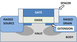
The device may comprise a Silicon On Insulator (SOI) device in which a Buried OXide (BOX) is formed below a thin semiconductor layer. If the channel region between the gate dielectric and a Buried Oxide (BOX) region is very thin, the very thin channel region is referred to as an Ultra Thin Channel (UTC) region with the source and drain regions formed on either side thereof in and/or above the thin semiconductor layer. Alternatively, the device may comprise a SEMiconductor On Insulator (SEMOI) device in which semiconductors other than silicon are employed. Many alternative semiconductor materials may be employed.
When the source and drain regions are formed above the channel in whole or in part, they are referred to as Raised Source/Drain (RSD) regions.
Modes of operation
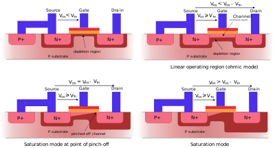
The operation of a MOSFET can be separated into three different modes, depending on the voltages at the terminals. In the following discussion, a simplified algebraic model is used that is accurate only for old technology. Modern MOSFET characteristics require computer models that have rather more complex behavior.For an enhancement-mode, n-channel MOSFET, the three operational modes are:
Cutoff, subthreshold, or weak-inversion mode
- When VGS < Vth:
- where
 is the threshold voltageThreshold voltageThe threshold voltage of a MOSFET is usually defined as the gate voltage where an inversion layer forms at the interface between the insulating layer and the substrate of the transistor. The purpose of the inversion layer's forming is to allow the flow of electrons through the gate-source junction...
of the device.
- where
- According to the basic threshold model, the transistor is turned off, and there is no conduction between drain and source. In reality, the Boltzmann distributionBoltzmann distributionIn chemistry, physics, and mathematics, the Boltzmann distribution is a certain distribution function or probability measure for the distribution of the states of a system. It underpins the concept of the canonical ensemble, providing its underlying distribution...
of electron energies allows some of the more energetic electrons at the source to enter the channel and flow to the drain, resulting in a subthreshold current that is an exponential function of gate–source voltage. While the current between drain and source should ideally be zero when the transistor is being used as a turned-off switch, there is a weak-inversion current, sometimes called subthreshold leakage. - In weak inversion the current varies exponentially with gate-to-source bias
 as given approximately by:
-
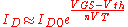 ,
,
- where
 = current at
  , the thermal voltage
  and the slope factor n is given by
-
 ,
,
- with
 = capacitance of the depletion layer and
  = capacitance of the oxide layer. In a long-channel device, there is no drain voltage dependence of the current once
  , but as channel length is reduced drain-induced barrier lowering introduces drain voltage dependence that depends in a complex way upon the device geometry (for example, the channel doping, the junction doping and so on). Frequently, threshold voltage Vth for this mode is defined as the gate voltage at which a selected value of current ID0 occurs, for example, ID0 = 1 μA, which may not be the same Vth-value used in the equations for the following modes.
- Some micropower analog circuits are designed to take advantage of subthreshold conduction. By working in the weak-inversion region, the MOSFETs in these circuits deliver the highest possible transconductance-to-current ratio, namely:
 , almost that of a bipolar transistor.
- The subthreshold I–V curve depends exponentially upon threshold voltage, introducing a strong dependence on any manufacturing variation that affects threshold voltage; for example: variations in oxide thickness, junction depth, or body doping that change the degree of drain-induced barrier lowering. The resulting sensitivity to fabricational variations complicates optimization for leakage and performance.


- When VGS > Vth and VDS < ( VGS – Vth )
- The transistor is turned on, and a channel has been created which allows current to flow between the drain and the source. The MOSFET operates like a resistor, controlled by the gate voltage relative to both the source and drain voltages. The current from drain to source is modeled as:
-
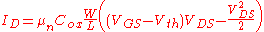
- where
 is the charge-carrier effective mobility,
  is the gate width,
  is the gate length and
  is the gate oxide capacitance per unit area. The transition from the exponential subthreshold region to the triode region is not as sharp as the equations suggest.
Saturation or active mode
- When VGS > Vth and VDS > ( VGS – Vth )
- The switch is turned on, and a channel has been created, which allows current to flow between the drain and source. Since the drain voltage is higher than the gate voltage, the electrons spread out, and conduction is not through a narrow channel but through a broader, two- or three-dimensional current distribution extending away from the interface and deeper in the substrate. The onset of this region is also known as pinch-off to indicate the lack of channel region near the drain. The drain current is now weakly dependent upon drain voltage and controlled primarily by the gate–source voltage, and modeled approximately as:
-

- The additional factor involving λ, the channel-length modulation parameter, models current dependence on drain voltage due to the Early effectEarly EffectThe Early effect is the variation in the width of the base in a bipolar junction transistor due to a variation in the applied base-to-collector voltage, named after its discoverer James M. Early...
, or channel length modulationChannel length modulationOne of several short channel effects in MOSFET scaling, channel length modulation is a shortening of the length of the inverted channel region with increase in drain bias for large drain biases...
. According to this equation, a key design parameter, the MOSFET transconductance is: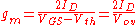 ,
,
- where the combination Vov = VGS – Vth is called the overdrive voltage, and where VDSsat = VGS - Vth (which Sedra neglects) accounts for a small discontinuity in
 which would otherwise appear at the transition between the triode and saturation regions.
 - Another key design parameter is the MOSFET output resistance rout given by:
 .
.- rout is the inverse of gDS where
 . VDS is the expression in saturation region.
- If λ is taken as zero, an infinite output resistance of the device results that leads to unrealistic circuit predictions, particularly in analog circuits.
- As the channel length becomes very short, these equations become quite inaccurate. New physical effects arise. For example, carrier transport in the active mode may become limited by velocity saturationVelocity saturationIn semiconductors, when a strong enough electric field is applied, the carrier velocity in the semiconductor reaches a maximum value, saturation velocity. When this happens, the semiconductor is said to be in a state of velocity saturation...
. When velocity saturation dominates, the saturation drain current is more nearly linear than quadratic in VGS. At even shorter lengths, carriers transport with near zero scattering, known as quasi-ballistic transportBallistic transportBallistic transport is the transport of electrons in a medium with negligible electrical resistivity due to scattering. Without scattering, electrons simply obey Newton's second law of motion at non-relativistic speeds....
. In addition, the output current is affected by drain-induced barrier lowering of the threshold voltage.
Body effect
-
 ,
,
where VTN is the threshold voltage with substrate bias present, and VTO is the zero-
 value of threshold voltage,
  is the body effect parameter, and
  is the surface potential
Volt
The volt is the SI derived unit for electric potential, electric potential difference, and electromotive force. The volt is named in honor of the Italian physicist Alessandro Volta , who invented the voltaic pile, possibly the first chemical battery.- Definition :A single volt is defined as the...
parameter.
The body can be operated as a second gate, and is sometimes referred to as the "back gate"; the body effect is sometimes called the "back-gate effect".
History
In 1959, Dawon Kahng and Martin M. (John) Atalla at Bell LabsBell Labs
Bell Laboratories is the research and development subsidiary of the French-owned Alcatel-Lucent and previously of the American Telephone & Telegraph Company , half-owned through its Western Electric manufacturing subsidiary.Bell Laboratories operates its...
invented the metal–oxide–semiconductor field-effect transistor (MOSFET) as an offshoot to the patented FET design.
Operationally and structurally different from the bipolar junction transistor,
the MOSFET was made by putting an insulating layer on the surface of the semiconductor and then placing a metallic gate electrode on that. It used crystalline silicon for the semiconductor and a thermally oxidized layer of silicon dioxide
Silicon dioxide
The chemical compound silicon dioxide, also known as silica , is an oxide of silicon with the chemical formula '. It has been known for its hardness since antiquity...
for the insulator. The silicon MOSFET did not generate localized electron traps at the interface between the silicon and its native oxide layer, and thus was inherently free from the trapping and scattering of carriers that had impeded the performance of earlier field-effect transistors. Following the (expensive) development of clean rooms to reduce contamination to levels never before thought necessary, and of photolithography
Photolithography
Photolithography is a process used in microfabrication to selectively remove parts of a thin film or the bulk of a substrate. It uses light to transfer a geometric pattern from a photomask to a light-sensitive chemical "photoresist", or simply "resist," on the substrate...
and the planar process
Planar process
The planar process is a manufacturing process used in the semiconductor industry to build individual components of a transistor, and in turn, connect those transistors together. It is the primary process by which modern integrated circuits are built...
to allow circuits to be made in very few steps, the Si–SiO2 system possessed such technical attractions as low cost of production (on a per circuit basis) and ease of integration. Largely because of these two factors, the MOSFET has become the most widely used type of transistor in integrated circuits.
CMOS circuits
The MOSFET is used in digital complementary metal–oxide–semiconductor (CMOSCMOS
Complementary metal–oxide–semiconductor is a technology for constructing integrated circuits. CMOS technology is used in microprocessors, microcontrollers, static RAM, and other digital logic circuits...
) logic, which uses p- and n-channel MOSFETs as building blocks. Overheating is a major concern in integrated circuit
Integrated circuit
An integrated circuit or monolithic integrated circuit is an electronic circuit manufactured by the patterned diffusion of trace elements into the surface of a thin substrate of semiconductor material...
s since ever more transistors are packed into ever smaller chips. CMOS logic reduces power consumption because no current flows (ideally), and thus no power
Power (physics)
In physics, power is the rate at which energy is transferred, used, or transformed. For example, the rate at which a light bulb transforms electrical energy into heat and light is measured in watts—the more wattage, the more power, or equivalently the more electrical energy is used per unit...
is consumed, except when the inputs to logic gate
Logic gate
A logic gate is an idealized or physical device implementing a Boolean function, that is, it performs a logical operation on one or more logic inputs and produces a single logic output. Depending on the context, the term may refer to an ideal logic gate, one that has for instance zero rise time and...
s are being switched. CMOS accomplishes this current reduction by complementing every nMOSFET with a pMOSFET and connecting both gates and both drains together. A high voltage on the gates will cause the nMOSFET to conduct and the pMOSFET not to conduct and a low voltage on the gates causes the reverse. During the switching time as the voltage goes from one state to another, both MOSFETs will conduct briefly. This arrangement greatly reduces power consumption and heat generation. Digital and analog CMOS applications are described below.
Digital
The growth of digital technologies like the microprocessorMicroprocessor
A microprocessor incorporates the functions of a computer's central processing unit on a single integrated circuit, or at most a few integrated circuits. It is a multipurpose, programmable device that accepts digital data as input, processes it according to instructions stored in its memory, and...
has provided the motivation to advance MOSFET technology faster than any other type of silicon-based transistor. A big advantage of MOSFETs for digital switching is that the oxide layer between the gate and the channel prevents DC current from flowing through the gate, further reducing power consumption and giving a very large input impedance. The insulating oxide between the gate and channel effectively isolates a MOSFET in one logic stage from earlier and later stages, which allows a single MOSFET output to drive a considerable number of MOSFET inputs. Bipolar transistor-based logic (such as TTL) does not have such a high fanout capacity. This isolation also makes it easier for the designers to ignore to some extent loading effects between logic stages independently. That extent is defined by the operating frequency: as frequencies increase, the input impedance of the MOSFETs decreases.
Analog
The MOSFET's advantages in digital circuits do not translate into supremacy in all analog circuits. The two types of circuit draw upon different features of transistor behavior. Digital circuits switch, spending most of their time outside the switching region, while analog circuits depend on MOSFET behavior held precisely in the switching region of operation. The bipolar junction transistorBipolar junction transistor
|- align = "center"| || PNP|- align = "center"| || NPNA bipolar transistor is a three-terminal electronic device constructed of doped semiconductor material and may be used in amplifying or switching applications. Bipolar transistors are so named because their operation involves both electrons...
(BJT) has traditionally been the analog designer's transistor of choice, due largely to its higher transconductance
Transconductance
Transconductance, also known as mutual conductance, is a property of certain electronic components. Conductance is the reciprocal of resistance; transconductance, meanwhile, is the ratio of the current change at the output port to the voltage change at the input port. It is written as gm...
and its lower output impedance
Output impedance
The output impedance, source impedance, or internal impedance of an electronic device is the opposition exhibited by its output terminals to an alternating current of a particular frequency as a result of resistance, inductance and capacitance...
(drain-voltage independence) in the switching region.
Nevertheless, MOSFETs are widely used in many types of analog circuits because of certain advantages. The characteristics and performance of many analog circuits can be designed by changing the sizes (length and width) of the MOSFETs used. By comparison, in most bipolar transistors the size of the device does not significantly affect the performance. MOSFETs' ideal characteristics regarding gate current (zero) and drain-source offset voltage (zero) also make them nearly ideal switch elements, and also make switched capacitor
Switched capacitor
A switched capacitor is an electronic circuit element used for discrete time signal processing. It works by moving charges into and out of capacitors when switches are opened and closed. Usually, non-overlapping signals are used to control the switches, so that not all switches are closed...
analog circuits practical. In their linear region, MOSFETs can be used as precision resistors, which can have a much higher controlled resistance than BJTs. In high power circuits, MOSFETs sometimes have the advantage of not suffering from thermal runaway
Thermal runaway
Thermal runaway refers to a situation where an increase in temperature changes the conditions in a way that causes a further increase in temperature, often leading to a destructive result...
as BJTs do. Also, they can be formed into capacitors and gyrator circuits
Gyrator
A gyrator is a passive, linear, lossless, two-port electrical network element proposed in 1948 by Tellegen as a hypothetical fifth linear element after the resistor, capacitor, inductor and ideal transformer. Unlike the four conventional elements, the gyrator is non-reciprocal...
which allow op-amps made from them to appear as inductors, thereby allowing all of the normal analog devices, except for diodes (which can be made smaller than a MOSFET anyway), to be built entirely out of MOSFETs. This allows for complete analog circuits to be made on a silicon chip in a much smaller space.
Some ICs combine analog and digital MOSFET circuitry on a single mixed-signal integrated circuit
Mixed-signal integrated circuit
A mixed-signal integrated circuit is any integrated circuit that has both analog circuits and digital circuits on a single semiconductor die.- Examples :...
, making the needed board space even smaller. This creates a need to isolate the analog circuits from the digital circuits on a chip level, leading to the use of isolation rings and Silicon-On-Insulator (SOI). The main advantage of BJTs versus MOSFETs in the analog design process is the ability of BJTs to handle a larger current in a smaller space. Fabrication processes exist that incorporate BJTs and MOSFETs into a single device. Mixed-transistor devices are called Bi-FETs (Bipolar-FETs) if they contain just one BJT-FET and BiCMOS
BiCMOS
BiCMOS is an evolved semiconductor technology that integrates two formerly separate semiconductor technologies - those of the analog bipolar junction transistor and the digital CMOS transistor - in a single integrated circuit device....
(bipolar-CMOS) if they contain complementary BJT-FETs. Such devices have the advantages of both insulated gates and higher current density.
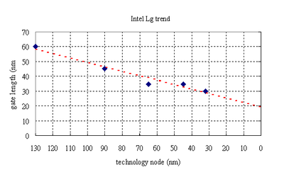
MOSFET scaling
Over the past decades, the MOSFET has continually been scaled down in size; typical MOSFET channel lengths were once several micrometreMicrometre
A micrometer , is by definition 1×10⁻⁶ of a meter .In plain English, it means one-millionth of a meter . Its unit symbol in the International System of Units is μm...
s, but modern integrated circuits are incorporating MOSFETs with channel lengths of tens of nanometers. Robert Dennard's work on scaling theory was pivotal in recognising that this ongoing reduction was possible. Intel began production of a process featuring a 32 nm feature size (with the channel being even shorter) in late 2009. The semiconductor industry maintains a "roadmap", the ITRS, which sets the pace for MOSFET development. Historically, the difficulties with decreasing the size of the MOSFET have been associated with the semiconductor device fabrication process, the need to use very low voltages, and with poorer electrical performance necessitating circuit redesign and innovation (small MOSFETs exhibit higher leakage currents, and lower output resistance, discussed below).
Reasons for MOSFET scaling
Smaller MOSFETs are desirable for several reasons. The main reason to make transistors smaller is to pack more and more devices in a given chip area. This results in a chip with the same functionality in a smaller area, or chips with more functionality in the same area. Since fabrication costs for a semiconductor waferWafer (electronics)
A wafer is a thin slice of semiconductor material, such as a silicon crystal, used in the fabrication of integrated circuits and other microdevices...
are relatively fixed, the cost per integrated circuits is mainly related to the number of chips that can be produced per wafer. Hence, smaller ICs allow more chips per wafer, reducing the price per chip. In fact, over the past 30 years the number of transistors per chip has been doubled every 2–3 years once a new technology node is introduced. For example the number of MOSFETs in a microprocessor fabricated in a 45 nm technology is twice as many as in a 65 nm chip. This doubling of the transistor count was first observed by Gordon Moore
Gordon Moore
Gordon Earle Moore is the co-founder and Chairman Emeritus of Intel Corporation and the author of Moore's Law .-Life and career:...
in 1965 and is commonly referred to as Moore's law
Moore's Law
Moore's law describes a long-term trend in the history of computing hardware: the number of transistors that can be placed inexpensively on an integrated circuit doubles approximately every two years....
.
While this has been traditionally the case for the older technologies, for the state-of-the-art MOSFETs reduction of the transistor dimensions does not necessarily translate to higher chip speed because the delay due to interconnections is more significant.
Difficulties arising due to MOSFET size reduction
Producing MOSFETs with channel lengths much smaller than a micrometreMicrometre
A micrometer , is by definition 1×10⁻⁶ of a meter .In plain English, it means one-millionth of a meter . Its unit symbol in the International System of Units is μm...
is a challenge, and the difficulties of semiconductor device fabrication are always a limiting factor in advancing integrated circuit technology. In recent years, the small size of the MOSFET, below a few tens of nanometers, has created operational problems.
Higher subthreshold conduction
As MOSFET geometries shrink, the voltage that can be applied to the gate must be reduced to maintain reliability. To maintain performance, the threshold voltage of the MOSFET has to be reduced as well. As threshold voltage is reduced, the transistor cannot be switched from complete turn-off to complete turn-on with the limited voltage swing available; the circuit design is a compromise between strong current in the "on" case and low current in the "off" case, and the application determines whether to favor one over the other. Subthreshold leakage (including subthreshold conduction, gate-oxide leakage and reverse-biased junction leakage), which was ignored in the past, now can consume upwards of half of the total power consumption of modern high-performance VLSI chips.Increased gate-oxide leakage
The gate oxide, which serves as insulator between the gate and channel, should be made as thin as possible to increase the channel conductivity and performance when the transistor is on and to reduce subthreshold leakage when the transistor is off. However, with current gate oxides with a thickness of around 1.2 nm (which in silicon is ~5 atomAtom
The atom is a basic unit of matter that consists of a dense central nucleus surrounded by a cloud of negatively charged electrons. The atomic nucleus contains a mix of positively charged protons and electrically neutral neutrons...
s thick) the quantum mechanical
Quantum mechanics
Quantum mechanics, also known as quantum physics or quantum theory, is a branch of physics providing a mathematical description of much of the dual particle-like and wave-like behavior and interactions of energy and matter. It departs from classical mechanics primarily at the atomic and subatomic...
phenomenon of electron tunneling occurs between the gate and channel, leading to increased power consumption.
Insulators that have a larger dielectric constant
Dielectric constant
The relative permittivity of a material under given conditions reflects the extent to which it concentrates electrostatic lines of flux. In technical terms, it is the ratio of the amount of electrical energy stored in a material by an applied voltage, relative to that stored in a vacuum...
than silicon dioxide (referred to as high-k dielectrics
High-k Dielectric
The term high-κ dielectric refers to a material with a high dielectric constant κ used in semiconductor manufacturing processes which replaces the silicon dioxide gate dielectric...
), such as group IVb metal silicates e.g. hafnium
Hafnium
Hafnium is a chemical element with the symbol Hf and atomic number 72. A lustrous, silvery gray, tetravalent transition metal, hafnium chemically resembles zirconium and is found in zirconium minerals. Its existence was predicted by Dmitri Mendeleev in 1869. Hafnium was the penultimate stable...
and zirconium
Zirconium
Zirconium is a chemical element with the symbol Zr and atomic number 40. The name of zirconium is taken from the mineral zircon. Its atomic mass is 91.224. It is a lustrous, grey-white, strong transition metal that resembles titanium...
silicates and oxides are being used to reduce the gate leakage from the 45 nanometer technology node onwards. Increasing the dielectric constant of the gate dielectric allows a thicker layer while maintaining a high capacitance (capacitance is proportional to dielectric constant and inversely proportional to dielectric thickness). All else equal, a higher dielectric thickness reduces the quantum tunneling current through the dielectric between the gate and the channel. On the other hand, the barrier height of the new gate insulator is an important consideration; the difference in conduction band
Conduction band
In the solid-state physics field of semiconductors and insulators, the conduction band is the range of electron energies, higher than that of the valence band, sufficient to free an electron from binding with its individual atom and allow it to move freely within the atomic lattice of the material...
energy between the semiconductor and the dielectric (and the corresponding difference in valence band
Valence band
In solids, the valence band is the highest range of electron energies in which electrons are normally present at absolute zero temperature....
energy) also affects leakage current level. For the traditional gate oxide, silicon dioxide, the former barrier is approximately 8 eV
Electronvolt
In physics, the electron volt is a unit of energy equal to approximately joule . By definition, it is equal to the amount of kinetic energy gained by a single unbound electron when it accelerates through an electric potential difference of one volt...
. For many alternative dielectrics the value is significantly lower, tending to increase the tunneling current, somewhat negating the advantage of higher dielectric constant.
Increased junction leakage
To make devices smaller, junction design has become more complex, leading to higher doping levels, shallower junctions, "halo" doping and so forth, all to decrease drain-induced barrier lowering (see the section on junction design). To keep these complex junctions in place, the annealing steps formerly used to remove damage and electrically active defects must be curtailed increasing junction leakage. Heavier doping is also associated with thinner depletion layers and more recombination centers that result in increased leakage current, even without lattice damage.Lower output resistance
For analog operation, good gain requires a high MOSFET output impedance, which is to say, the MOSFET current should vary only slightly with the applied drain-to-source voltage. As devices are made smaller, the influence of the drain competes more successfully with that of the gate due to the growing proximity of these two electrodes, increasing the sensitivity of the MOSFET current to the drain voltage. To counteract the resulting decrease in output resistance, circuits are made more complex, either by requiring more devices, for example the cascodeCascode
The cascode is a two-stage amplifier composed of a transconductance amplifier followed by a current buffer. Compared to a single amplifier stage, this combination may have one or more of the following characteristics: higher input-output isolation, higher input impedance, high output impedance,...
and cascade amplifier
Cascade amplifier
A cascade amplifier is any amplifier constructed from a series of amplifiers, where each amplifier sends its output to the input of the next amplifier in a daisy chain....
s, or by feedback circuitry using operational amplifiers, for example a circuit like that in the adjacent figure.
Lower transconductance
The transconductanceTransconductance
Transconductance, also known as mutual conductance, is a property of certain electronic components. Conductance is the reciprocal of resistance; transconductance, meanwhile, is the ratio of the current change at the output port to the voltage change at the input port. It is written as gm...
of the MOSFET decides its gain and is proportional to hole or electron mobility
Electron mobility
In solid-state physics, the electron mobility characterizes how quickly an electron can move through a metal or semiconductor, when pulled by an electric field. In semiconductors, there is an analogous quantity for holes, called hole mobility...
(depending on device type), at least for low drain voltages. As MOSFET size is reduced, the fields in the channel increase and the dopant impurity levels increase. Both changes reduce the carrier mobility, and hence the transconductance. As channel lengths are reduced without proportional reduction in drain voltage, raising the electric field in the channel, the result is velocity saturation of the carriers, limiting the current and the transconductance.
Interconnect capacitance
Traditionally, switching time was roughly proportional to the gate capacitance of gates. However, with transistors becoming smaller and more transistors being placed on the chip, interconnect capacitanceCapacitance
In electromagnetism and electronics, capacitance is the ability of a capacitor to store energy in an electric field. Capacitance is also a measure of the amount of electric potential energy stored for a given electric potential. A common form of energy storage device is a parallel-plate capacitor...
(the capacitance of the metal-layer connections between different parts of the chip) is becoming a large percentage of capacitance.
Signals have to travel through the interconnect, which leads to increased delay and lower performance.
Heat production
The ever-increasing density of MOSFETs on an integrated circuit creates problems of substantial localized heat generation that can impair circuit operation. Circuits operate slower at high temperatures, and have reduced reliability and shorter lifetimes. Heat sinks and other cooling methods are now required for many integrated circuits including microprocessors.Power MOSFETs are at risk of thermal runaway. As their on-state resistance rises with temperature, if the load is approximately a constant-current load then the power loss rises correspondingly, generating further heat. When the heatsink is not able to keep the temperature low enough, the junction temperature may rise quickly and uncontrollably, resulting in destruction of the device.
Process variations
With MOSFETS becoming smaller, the number of atoms in the silicon that produce many of the transistor's properties is becoming fewer, with the result that control of dopant numbers and placement is more erratic. During chip manufacturing, random process variations affect all transistor dimensions: length, width, junction depths, oxide thickness etc., and become a greater percentage of overall transistor size as the transistor shrinks. The transistor characteristics become less certain, more statistical. The random nature of manufacture means we do not know which particular example MOSFETs actually will end up in a particular instance of the circuit. This uncertainty forces a less optimal design because the design must work for a great variety of possible component MOSFETs. See process variationProcess variation (semiconductor)
Process variation is the naturally occurring variation the attributes of transistors when integrated circuits are fabricated. It becomes particularly important at smaller process nodes Process variation is the naturally occurring variation the attributes of transistors (length, widths, oxide...
, design for manufacturability
Design for manufacturability (IC)
Achieving high-yielding designs in the state of the art, VLSI technology has become an extremely challenging task due to the miniaturization as well as the complexity of leading-edge products...
, reliability engineering
Reliability engineering
Reliability engineering is an engineering field, that deals with the study, evaluation, and life-cycle management of reliability: the ability of a system or component to perform its required functions under stated conditions for a specified period of time. It is often measured as a probability of...
, and statistical process control
Statistical process control
Statistical process control is the application of statistical methods to the monitoring and control of a process to ensure that it operates at its full potential to produce conforming product. Under SPC, a process behaves predictably to produce as much conforming product as possible with the least...
.
Modeling challenges
Modern ICs are computer-simulated with the goal of obtaining working circuits from the very first manufactured lot. As devices are miniaturized, the complexity of the processing makes it difficult to predict exactly what the final devices look like, and modeling of physical processes becomes more challenging as well. In addition, microscopic variations in structure due simply to the probabilistic nature of atomic processes require statistical (not just deterministic) predictions. These factors combine to make adequate simulation and "right the first time" manufacture difficult.Gate material
The primary criterion for the gate material is that it is a good conductor. Highly doped polycrystalline siliconPolycrystalline silicon
Polycrystalline silicon, also called polysilicon, is a material consisting of small silicon crystals. It differs from single-crystal silicon, used for electronics and solar cells, and from amorphous silicon, used for thin film devices and solar cells....
is an acceptable but certainly not ideal conductor, and also suffers from some more technical deficiencies in its role as the standard gate material. Nevertheless, there are several reasons favoring use of polysilicon:
- The threshold voltageThreshold voltageThe threshold voltage of a MOSFET is usually defined as the gate voltage where an inversion layer forms at the interface between the insulating layer and the substrate of the transistor. The purpose of the inversion layer's forming is to allow the flow of electrons through the gate-source junction...
(and consequently the drain to source on-current) is modified by the work functionWork functionIn solid-state physics, the work function is the minimum energy needed to remove an electron from a solid to a point immediately outside the solid surface...
difference between the gate material and channel material. Because polysilicon is a semiconductor, its work function can be modulated by adjusting the type and level of doping. Furthermore, because polysilicon has the same bandgap as the underlying silicon channel, it is quite straightforward to tune the work function to achieve low threshold voltages for both NMOS and PMOS devices. By contrast, the work functions of metals are not easily modulated, so tuning the work functionWork functionIn solid-state physics, the work function is the minimum energy needed to remove an electron from a solid to a point immediately outside the solid surface...
to obtain low threshold voltages becomes a significant challenge. Additionally, obtaining low-threshold devices on both PMOS and NMOS devices would likely require the use of different metals for each device type, introducing additional complexity to the fabrication process. - The silicon-SiO2 interface has been well studied and is known to have relatively few defects. By contrast many metal–insulator interfaces contain significant levels of defects which can lead to Fermi levelFermi levelThe Fermi level is a hypothetical level of potential energy for an electron inside a crystalline solid. Occupying such a level would give an electron a potential energy \epsilon equal to its chemical potential \mu as they both appear in the Fermi-Dirac distribution function,which...
pinning, charging, or other phenomena that ultimately degrade device performance. - In the MOSFET IC fabrication process, it is preferable to deposit the gate material prior to certain high-temperature steps in order to make better-performing transistors. Such high temperature steps would melt some metals, limiting the types of metal that can be used in a metal-gate-based process.
While polysilicon gates have been the de facto standard for the last twenty years, they do have some disadvantages which have led to their likely future replacement by metal gates. These disadvantages include:
- Polysilicon is not a great conductor (approximately 1000 times more resistive than metals) which reduces the signal propagation speed through the material. The resistivity can be lowered by increasing the level of doping, but even highly doped polysilicon is not as conductive as most metals. In order to improve conductivity further, sometimes a high-temperature metal such as tungstenTungstenTungsten , also known as wolfram , is a chemical element with the chemical symbol W and atomic number 74.A hard, rare metal under standard conditions when uncombined, tungsten is found naturally on Earth only in chemical compounds. It was identified as a new element in 1781, and first isolated as...
, titaniumTitaniumTitanium is a chemical element with the symbol Ti and atomic number 22. It has a low density and is a strong, lustrous, corrosion-resistant transition metal with a silver color....
, cobaltCobaltCobalt is a chemical element with symbol Co and atomic number 27. It is found naturally only in chemically combined form. The free element, produced by reductive smelting, is a hard, lustrous, silver-gray metal....
, and more recently nickelNickelNickel is a chemical element with the chemical symbol Ni and atomic number 28. It is a silvery-white lustrous metal with a slight golden tinge. Nickel belongs to the transition metals and is hard and ductile...
is alloyed with the top layers of the polysilicon. Such a blended material is called silicideSilicideA silicide is a compound that has silicon with more electropositive elements.Silicon is more electropositive than carbon. Silicides are structurally closer to borides than to carbides....
. The silicide-polysilicon combination has better electrical properties than polysilicon alone and still does not melt in subsequent processing. Also the threshold voltage is not significantly higher than with polysilicon alone, because the silicide material is not near the channel. The process in which silicide is formed on both the gate electrode and the source and drain regions is sometimes called salicideSalicideThe term salicide refers to a technology used in the microelectronics industry used to form electrical contacts between the semiconductor device and the supporting interconnect structure...
, self-aligned silicide. - When the transistors are extremely scaled down, it is necessary to make the gate dielectric layer very thin, around 1 nm in state-of-the-art technologies. A phenomenon observed here is the so-called poly depletion, where a depletion layer is formed in the gate polysilicon layer next to the gate dielectric when the transistor is in the inversion. To avoid this problem, a metal gate is desired. A variety of metal gates such as tantalumTantalumTantalum is a chemical element with the symbol Ta and atomic number 73. Previously known as tantalium, the name comes from Tantalus, a character in Greek mythology. Tantalum is a rare, hard, blue-gray, lustrous transition metal that is highly corrosion resistant. It is part of the refractory...
, tungsten, tantalum nitride, and titanium nitrideTitanium nitrideTitanium nitride is an extremely hard ceramic material, often used as a coating on titanium alloys, steel, carbide, and aluminium components to improve the substrate's surface properties....
are used, usually in conjunction with high-k dielectrics. An alternative is to use fully silicided polysilicon gates, a process known as FUSIFusiA. Fusi & Co., S.p.A. Milano is an historic brand of motorcycles.Achille Fusi was a trader of FN motorcycles. In 1932 he started building motorcycles under the RAS brand name, mainly with FN parts. They had 175 cc JAP engines made under licence in Italy and Burman gearboxes made under licence by...
.
Insulator
As devices are made smaller, insulating layers are made thinner, and at some point tunneling of carriers through the insulator from the channel to the gate electrode takes place. To reduce the resulting leakageLeakage (semiconductors)
In semiconductor devices, leakage is a quantum phenomenon where mobile charge carriers tunnel through an insulating region. Leakage increases exponentially as the thickness of the insulating region decreases. Tunneling leakage can also occur across semiconductor junctions between heavily doped...
current, the insulator can be made thicker by choosing a material with a higher dielectric constant. To see how thickness and dielectric constant are related, note that Gauss' law connects field to charge as:
-
 ,
,
with Q = charge density, κ = dielectric constant, ε0 = permittivity of empty space and E = electric field. From this law it appears the same charge can be maintained in the channel at a lower field provided κ is increased. The voltage on the gate is given by:
-
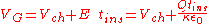 ,
,
with VG = gate voltage, Vch = voltage at channel side of insulator, and tins = insulator thickness. This equation shows the gate voltage will not increase when the insulator thickness increases, provided κ increases to keep tins /κ = constant (see the article on high-κ dielectrics for more detail, and the section in this article on gate-oxide leakage).
The insulator in a MOSFET is a dielectric which can in any event be silicon oxide, but many other dielectric materials are employed. The generic term for the dielectric is gate dielectric since the dielectric lies directly below the gate electrode and above the channel of the MOSFET.
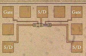
Junction design
The source-to-body and drain-to-body junctionsP-n junction
A p–n junction is formed at the boundary between a P-type and N-type semiconductor created in a single crystal of semiconductor by doping, for example by ion implantation, diffusion of dopants, or by epitaxy .If two separate pieces of material were used, this would...
are the object of much attention because of three major factors: their design affects the current-voltage (I-V) characteristics
Current-voltage characteristic
A current–voltage characteristic is a relationship, typically represented as a chart or graph, between an electric current and a corresponding voltage, or potential difference.-In electronics:...
of the device, lowering output resistance, and also the speed of the device through the loading effect of the junction capacitance
Capacitance
In electromagnetism and electronics, capacitance is the ability of a capacitor to store energy in an electric field. Capacitance is also a measure of the amount of electric potential energy stored for a given electric potential. A common form of energy storage device is a parallel-plate capacitor...
s, and finally, the component of stand-by power dissipation due to junction leakage.
Channel length modulation
One of several short channel effects in MOSFET scaling, channel length modulation is a shortening of the length of the inverted channel region with increase in drain bias for large drain biases...
effects upon I-V curves are reduced by using shallow junction extensions. In addition, halo doping can be used, that is, the addition of very thin heavily doped regions of the same doping type as the body tight against the junction walls to limit the extent of depletion region
Depletion region
In semiconductor physics, the depletion region, also called depletion layer, depletion zone, junction region or the space charge region, is an insulating region within a conductive, doped semiconductor material where the mobile charge carriers have diffused away, or have been forced away by an...
s.
The capacitive effects are limited by using raised source and drain geometries that make most of the contact area border thick dielectric instead of silicon.
These various features of junction design are shown (with artistic license
Artistic license
Artistic licence is a colloquial term, sometimes euphemism, used to denote the distortion of fact, alteration of the conventions of grammar or language, or rewording of pre-existing text made by an artist to improve a piece of...
) in the figure.
Junction leakage is discussed further in the section increased junction leakage.
Dual gate MOSFET
The dual gate MOSFET has a tetrodeTetrode
A tetrode is an electronic device having four active electrodes. The term most commonly applies to a two-grid vacuum tube. It has the three electrodes of a triode and an additional screen grid which significantly changes its behaviour.-Control grid:...
configuration, where both gates control the current in the device. It is commonly used for small signal devices in radio frequency applications where the second gate is normally used for gain control or mixing and frequency conversion.
FinFET
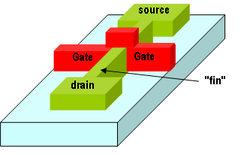
Multigate device
A multigate device or multiple gate field-effect transistor refers to a MOSFET which incorporates more than one gate into a single device. The multiple gates may be controlled by a single gate electrode, wherein the multiple gate surfaces act electrically as a single gate, or by independent gate...
, see figure to right, is a double gate device, one of a number of geometries being introduced to mitigate the effects of short channels and reduce drain-induced barrier lowering.
Depletion-mode MOSFETs
There are depletion-mode MOSFET devices, which are less commonly used than the standard enhancement-mode devices already described. These are MOSFET devices that are doped so that a channel exists even with zero voltage from gate to source. In order to control the channel, a negative voltage is applied to the gate (for an n-channel device), depleting the channel, which reduces the current flow through the device. In essence, the depletion-mode device is equivalent to a normally closed (on) switch, while the enhancement-mode device is equivalent to a normally open (off) switch.Due to their low noise figure in the RF region, and better gain, these devices are often preferred to bipolars in RF front-ends such as in TV sets. Depletion-mode MOSFET families include BF 960 by Siemens and BF 980 by Philips (dated 1980s), whose derivatives are still used in AGC and RF mixer front-ends.
NMOS logic
n-channel MOSFETs are smaller than p-channel MOSFETs and producing only one type of MOSFET on a silicon substrate is cheaper and technically simpler. These were the driving principles in the design of NMOS logicNMOS logic
N-type metal-oxide-semiconductor logic uses n-type metal-oxide-semiconductor field effect transistors to implement logic gates and other digital circuits...
which uses n-channel MOSFETs exclusively. However, unlike CMOS logic, NMOS logic consumes power even when no switching is taking place. With advances in technology, CMOS logic displaced NMOS logic in the mid 1980s to become the preferred process for digital chips.
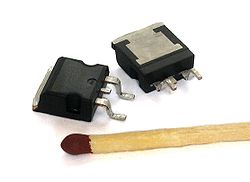
Power MOSFET
Power MOSFET
Power MOSFET
A Power MOSFET is a specific type of metal oxide semiconductor field-effect transistor designed to handle significant power levels. Compared to the other power semiconductor devices , its main advantages are high commutation speed and good efficiency at low voltages...
s have a different structure than the one presented above. As with most power devices, the structure is vertical and not planar. Using a vertical structure, it is possible for the transistor to sustain both high blocking voltage and high current. The voltage rating of the transistor is a function of the doping and thickness of the N-epitaxial
Epitaxy
Epitaxy refers to the deposition of a crystalline overlayer on a crystalline substrate, where the overlayer is in registry with the substrate. In other words, there must be one or more preferred orientations of the overlayer with respect to the substrate for this to be termed epitaxial growth. The...
layer (see cross section), while the current rating is a function of the channel width (the wider the channel, the higher the current). In a planar structure, the current and breakdown voltage ratings are both a function of the channel dimensions (respectively width and length of the channel), resulting in inefficient use of the "silicon estate". With the vertical structure, the component area is roughly proportional to the current it can sustain, and the component thickness (actually the N-epitaxial layer thickness) is proportional to the breakdown voltage.
Power MOSFETs with lateral structure are mainly used in high-end audio amplifiers and high-power PA systems. Their advantage is a better behaviour in the saturated region (corresponding to the linear region of a bipolar transistor) than the vertical MOSFETs. Vertical MOSFETs are designed for switching applications.
DMOS
DMOS stands for double-diffused metal–oxide–semiconductor. Most power MOSFETs are made using this technology.RHBD MOSFETs
Semiconductor sub-micrometer and nanometer electronic circuits are the primary concern for operating within the normal tolerance in harsh radiationRadiation
In physics, radiation is a process in which energetic particles or energetic waves travel through a medium or space. There are two distinct types of radiation; ionizing and non-ionizing...
environments like outer space
Outer space
Outer space is the void that exists between celestial bodies, including the Earth. It is not completely empty, but consists of a hard vacuum containing a low density of particles: predominantly a plasma of hydrogen and helium, as well as electromagnetic radiation, magnetic fields, and neutrinos....
. One of the design approaches for making a radiation-hardened-by-design
Radiation hardening
Radiation hardening is a method of designing and testing electronic components and systems to make them resistant to damage or malfunctions caused by ionizing radiation , such as would be encountered in outer space, high-altitude flight, around nuclear reactors, particle accelerators, or during...
(RHBD) device is Enclosed-Layout-Transistor (ELT). Normally, the gate of the MOSFET surrounds the drain, which is placed in the center of the ELT. The source of the MOSFET surrounds the gate. Another RHBD MOSFET is called H-Gate. Both of these transistors have very low leakage current with respect to radiation. However, they are large in size and take more space on silicon than a standard MOSFET.
Newer technologies are emerging for smaller devices for cost saving, low power and increased operating speed. The standard MOSFET is also becoming extremely sensitive to radiation for the newer technologies. A lot more research works should be completed before space electronics can safely use RHBD MOSFET circuits of nanotechnology.
When radiation strikes near the silicon oxide region (STI) of the MOSFET, the channel inversion occurs at the corners of the standard MOSFET due to accumulation of radiation induced trapped charges. If the charges are large enough, the accumulated charges affect STI surface edges along the channel near the channel interface (gate) of the standard MOSFET. Thus the device channel inversion occurs along the channel edges and the device creates off-state leakage path, causing device to turn on. So the reliability of circuits degrades severely. The ELT offers many advantages. These advantages include improvement of reliability
Reliability (semiconductor)
Reliability of semiconductor devices can be summarized as follows:# Semiconductor devices are very sensitive to impurities and particles. Therefore, to manufacture these devices it is necessary to manage many processes while accurately controlling the level of impurities and particles...
by reducing unwanted surface inversion at the gate edges that occurs in the standard MOSFET. Since the gate edges are enclosed in ELT, there is no gate oxide edge (STI at gate interface), and thus the transistor off-state leakage is reduced very much.
Low-power microelectronic circuits including computers, communication devices and monitoring systems in space shuttle and satellites are very different than what we use on earth. They are radiation (high-speed atomic particles like proton
Proton
The proton is a subatomic particle with the symbol or and a positive electric charge of 1 elementary charge. One or more protons are present in the nucleus of each atom, along with neutrons. The number of protons in each atom is its atomic number....
and neutron
Neutron
The neutron is a subatomic hadron particle which has the symbol or , no net electric charge and a mass slightly larger than that of a proton. With the exception of hydrogen, nuclei of atoms consist of protons and neutrons, which are therefore collectively referred to as nucleons. The number of...
, solar flare
Solar flare
A solar flare is a sudden brightening observed over the Sun surface or the solar limb, which is interpreted as a large energy release of up to 6 × 1025 joules of energy . The flare ejects clouds of electrons, ions, and atoms through the corona into space. These clouds typically reach Earth a day...
magnetic energy dissipation in earth's space, energetic cosmic rays like X-ray
X-ray
X-radiation is a form of electromagnetic radiation. X-rays have a wavelength in the range of 0.01 to 10 nanometers, corresponding to frequencies in the range 30 petahertz to 30 exahertz and energies in the range 120 eV to 120 keV. They are shorter in wavelength than UV rays and longer than gamma...
, gamma ray
Gamma ray
Gamma radiation, also known as gamma rays or hyphenated as gamma-rays and denoted as γ, is electromagnetic radiation of high frequency . Gamma rays are usually naturally produced on Earth by decay of high energy states in atomic nuclei...
etc.) tolerant circuits. These special electronics are designed by applying very different techniques using RHBD MOSFETs to ensure the safe space journey and also space-walk of astronauts.
MOSFET analog switch
MOSFET analog switches use the MOSFET channel as a low–on-resistance switch to pass analog signals when on, and as a high impedance when off. Signals flow in both directions across a MOSFET switch. In this application, the drain and source of a MOSFET exchange places depending on the relative voltages of the source/drain electrodes. The source is the more negative side for an N-MOS or the more positive side for a P-MOS. All of these switches are limited on what signals they can pass or stop by their gate–source, gate–drain and source–drain voltages; exceeding the voltage, current, or power limits will potentially damage the switch.Single-type MOSFET switch
This analog switch uses a four-terminal simple MOSFET of either P or N type. In the case of an N-type switch, the body is connected to the most negative supply (usually GND) and the gate is used as the switch control. Whenever the gate voltage exceeds the source voltage by at least a threshold voltage, the MOSFET conducts. The higher the voltage, the more the MOSFET can conduct. An N-MOS switch passes all voltages less than Vgate–Vtn. When the switch is conducting, it typically operates in the linear (or ohmic) mode of operation, since the source and drain voltages will typically be nearly equal.In the case of a P-MOS, the body is connected to the most positive voltage, and the gate is brought to a lower potential to turn the switch on. The P-MOS switch passes all voltages higher than Vgate–Vtp (threshold voltage Vtp is negative in the case of enhancent-mode P-MOS).
A P-MOS switch will have about three times the resistance of an N-MOS device of equal dimensions because electrons have about three times the mobility of holes in silicon.
Dual-type (CMOS) MOSFET switch
This "complementary" or CMOS type of switch uses one P-MOS and one N-MOS FET to counteract the limitations of the single-type switch. The FETs have their drains and sources connected in parallel, the body of the P-MOS is connected to the high potential (VDD) and the body of the N-MOS is connected to the low potential (Gnd). To turn the switch on, the gate of the P-MOS is driven to the low potential and the gate of the N-MOS is driven to the high potential. For voltages between VDD–Vtn and Gnd–Vtp, both FETs conduct the signal; for voltages less than Gnd–Vtp, the N-MOS conducts alone; and for voltages greater than VDD–Vtn, the P-MOS conducts alone.The voltage limits for this switch are the gate–source, gate–drain and source–drain voltage limits for both FETs. Also, the P-MOS is typically two to three times wider than the N-MOS, so the switch will be balanced for speed in the two directions.
Tri-state circuitry
Three-state logic
In digital electronics three-state, tri-state, or 3-state logic allows an output port to assume a high impedance state in addition to the 0 and 1 logic levels, effectively removing the output from the circuit...
sometimes incorporates a CMOS MOSFET switch on its output to provide for a low-ohmic, full-range output when on, and a high-ohmic, mid-level signal when off.
External links
- Dr. Ulrich Nicolai, Dr. Tobias Reimann, Prof. Jürgen Petzoldt, Josef Lutz: Application Manual IGBT and MOSFET Power Modules, 1. Edition, ISLE Verlag, 1998, ISBN 3-932633-24-5 PDF-Version
- An introduction to depletion-mode MOSFETs
- Power MOSFETs
- MOSFET Process Step by Step A Flash slide showing the fabricating process of a MOSFET in detail step
- MOSFET Calculator MOSFET Calculator
- Advanced MOSFET Issues Advanced MOSFET issues. Ece-www.colorado.edu. Retrieved on 2010-11-27.
- MOSFET applet Very nice applet that helps to understand MOSFET.
- MIT OpenCourseWare courses:
- MIT Open Courseware 6.002 – Spring 2007 – Link to the intro electrical engineering course at MIT on circuits and electronics.
- MIT Open Courseware 6.012 – Fall 2005 – Link to a more advanced class taught at MIT all about microelectronics and MOSFETs
- Georgia Tech BJT and FET Slides Slides from a Microelectronic Circuits class at Georgia Tech
- CircuitDesign: MOS Diffusion Parasitics Crude illustrations of MOS diffusion structure and sample circuit layouts to minimize their parasitics
- Course on Physics of Nanoscale Transistors
- Notes on Ballistic MOSFETs by Dr. Lundstrom – theory of ballistic MOSFETs.