

Field-effect transistor
Encyclopedia

Transistor
A transistor is a semiconductor device used to amplify and switch electronic signals and power. It is composed of a semiconductor material with at least three terminals for connection to an external circuit. A voltage or current applied to one pair of the transistor's terminals changes the current...
that relies on an electric field
Electric field
In physics, an electric field surrounds electrically charged particles and time-varying magnetic fields. The electric field depicts the force exerted on other electrically charged objects by the electrically charged particle the field is surrounding...
to control the shape and hence the conductivity of a channel of one type of charge carrier
Charge carrier
In physics, a charge carrier is a free particle carrying an electric charge, especially the particles that carry electric currents in electrical conductors. Examples are electrons and ions...
in a semiconductor
Semiconductor
A semiconductor is a material with electrical conductivity due to electron flow intermediate in magnitude between that of a conductor and an insulator. This means a conductivity roughly in the range of 103 to 10−8 siemens per centimeter...
material. FETs are sometimes called unipolar transistors to contrast their single-carrier-type operation with the dual-carrier-type operation of bipolar (junction) transistor
Bipolar junction transistor
|- align = "center"| || PNP|- align = "center"| || NPNA bipolar transistor is a three-terminal electronic device constructed of doped semiconductor material and may be used in amplifying or switching applications. Bipolar transistors are so named because their operation involves both electrons...
s (BJT). The concept of the FET predates the BJT, though it was not physically implemented until after BJTs due to the limitations of semiconductor materials and the relative ease of manufacturing BJTs compared to FETs at the time.
History
The principle of field-effect transistors was first patented by Julius Edgar LilienfeldJulius Edgar Lilienfeld
Julius Edgar Lilienfeld was an Austro-Hungarian physicist. He was born in Lemberg in Austria-Hungary , moved to the United States in the early 1920s, and became American citizen in 1934...
in 1925 and by Oskar Heil
Oskar Heil
Oskar Heil was a German electrical engineer and inventor. He studied physics, chemistry, mathematics, and music at the Georg-August University of Göttingen and was awarded his PhD in 1933, for his work on molecular spectroscopy.-Personal life:At the Georg-August University in Göttingen, Oskar Heil...
in 1934, but practical semi-conducting devices (the JFET
JFET
The junction gate field-effect transistor is the simplest type of field-effect transistor. It can be used as an electronically-controlled switch or as a voltage-controlled resistance. Electric charge flows through a semiconducting channel between "source" and "drain" terminals...
, junction gate field-effect transistor) were only developed much later after the transistor
Transistor
A transistor is a semiconductor device used to amplify and switch electronic signals and power. It is composed of a semiconductor material with at least three terminals for connection to an external circuit. A voltage or current applied to one pair of the transistor's terminals changes the current...
effect was observed and explained by the team of William Shockley
William Shockley
William Bradford Shockley Jr. was an American physicist and inventor. Along with John Bardeen and Walter Houser Brattain, Shockley co-invented the transistor, for which all three were awarded the 1956 Nobel Prize in Physics.Shockley's attempts to commercialize a new transistor design in the 1950s...
at Bell Labs
Bell Labs
Bell Laboratories is the research and development subsidiary of the French-owned Alcatel-Lucent and previously of the American Telephone & Telegraph Company , half-owned through its Western Electric manufacturing subsidiary.Bell Laboratories operates its...
in 1947. The MOSFET
MOSFET
The metal–oxide–semiconductor field-effect transistor is a transistor used for amplifying or switching electronic signals. The basic principle of this kind of transistor was first patented by Julius Edgar Lilienfeld in 1925...
(metal–oxide–semiconductor field-effect transistor), which largely superseded the JFET and had a more profound effect on electronic development, was first proposed by Dawon Kahng in 1960.
Basic information
FETs are majority-charge-carrier devices. The device consists of an active channel through which majority charge carriers, electrons or holes, flow from the source to the drain. Source and drain terminal conductors are connected to semiconductor through ohmic contacts. The conductivity of the channel is a function of potential applied to the gate.The FET's three terminals are:
- Source (S), through which the majority carriers enter the channel. Conventional current entering the channel at S is designated by IS.
- Drain (D), through which the majority carriers leave the channel. Conventional current entering the channel at D is designated by ID. Drain to Source voltage is VDS.
- Gate (G), the terminal that modulates the channel conductivity. By applying voltage to G, one can control ID.
More about terminals

Bipolar junction transistor
|- align = "center"| || PNP|- align = "center"| || NPNA bipolar transistor is a three-terminal electronic device constructed of doped semiconductor material and may be used in amplifying or switching applications. Bipolar transistors are so named because their operation involves both electrons...
s. Most FETs also have a fourth terminal called the body, base, bulk, or substrate. This fourth terminal serves to bias
Biasing (electronics)
Biasing in electronics is the method of establishing predetermined voltages and/or currents at various points of an electronic circuit to set an appropriate operating point...
the transistor into operation; it is rare to make non-trivial use of the body terminal in circuit designs, but its presence is important when setting up the physical layout
Integrated circuit layout
Integrated circuit layout, also known IC layout, IC mask layout, or mask design, is the representation of an integrated circuit in terms of planar geometric shapes which correspond to the patterns of metal, oxide, or semiconductor layers that make up the components of the integrated circuit.When...
of an integrated circuit
Integrated circuit
An integrated circuit or monolithic integrated circuit is an electronic circuit manufactured by the patterned diffusion of trace elements into the surface of a thin substrate of semiconductor material...
. The size of the gate, length L in the diagram, is the distance between source and drain. The width is the extension of the transistor, in the diagram perpendicular to the cross section. Typically the width is much larger than the length of the gate. A gate length of 1 µm limits the upper frequency to about 5 GHz, 0.2 µm to about 30 GHz.
The names of the terminals refer to their functions. The gate terminal may be thought of as controlling the opening and closing of a physical gate. This gate permits electrons to flow through or blocks their passage by creating or eliminating a channel between the source and drain. Electrons flow from the source terminal towards the drain terminal if influenced by an applied voltage. The body simply refers to the bulk of the semiconductor in which the gate, source and drain lie. Usually the body terminal is connected to the highest or lowest voltage within the circuit, depending on type. The body terminal and the source terminal are sometimes connected together since the source is also sometimes connected to the highest or lowest voltage within the circuit, however there are several uses of FETs which do not have such a configuration, such as transmission gates and cascode
Cascode
The cascode is a two-stage amplifier composed of a transconductance amplifier followed by a current buffer. Compared to a single amplifier stage, this combination may have one or more of the following characteristics: higher input-output isolation, higher input impedance, high output impedance,...
circuits.
FET operation
Electron
The electron is a subatomic particle with a negative elementary electric charge. It has no known components or substructure; in other words, it is generally thought to be an elementary particle. An electron has a mass that is approximately 1/1836 that of the proton...
s (or electron hole
Electron hole
An electron hole is the conceptual and mathematical opposite of an electron, useful in the study of physics, chemistry, and electrical engineering. The concept describes the lack of an electron at a position where one could exist in an atom or atomic lattice...
s) from the source to drain by affecting the size and shape of a "conductive channel" created and influenced by voltage (or lack of voltage) applied across the gate and source terminals (For ease of discussion, this assumes body and source are connected). This conductive channel is the "stream" through which electrons flow from source to drain.
In an n-channel depletion-mode device, a negative gate-to-source voltage causes a depletion region to expand in width and encroach on the channel from the sides, narrowing the channel. If the depletion region expands to completely close the channel, the resistance of the channel from source to drain becomes large, and the FET is effectively turned off like a switch. Likewise a positive gate-to-source voltage increases the channel size and allows electrons to flow easily.
Conversely, in an n-channel enhancement-mode device, a positive gate-to-source voltage is necessary to create a conductive channel, since one does not exist naturally within the transistor. The positive voltage attracts free-floating electrons within the body towards the gate, forming a conductive channel. But first, enough electrons must be attracted near the gate to counter the dopant ions added to the body of the FET; this forms a region free of mobile carriers called a depletion region
Depletion region
In semiconductor physics, the depletion region, also called depletion layer, depletion zone, junction region or the space charge region, is an insulating region within a conductive, doped semiconductor material where the mobile charge carriers have diffused away, or have been forced away by an...
, and the phenomenon is referred to as the threshold voltage
Threshold voltage
The threshold voltage of a MOSFET is usually defined as the gate voltage where an inversion layer forms at the interface between the insulating layer and the substrate of the transistor. The purpose of the inversion layer's forming is to allow the flow of electrons through the gate-source junction...
of the FET. Further gate-to-source voltage increase will attract even more electrons towards the gate which are able to create a conductive channel from source to drain; this process is called inversion.
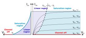
For either enhancement- or depletion-mode devices, at drain-to-source voltages much less than gate-to-source voltages, changing the gate voltage will alter the channel resistance, and drain current will be proportional to drain voltage (referenced to source voltage). In this mode the FET operates like a variable resistor and the FET is said to be operating in a linear mode or ohmic mode.
If drain-to-source voltage is increased, this creates a significant asymmetrical change in the shape of the channel due to a gradient of voltage potential from source to drain. The shape of the inversion region becomes "pinched-off" near the drain end of the channel. If drain-to-source voltage is increased further, the pinch-off point of the channel begins to move away from the drain towards the source. The FET is said to be in saturation mode; some authors refer to it as active mode, for a better analogy with bipolar transistor operating regions.
The saturation mode, or the region between ohmic and saturation, is used when amplification is needed. The in-between region is sometimes considered to be part of the ohmic or linear region, even where drain current is not approximately linear with drain voltage.
Even though the conductive channel formed by gate-to-source voltage no longer connects source to drain during saturation mode, carriers are not blocked from flowing. Considering again an n-channel device, a depletion region
Depletion region
In semiconductor physics, the depletion region, also called depletion layer, depletion zone, junction region or the space charge region, is an insulating region within a conductive, doped semiconductor material where the mobile charge carriers have diffused away, or have been forced away by an...
exists in the p-type body, surrounding the conductive channel and drain and source regions. The electrons which comprise the channel are free to move out of the channel through the depletion region if attracted to the drain by drain-to-source voltage. The depletion region is free of carriers and has a resistance similar to silicon
Silicon
Silicon is a chemical element with the symbol Si and atomic number 14. A tetravalent metalloid, it is less reactive than its chemical analog carbon, the nonmetal directly above it in the periodic table, but more reactive than germanium, the metalloid directly below it in the table...
. Any increase of the drain-to-source voltage will increase the distance from drain to the pinch-off point, increasing resistance due to the depletion region proportionally to the applied drain-to-source voltage. This proportional change causes the drain-to-source current to remain relatively fixed independent of changes to the drain-to-source voltage and quite unlike the linear mode operation. Thus in saturation mode, the FET behaves as a constant-current source
Current source
A current source is an electrical or electronic device that delivers or absorbs electric current. A current source is the dual of a voltage source. The term constant-current sink is sometimes used for sources fed from a negative voltage supply...
rather than as a resistor and can be used most effectively as a voltage amplifier. In this case, the gate-to-source voltage determines the level of constant current through the channel.
Composition
The FET can be constructed from a number of semiconductors, siliconSilicon
Silicon is a chemical element with the symbol Si and atomic number 14. A tetravalent metalloid, it is less reactive than its chemical analog carbon, the nonmetal directly above it in the periodic table, but more reactive than germanium, the metalloid directly below it in the table...
being by far the most common. Most FETs are made with conventional bulk semiconductor processing techniques
Semiconductor fabrication
Semiconductor device fabrication is the process used to create the integrated circuits that are present in everyday electrical and electronic devices. It is a multiple-step sequence of photolithographic and chemical processing steps during which electronic circuits are gradually created on a wafer...
, using the single crystal semiconductor
Monocrystalline silicon
Monocrystalline silicon or single-crystal Si, or mono-Si is the base material of the electronic industry. It consists of silicon in which the crystal lattice of the entire solid is continuous, unbroken to its edges. It can be prepared intrinsic, i.e...
wafer
Wafer (electronics)
A wafer is a thin slice of semiconductor material, such as a silicon crystal, used in the fabrication of integrated circuits and other microdevices...
as the active region, or channel.
Among the more unusual body materials are amorphous silicon
Amorphous silicon
Amorphous silicon is the non-crystalline allotropic form of silicon. It can be deposited in thin films at low temperatures onto a variety of substrates, offering some unique capabilities for a variety of electronics.-Description:...
, polycrystalline silicon
Polycrystalline silicon
Polycrystalline silicon, also called polysilicon, is a material consisting of small silicon crystals. It differs from single-crystal silicon, used for electronics and solar cells, and from amorphous silicon, used for thin film devices and solar cells....
or other amorphous semiconductors in thin-film transistor
Thin-film transistor
A thin-film transistor is a special kind of field-effect transistor made by depositing thin films of a semiconductor active layer as well as the dielectric layer and metallic contacts over a supporting substrate. A common substrate is glass, since the primary application of TFTs is in liquid...
s or organic field effect transistors
OFET
An organic field-effect transistor is a field effect transistor using an organic semiconductor in its channel. OFETs can be prepared either by vacuum evaporation of small molecules, by solution-casting of polymers or small molecules, or by mechanical transfer of a peeled single-crystalline organic...
that are based on organic semiconductor
Organic semiconductor
An organic semiconductor is an organic material with semiconductor properties. Single molecules, short chain and organic polymers can be semiconductive. Semiconducting small molecules include the polycyclic aromatic compounds pentacene, anthracene, and rubrene...
s and often apply organic gate insulators
and electrode.
The FETs are manufactured using variety of materials as silicon carbide(Sic),gallium arsenide(GaAs),gallium nitride(GaN),indium gallium arsenide(InGaAs).
In June of 2011, IBM announced that it had successfully used graphene
Graphene
Graphene is an allotrope of carbon, whose structure is one-atom-thick planar sheets of sp2-bonded carbon atoms that are densely packed in a honeycomb crystal lattice. The term graphene was coined as a combination of graphite and the suffix -ene by Hanns-Peter Boehm, who described single-layer...
-based FETs in an integrated circuit
Integrated circuit
An integrated circuit or monolithic integrated circuit is an electronic circuit manufactured by the patterned diffusion of trace elements into the surface of a thin substrate of semiconductor material...
. These transistors are capable of a 100 GHz cutoff frequency, much higher than standard silicon FETs .
Types of field-effect transistors
Doping (semiconductor)
In semiconductor production, doping intentionally introduces impurities into an extremely pure semiconductor for the purpose of modulating its electrical properties. The impurities are dependent upon the type of semiconductor. Lightly and moderately doped semiconductors are referred to as extrinsic...
to produce either an N-type semiconductor
N-type semiconductor
N-type semiconductors are a type of extrinsic semiconductor where the dopant atoms are capable of providing extra conduction electrons to the host material . This creates an excess of negative electron charge carriers....
or a P-type semiconductor
P-type semiconductor
A P-type semiconductor is obtained by carrying out a process of doping: that is, adding a certain type of atoms to the semiconductor in order to increase the number of free charge carriers ....
. The drain and source may be doped of opposite type to the channel, in the case of depletion mode FETs, or doped of similar type to the channel as in enhancement mode FETs. Field-effect transistors are also distinguished by the method of insulation between channel and gate. Types of FETs are:
- CNTFETCarbon nanotube field-effect transistorA carbon nanotube field-effect transistor refers to a field-effect transistor that utilizes a single carbon nanotube or an array of carbon nanotubes as the channel material instead of bulk silicon in the traditional MOSFET structure...
(Carbon nanotube field-effect transistor) - The DEPFET is a FET formed in a fully depleted substrate and acts as a sensor, amplifier and memory node at the same time. It can be used as an image (photon) sensor.
- The DGMOSFET is a MOSFET with dual gates.
- The DNAFET is a specialized FET that acts as a biosensorBiosensorA biosensor is an analytical device for the detection of an analyte that combines a biological component with a physicochemical detector component.It consists of 3 parts:* the sensitive biological element A biosensor is an analytical device for the detection of an analyte that combines a biological...
, by using a gate made of single-strand DNA molecules to detect matching DNA strands. - The FREDFETFREDFETA FREDFET is a fast-reverse or fast-recovery epitaxial diode field-effect transistor. This specialised field-effect transistor is designed to provide a very fast recovery of the body diode, making it convenient for driving inductive loads such as electric motors, especially medium-powered...
(Fast Reverse or Fast Recovery Epitaxial Diode FET) is a specialized FET designed to provide a very fast recovery (turn-off) of the body diode. - The HEMT (high electron mobility transistor), also called a HFET (heterostructure FET), can be made using bandgap engineering in a ternary semiconductor such as AlGaAs. The fully depleted wide-band-gap material forms the isolation between gate and body.
- The IGBT (insulated-gate bipolar transistor) is a device for power control. It has a structure akin to a MOSFET coupled with a bipolar-like main conduction channel. These are commonly used for the 200-3000 V drain-to-source voltage range of operation. Power MOSFETPower MOSFETA Power MOSFET is a specific type of metal oxide semiconductor field-effect transistor designed to handle significant power levels. Compared to the other power semiconductor devices , its main advantages are high commutation speed and good efficiency at low voltages...
s are still the device of choice for drain-to-source voltages of 1 to 200 V. - The ISFETISFETISFET pH electrode also redirects here.An ISFET is an ion-sensitive field-effect transistor used for measuring ion concentrations in solution; when the ion concentration changes, the current through the transistor will change accordingly. Here, the solution is used as the gate electrode...
(ion-sensitive field-effect transistor) used to measure ion concentrations in a solution; when the ion concentration (such as H+, see pH electrode) changes, the current through the transistor will change accordingly. - The JFETJFETThe junction gate field-effect transistor is the simplest type of field-effect transistor. It can be used as an electronically-controlled switch or as a voltage-controlled resistance. Electric charge flows through a semiconducting channel between "source" and "drain" terminals...
(junction field-effect transistor) uses a reverse biased p-n junction to separate the gate from the body. - The MESFETMESFETMESFET stands for metal semiconductor field effect transistor. It is quite similar to a JFET in construction and terminology. The difference is that instead of using a p-n junction for a gate, a Schottky junction is used...
(Metal–Semiconductor Field-Effect Transistor) substitutes the p-n junctionP-n junctionA p–n junction is formed at the boundary between a P-type and N-type semiconductor created in a single crystal of semiconductor by doping, for example by ion implantation, diffusion of dopants, or by epitaxy .If two separate pieces of material were used, this would...
of the JFET with a Schottky barrierSchottky barrierA Schottky barrier, named after Walter H. Schottky, is a potential barrier formed at a metal–semiconductor junction which has rectifying characteristics, suitable for use as a diode...
; used in GaAs and other III-V semiconductor materials. - The MODFETMODFETThe modulated-doping field effect transistor or modulation-doped field effect transistor is a type of a field-effect transistor, also known as the High Electron Mobility Transistor . Like other FETs, MODFETs are used in integrated circuits as digital on-off switches...
(Modulation-Doped Field Effect Transistor) uses a quantum wellQuantum wellA quantum well is a potential well with only discrete energy values.One technology to create quantization is to confine particles, which were originally free to move in three dimensions, to two dimensions, forcing them to occupy a planar region...
structure formed by graded doping of the active region. - The MOSFETMOSFETThe metal–oxide–semiconductor field-effect transistor is a transistor used for amplifying or switching electronic signals. The basic principle of this kind of transistor was first patented by Julius Edgar Lilienfeld in 1925...
(Metal–Oxide–Semiconductor Field-Effect Transistor) utilizes an insulatorElectrical insulationthumb|250px|[[Coaxial Cable]] with dielectric insulator supporting a central coreThis article refers to electrical insulation. For insulation of heat, see Thermal insulation...
(typically SiO2Silicon dioxideThe chemical compound silicon dioxide, also known as silica , is an oxide of silicon with the chemical formula '. It has been known for its hardness since antiquity...
) between the gate and the body. - The NOMFETNOMFETNOMFET is a nanoparticle organic memory field-effect transistor. The transistor is designed to mimic the feature of the human synapse known as plasticity, or the variation of the speed and strength of the signal going from neuron to neuron. The transistor uses gold nano-particles of about 5—20 nm...
is a Nanoparticle Organic Memory Field-Effect Transistor.http://www.sciencedaily.com/releases/2010/01/100125122101.htm - The OFETOFETAn organic field-effect transistor is a field effect transistor using an organic semiconductor in its channel. OFETs can be prepared either by vacuum evaporation of small molecules, by solution-casting of polymers or small molecules, or by mechanical transfer of a peeled single-crystalline organic...
is an Organic Field-Effect Transistor using an organic semiconductor in its channel. - The GNRFET is a Field-Effect Transistor that uses a graphene nanoribbonGraphene nanoribbonsGraphene nanoribbons , often abbreviated GNRs, are thin strips of graphene or unrolled single-walled carbon nanotubes...
for its channel. - The VeSFET (Vertical-Slit Field-Effect Transistor) is a square-shaped junction-less FET with a narrow slit connecting the source and drain at opposite corners. Two gates occupy the other corners, and control the current through the slit. http://vestics.org/twiki/bin/view/Main/WebHome http://www.ece.cmu.edu/~cssi/research/manufacturing.html
Advantages of FET
The main advantage of the FET is its high input resistance, on the order of 100M ohms or more. Thus, it is a voltage-controlled device, and shows a high degree of isolation between input and output. It is a unipolar device, depending only upon majority current flow. It is less noisy and is thus found in FM tuners for quiet reception. It is relatively immune to radiation. It exhibits no offset voltage at zero drain current and hence makes an excellent signal chopper. It typically has better thermal stability than a BJT.Disadvantages of FET
It has relatively low gain-bandwidth product compared to a BJT. The MOSFET has a drawback of being very susceptible to overload voltages, thus requiring special handling during installation.Uses
IGBTs see application in switching internal combustion engine ignition coils, where fast switching and voltage blocking capabilities are important.The most commonly used FET is the MOSFET
MOSFET
The metal–oxide–semiconductor field-effect transistor is a transistor used for amplifying or switching electronic signals. The basic principle of this kind of transistor was first patented by Julius Edgar Lilienfeld in 1925...
. The CMOS
CMOS
Complementary metal–oxide–semiconductor is a technology for constructing integrated circuits. CMOS technology is used in microprocessors, microcontrollers, static RAM, and other digital logic circuits...
(complementary metal oxide semiconductor) process technology is the basis for modern digital
Digital
A digital system is a data technology that uses discrete values. By contrast, non-digital systems use a continuous range of values to represent information...
integrated circuit
Integrated circuit
An integrated circuit or monolithic integrated circuit is an electronic circuit manufactured by the patterned diffusion of trace elements into the surface of a thin substrate of semiconductor material...
s. This process technology uses an arrangement where the (usually "enhancement-mode") p-channel MOSFET and n-channel MOSFET are connected in series such that when one is on, the other is off.
The fragile insulating layer of the MOSFET between the gate and channel makes it vulnerable to electrostatic damage
Electrostatic discharge
Electrostatic discharge is a serious issue in solid state electronics, such as integrated circuits. Integrated circuits are made from semiconductor materials such as silicon and insulating materials such as silicon dioxide...
during handling. This is not usually a problem after the device has been installed in a properly designed circuit.
In FETs electrons can flow in either direction through the channel when operated in the linear mode, and the naming convention of drain terminal and source terminal is somewhat arbitrary, as the devices are typically (but not always) built symmetrically from source to drain. This makes FETs suitable for switching analog signals between paths (multiplexing
Multiplexing
The multiplexed signal is transmitted over a communication channel, which may be a physical transmission medium. The multiplexing divides the capacity of the low-level communication channel into several higher-level logical channels, one for each message signal or data stream to be transferred...
). With this concept, one can construct a solid-state mixing board, for example.
A common use of the FET is as an amplifier. For example, due to its large input resistance and low output resistance, it is effective as a buffer in common-drain (source follower) configuration.
External links
- PBS The Field Effect Transistor
- Junction Field Effect Transistor
- The Enhancement Mode MOSFET
- CMOS gate circuitry
- Winning the Battle Against Latchup in CMOS Analog Switches
- Nanotube FETs at IBM Research
- Field Effect Transistors in Theory and Practice
- The Field Effect Transistor as a Voltage Controlled Resistor