

Scanning electron microscope
Encyclopedia
Electron microscope
An electron microscope is a type of microscope that uses a beam of electrons to illuminate the specimen and produce a magnified image. Electron microscopes have a greater resolving power than a light-powered optical microscope, because electrons have wavelengths about 100,000 times shorter than...
that images a sample by scanning it with a high-energy beam of electron
Electron
The electron is a subatomic particle with a negative elementary electric charge. It has no known components or substructure; in other words, it is generally thought to be an elementary particle. An electron has a mass that is approximately 1/1836 that of the proton...
s in a raster scan
Raster scan
A raster scan, or raster scanning, is the rectangular pattern of image capture and reconstruction in television. By analogy, the term is used for raster graphics, the pattern of image storage and transmission used in most computer bitmap image systems...
pattern. The electrons interact with the atoms that make up the sample producing signals that contain information about the sample's surface topography
Topography
Topography is the study of Earth's surface shape and features or those ofplanets, moons, and asteroids...
, composition, and other properties such as electrical conductivity.
The types of signals produced by an SEM include secondary electrons
Secondary electrons
Secondary electrons are electrons generated as ionization products. They are called 'secondary' because they are generated by other radiation . This radiation can be in the form of ions, electrons, or photons with sufficiently high energy, i.e. exceeding the ionization potential...
, back-scattered
Backscatter
In physics, backscatter is the reflection of waves, particles, or signals back to the direction they came from. It is a diffuse reflection due to scattering, as opposed to specular reflection like a mirror...
electrons (BSE), characteristic X-rays
Energy-dispersive X-ray spectroscopy
Energy-dispersive X-ray spectroscopy is an analytical technique used for the elemental analysis or chemical characterization of a sample. It relies on the investigation of an interaction of a some source of X-ray excitation and a sample...
, light (cathodoluminescence
Cathodoluminescence
Cathodoluminescence is an optical and electrical phenomenon whereby a beam of electrons is generated by an electron gun and then impacts on a luminescent material such as a phosphor, causing the material to emit visible light. The most common example is the screen of a television...
), specimen current and transmitted electrons. Secondary electron detectors are common in all SEMs, but it is rare that a single machine would have detectors for all possible signals. The signals result from interactions of the electron beam with atoms at or near the surface of the sample. In the most common or standard detection mode, secondary electron imaging or SEI, the SEM can produce very high-resolution images of a sample surface, revealing details less than 1 nm
Nanometre
A nanometre is a unit of length in the metric system, equal to one billionth of a metre. The name combines the SI prefix nano- with the parent unit name metre .The nanometre is often used to express dimensions on the atomic scale: the diameter...
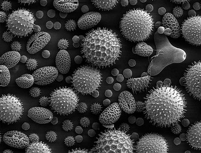
in size. Due to the very narrow electron beam, SEM micrographs have a large depth of field
Depth of field
In optics, particularly as it relates to film and photography, depth of field is the distance between the nearest and farthest objects in a scene that appear acceptably sharp in an image...
yielding a characteristic three-dimensional appearance useful for understanding the surface structure of a sample. This is exemplified by the micrograph of pollen shown to the right. A wide range of magnifications is possible, from about 10 times (about equivalent to that of a powerful hand-lens) to more than 500,000 times, about 250 times the magnification limit of the best light microscopes. Back-scattered electrons (BSE) are beam electrons that are reflected from the sample by elastic scattering
Elastic scattering
In scattering theory and in particular in particle physics, elastic scattering is one of the specific forms of scattering. In this process, the kinetic energy of the incident particles is conserved, only their direction of propagation is modified .-Electron elastic scattering:When an alpha particle...
. BSE are often used in analytical SEM along with the spectra made from the characteristic X-rays. Because the intensity of the BSE signal is strongly related to the atomic number (Z) of the specimen, BSE images can provide information about the distribution of different elements in the sample. For the same reason, BSE imaging can image colloidal gold
Colloidal gold
Colloidal gold is a suspension of sub-micrometre-sized particles of gold in a fluid — usually water. The liquid is usually either an intense red colour , or a dirty yellowish colour ....
immuno-labels
Immunogold labelling
Immunogold labelling or Immunogold staining is a staining technique used in electron microscopy. Colloidal gold particles are most often attached to secondary antibodies which are in turn attached to primary antibodies designed to bind a specific protein or other cell component...
of 5 or 10 nm diameter, which would otherwise be difficult or impossible to detect in secondary electron images in biological specimens. Characteristic X-ray
X-ray
X-radiation is a form of electromagnetic radiation. X-rays have a wavelength in the range of 0.01 to 10 nanometers, corresponding to frequencies in the range 30 petahertz to 30 exahertz and energies in the range 120 eV to 120 keV. They are shorter in wavelength than UV rays and longer than gamma...
s are emitted when the electron beam removes an inner shell electron
Electron shell
An electron shell may be thought of as an orbit followed by electrons around an atom's nucleus. The closest shell to the nucleus is called the "1 shell" , followed by the "2 shell" , then the "3 shell" , and so on further and further from the nucleus. The shell letters K,L,M,.....
from the sample, causing a higher energy electron
Energy level
A quantum mechanical system or particle that is bound -- that is, confined spatially—can only take on certain discrete values of energy. This contrasts with classical particles, which can have any energy. These discrete values are called energy levels...
to fill the shell and release energy. These characteristic X-rays are used to identify the composition and measure the abundance of elements in the sample.
History
The first SEM image was obtained by Max KnollMax Knoll
Max Knoll was a German electrical engineer.Knoll was born in Wiesbaden and studied in Munich and at the Technical University of Berlin, where he obtained his doctorate in the Institute for High Voltage Technology...
, who in 1935 obtained an image of silicon steel
Electrical steel
Electrical steel, also called lamination steel, silicon electrical steel, silicon steel, relay steel or transformer steel, is specialty steel tailored to produce certain magnetic properties, such as a small hysteresis area and high permeability.The material is usually manufactured in the form of...
showing electron channeling contrast. Further pioneering work on the physical principles of the SEM and beam specimen interactions was performed by Manfred von Ardenne
Manfred von Ardenne
Manfred von Ardenne was a German research and applied physicist and inventor. He took out approximately 600 patents in fields including electron microscopy, medical technology, nuclear technology, plasma physics, and radio and television technology...
in 1937, who produced a British patent but never made a practical instrument. The SEM was further developed by Professor Sir Charles Oatley
Charles Oatley
Sir Charles William Oatley OBE, FRS FREng was Professor of Electrical Engineering, University of Cambridge, 1960–1971, and developer of one of the first commercial scanning electron microscopes....
and his postgraduate student Gary Stewart and was first marketed in 1965 by the Cambridge Scientific Instrument Company
Cambridge Scientific Instrument Company
Cambridge Scientific Instrument Company was a company founded in 1881 by Horace Darwin and Albert George Dew-Smith to manufacture scientific instruments....
as the "Stereoscan". The first instrument was delivered to DuPont.
Scanning process and image formation
In a typical SEM, an electron beam is thermionically emitted from an electron gunElectron gun
An electron gun is an electrical component that produces an electron beam that has a precise kinetic energy and is most often used in television sets and computer displays which use cathode ray tube technology, as well as in other instruments, such as electron microscopes and particle...
fitted with a tungsten
Tungsten
Tungsten , also known as wolfram , is a chemical element with the chemical symbol W and atomic number 74.A hard, rare metal under standard conditions when uncombined, tungsten is found naturally on Earth only in chemical compounds. It was identified as a new element in 1781, and first isolated as...
filament cathode
Cathode
A cathode is an electrode through which electric current flows out of a polarized electrical device. Mnemonic: CCD .Cathode polarity is not always negative...
. Tungsten is normally used in thermionic electron guns because it has the highest melting point and lowest vapour pressure of all metals, thereby allowing it to be heated for electron emission, and because of its low cost. Other types of electron emitters include lanthanum hexaboride
Lanthanum hexaboride
]]Lanthanum hexaboride is an inorganic chemical, a boride of lanthanum. It is a refractory ceramic material that has a melting point of 2210 °C, and is insoluble in water and hydrochloric acid. It has a low work function and one of the highest electron emissivities known, and is stable in...
cathodes, which can be used in a standard tungsten filament SEM if the vacuum system is upgraded and field emission gun
Field emission gun
A field emission gun is a type of electron gun in which a sharply-pointed Müller-type emitter is held at several kilovolts negative potential relative to a nearby electrode, so that there is sufficient potential gradient at the emitter surface to cause field electron emission...
s (FEG), which may be of the cold-cathode type using tungsten single crystal emitters or the thermally assisted Schottky
Walter H. Schottky
Walter Hermann Schottky was a German physicist who played a major early role in developing the theory of electron and ion emission phenomena, invented the screen-grid vacuum tube in 1915 and the pentode in 1919 while working at Siemens, and later made many significant contributions in the areas of...
type, using emitters of zirconium oxide.
The electron beam, which typically has an energy
Energy
In physics, energy is an indirectly observed quantity. It is often understood as the ability a physical system has to do work on other physical systems...
ranging from 0.2 keV
Electronvolt
In physics, the electron volt is a unit of energy equal to approximately joule . By definition, it is equal to the amount of kinetic energy gained by a single unbound electron when it accelerates through an electric potential difference of one volt...
to 40 keV, is focused by one or two condenser lenses to a spot about 0.4 nm to 5 nm in diameter. The beam passes through pairs of scanning coils or pairs of deflector plates in the electron column, typically in the final lens, which deflect the beam in the x and y axes so that it scans in a raster
Raster scan
A raster scan, or raster scanning, is the rectangular pattern of image capture and reconstruction in television. By analogy, the term is used for raster graphics, the pattern of image storage and transmission used in most computer bitmap image systems...
fashion over a rectangular area of the sample surface.
When the primary electron beam interacts with the sample, the electrons lose energy by repeated random scattering and absorption within a teardrop-shaped volume of the specimen known as the interaction volume, which extends from less than 100 nm to around 5 µm into the surface. The size of the interaction volume depends on the electron's landing energy, the atomic number of the specimen and the specimen's density. The energy exchange between the electron beam and the sample results in the reflection of high-energy electrons by elastic scattering
Elastic scattering
In scattering theory and in particular in particle physics, elastic scattering is one of the specific forms of scattering. In this process, the kinetic energy of the incident particles is conserved, only their direction of propagation is modified .-Electron elastic scattering:When an alpha particle...
, emission of secondary electrons by inelastic scattering
Inelastic scattering
In particle physics and chemistry, inelastic scattering is a fundamental scattering process in which the kinetic energy of an incident particle is not conserved . In an inelastic scattering process, some of the energy of the incident particle is lost or gained...
and the emission of electromagnetic radiation
Electromagnetic radiation
Electromagnetic radiation is a form of energy that exhibits wave-like behavior as it travels through space...
, each of which can be detected by specialized detectors. The beam current absorbed by the specimen can also be detected and used to create images of the distribution of specimen current. Electronic amplifiers
Electronics
Electronics is the branch of science, engineering and technology that deals with electrical circuits involving active electrical components such as vacuum tubes, transistors, diodes and integrated circuits, and associated passive interconnection technologies...
of various types are used to amplify the signals, which are displayed as variations in brightness on a cathode ray tube
Cathode ray tube
The cathode ray tube is a vacuum tube containing an electron gun and a fluorescent screen used to view images. It has a means to accelerate and deflect the electron beam onto the fluorescent screen to create the images. The image may represent electrical waveforms , pictures , radar targets and...
. The raster scanning of the CRT display is synchronised with that of the beam on the specimen in the microscope, and the resulting image is therefore a distribution map of the intensity of the signal being emitted from the scanned area of the specimen. The image may be captured by photograph
Photograph
A photograph is an image created by light falling on a light-sensitive surface, usually photographic film or an electronic imager such as a CCD or a CMOS chip. Most photographs are created using a camera, which uses a lens to focus the scene's visible wavelengths of light into a reproduction of...
y from a high-resolution cathode ray tube, but in modern machines is digitally captured and displayed on a computer monitor and saved to a computer's hard disk.
Magnification
MagnificationMagnification
Magnification is the process of enlarging something only in appearance, not in physical size. This enlargement is quantified by a calculated number also called "magnification"...
in a SEM can be controlled over a range of up to 6 orders of magnitude
Order of magnitude
An order of magnitude is the class of scale or magnitude of any amount, where each class contains values of a fixed ratio to the class preceding it. In its most common usage, the amount being scaled is 10 and the scale is the exponent being applied to this amount...
from about 10 to 500,000 times. Unlike optical and transmission electron microscopes, image magnification in the SEM is not a function of the power of the objective lens
Objective (optics)
In an optical instrument, the objective is the optical element that gathers light from the object being observed and focuses the light rays to produce a real image. Objectives can be single lenses or mirrors, or combinations of several optical elements. They are used in microscopes, telescopes,...
. SEMs may have condenser and objective lenses, but their function is to focus the beam to a spot, and not to image the specimen. Provided the electron gun
Electron gun
An electron gun is an electrical component that produces an electron beam that has a precise kinetic energy and is most often used in television sets and computer displays which use cathode ray tube technology, as well as in other instruments, such as electron microscopes and particle...
can generate a beam with sufficiently small diameter, a SEM could in principle work entirely without condenser or objective lenses, although it might not be very versatile or achieve very high resolution. In a SEM, as in scanning probe microscopy
Scanning probe microscopy
Scanning Probe Microscopy is a branch of microscopy that forms images of surfaces using a physical probe that scans the specimen. An image of the surface is obtained by mechanically moving the probe in a raster scan of the specimen, line by line, and recording the probe-surface interaction as a...
, magnification results from the ratio of the dimensions of the raster on the specimen and the raster on the display device. Assuming that the display screen has a fixed size, higher magnification results from reducing the size of the raster on the specimen, and vice versa. Magnification is therefore controlled by the current supplied to the x, y scanning coils, or the voltage supplied to the x, y deflector plates, and not by objective lens power.
Sample preparation
All samples must also be of an appropriate size to fit in the specimen chamber and are generally mounted rigidly on a specimen holder called a specimen stub. Several models of SEM can examine any part of a 6 inches (15.2 cm) semiconductor wafer, and some can tilt an object of that size to 45°.For conventional imaging in the SEM, specimens must be electrically conductive, at least at the surface, and electrically grounded
Ground (electricity)
In electrical engineering, ground or earth may be the reference point in an electrical circuit from which other voltages are measured, or a common return path for electric current, or a direct physical connection to the Earth....
to prevent the accumulation of electrostatic charge
Static electricity
Static electricity refers to the build-up of electric charge on the surface of objects. The static charges remain on an object until they either bleed off to ground or are quickly neutralized by a discharge. Static electricity can be contrasted with current electricity, which can be delivered...
at the surface. Metal objects require little special preparation for SEM except for cleaning and mounting on a specimen stub. Nonconductive specimens tend to charge when scanned by the electron beam, and especially in secondary electron imaging mode, this causes scanning faults and other image artifacts. They are therefore usually coated with an ultrathin coating of electrically conducting material, deposited on the sample either by low-vacuum sputter coating
Sputter coating
Sputter coating in scanning electron microscopy is a process of covering a specimen with a very thin layer of conducting material, typically a metal, such as a gold/palladium alloy. Conductive coating is needed to prevent charging of a specimen with an electron beam in conventional SEM mode...
or by high-vacuum evaporation. Conductive materials in current use for specimen coating include gold
Gold
Gold is a chemical element with the symbol Au and an atomic number of 79. Gold is a dense, soft, shiny, malleable and ductile metal. Pure gold has a bright yellow color and luster traditionally considered attractive, which it maintains without oxidizing in air or water. Chemically, gold is a...
, gold/palladium
Palladium
Palladium is a chemical element with the chemical symbol Pd and an atomic number of 46. It is a rare and lustrous silvery-white metal discovered in 1803 by William Hyde Wollaston. He named it after the asteroid Pallas, which was itself named after the epithet of the Greek goddess Athena, acquired...
alloy, platinum
Platinum
Platinum is a chemical element with the chemical symbol Pt and an atomic number of 78. Its name is derived from the Spanish term platina del Pinto, which is literally translated into "little silver of the Pinto River." It is a dense, malleable, ductile, precious, gray-white transition metal...
, osmium
Osmium
Osmium is a chemical element with the symbol Os and atomic number 76. Osmium is a hard, brittle, blue-gray or blue-blacktransition metal in the platinum family, and is the densest natural element. Osmium is twice as dense as lead. The density of osmium is , slightly greater than that of iridium,...
, iridium
Iridium
Iridium is the chemical element with atomic number 77, and is represented by the symbol Ir. A very hard, brittle, silvery-white transition metal of the platinum family, iridium is the second-densest element and is the most corrosion-resistant metal, even at temperatures as high as 2000 °C...
, tungsten
Tungsten
Tungsten , also known as wolfram , is a chemical element with the chemical symbol W and atomic number 74.A hard, rare metal under standard conditions when uncombined, tungsten is found naturally on Earth only in chemical compounds. It was identified as a new element in 1781, and first isolated as...
, chromium
Chromium
Chromium is a chemical element which has the symbol Cr and atomic number 24. It is the first element in Group 6. It is a steely-gray, lustrous, hard metal that takes a high polish and has a high melting point. It is also odorless, tasteless, and malleable...
, and graphite
Graphite
The mineral graphite is one of the allotropes of carbon. It was named by Abraham Gottlob Werner in 1789 from the Ancient Greek γράφω , "to draw/write", for its use in pencils, where it is commonly called lead . Unlike diamond , graphite is an electrical conductor, a semimetal...
. Additionally, coating may increase signal/noise ratio for samples of low atomic number
Atomic number
In chemistry and physics, the atomic number is the number of protons found in the nucleus of an atom and therefore identical to the charge number of the nucleus. It is conventionally represented by the symbol Z. The atomic number uniquely identifies a chemical element...
(Z). The improvement arises because secondary electron emission for high-Z materials is enhanced.
An alternative to coating for some biological samples is to increase the bulk conductivity of the material by impregnation with osmium using variants of the OTO staining method (O-osmium, T-thiocarbohydrazide, O-osmium).
Nonconducting specimens may be imaged uncoated using specialized SEM instrumentation such as the "Environmental SEM" (ESEM) or field emission gun (FEG) SEMs operated at low voltage. Environmental SEM instruments place the specimen in a relatively high-pressure chamber where the working distance is short and the electron optical column is differentially pumped to keep vacuum adequately low at the electron gun. The high-pressure region around the sample in the ESEM neutralizes charge and provides an amplification of the secondary electron signal.
Low-voltage SEM of non-conducting specimens can be operationally difficult to accomplish in a conventional SEM and is typically a research application for specimens that are sensitive to the process of applying conductive coatings. Low-voltage SEM of non-conducting specimens can be operationally difficult to accomplish in a conventional SEM and is typically a research application for specimens that are sensitive to the process of applying conductive coatings. Low-voltage SEM is typically conducted in an FEG-SEM because the FEG is capable of producing high primary electron brightness even at low accelerating potentials. Operating conditions to prevent charging of non-conductive specimens must be adjusted such that the incoming beam current was equal to sum of outcoming secondary and backscattered electrons currents. It usually occurs at accelerating voltages of 0.5-4 kV.
Embedding in a resin
Resin
Resin in the most specific use of the term is a hydrocarbon secretion of many plants, particularly coniferous trees. Resins are valued for their chemical properties and associated uses, such as the production of varnishes, adhesives, and food glazing agents; as an important source of raw materials...
with further polishing to a mirror-like finish can be used for both biological and materials specimens when imaging in backscattered electrons or when doing quantitative X-ray microanalysis.
Biological samples
For SEM, a specimen is normally required to be completely dry, since the specimen chamber is at high vacuum. Hard, dry materials such as wood, bone, feathers, dried insects, or shells can be examined with little further treatment, but living cells and tissues and whole, soft-bodied organisms usually require chemical fixationFixation
Fixation may refer to the following:In science:*Fixation , the state in which an individual becomes obsessed with an attachment to another human, an animal, or an inanimate object...
to preserve and stabilize their structure. Fixation is usually performed by incubation in a solution of a buffered
Buffer solution
A buffer solution is an aqueous solution consisting of a mixture of a weak acid and its conjugate base or a weak base and its conjugate acid. It has the property that the pH of the solution changes very little when a small amount of strong acid or base is added to it. Buffer solutions are used as a...
chemical fixative, such as glutaraldehyde
Glutaraldehyde
Glutaraldehyde is an organic compound with the formula CH22. A pungent colorless oily liquid, glutaraldehyde is used to disinfect medical and dental equipment...
, sometimes in combination with formaldehyde
Formaldehyde
Formaldehyde is an organic compound with the formula CH2O. It is the simplest aldehyde, hence its systematic name methanal.Formaldehyde is a colorless gas with a characteristic pungent odor. It is an important precursor to many other chemical compounds, especially for polymers...
and other fixatives, and optionally followed by postfixation with osmium tetroxide. The fixed tissue is then dehydrated. Because air-drying causes collapse and shrinkage, this is commonly achieved by replacement of water
Water
Water is a chemical substance with the chemical formula H2O. A water molecule contains one oxygen and two hydrogen atoms connected by covalent bonds. Water is a liquid at ambient conditions, but it often co-exists on Earth with its solid state, ice, and gaseous state . Water also exists in a...
in the cells with organic solvents such as ethanol
Ethanol
Ethanol, also called ethyl alcohol, pure alcohol, grain alcohol, or drinking alcohol, is a volatile, flammable, colorless liquid. It is a psychoactive drug and one of the oldest recreational drugs. Best known as the type of alcohol found in alcoholic beverages, it is also used in thermometers, as a...
or acetone
Acetone
Acetone is the organic compound with the formula 2CO, a colorless, mobile, flammable liquid, the simplest example of the ketones.Acetone is miscible with water and serves as an important solvent in its own right, typically as the solvent of choice for cleaning purposes in the laboratory...
, and replacement of these solvents in turn with a transitional fluid such as liquid carbon dioxide
Carbon dioxide
Carbon dioxide is a naturally occurring chemical compound composed of two oxygen atoms covalently bonded to a single carbon atom...
by critical point drying. The carbon dioxide is finally removed while in a supercritical state, so that no gas-liquid interface is present within the sample during drying. The dry specimen is usually mounted on a specimen stub using an adhesive such as epoxy resin or electrically conductive double-sided adhesive tape, and sputter-coated
Sputter coating
Sputter coating in scanning electron microscopy is a process of covering a specimen with a very thin layer of conducting material, typically a metal, such as a gold/palladium alloy. Conductive coating is needed to prevent charging of a specimen with an electron beam in conventional SEM mode...
with gold or gold/palladium alloy before examination in the microscope.
If the SEM is equipped with a cold stage for cryo-microscopy, cryofixation
Cryofixation
Cryofixation is a technique for fixation or stabilisation of biological materials as the first step in specimen preparation for electron microscopy...
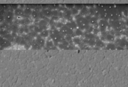
may be used and low-temperature scanning electron microscopy performed on the cryogenically fixed specimens. Cryo-fixed specimens may be cryo-fractured under vacuum in a special apparatus to reveal internal structure, sputter-coated, and transferred onto the SEM cryo-stage while still frozen. Low-temperature scanning electron microscopy is also applicable to the imaging of temperature-sensitive materials such as ice (see e.g. illustration at left) and fats.
Freeze-fracturing, freeze-etch or freeze-and-break is a preparation method particularly useful for examining lipid membranes and their incorporated proteins in "face on" view. The preparation method reveals the proteins embedded in the lipid bilayer.
Gold has a high atomic number and sputter-coating with gold produces high topographic contrast and resolution. However, the coating has a thickness of a few nanometers, and can obscure the underlying fine detail of the specimen at very high magnification. Low-vacuum SEMs with differential pumping apertures allow samples to be imaged without such coating and without the loss of natural contrast caused by the coating, but are unable to achieve the resolution attainable by conventional SEMs with coated specimens.
Materials
Back scattered electron imaging, quantitative X-ray analysis, and X-ray mapping of specimens often requires that the surfaces be ground and polished to an ultra smooth surface. Specimens that undergo WDSWavelength dispersive X-ray spectroscopy
The Wavelength dispersive X-ray spectroscopy is a method used to count the number of X-rays of a specific wavelength diffracted by a crystal. The wavelength of the impinging x-ray and the crystal's lattice spacings are related by Bragg's law and produce constructive interference if they fit the...
or EDS
Energy-dispersive X-ray spectroscopy
Energy-dispersive X-ray spectroscopy is an analytical technique used for the elemental analysis or chemical characterization of a sample. It relies on the investigation of an interaction of a some source of X-ray excitation and a sample...
analysis are often carbon coated. In general, metals are not coated prior to imaging in the SEM because they are conductive and provide their own pathway to ground.
Fractography
Fractography
Fractography is the study of fracture surfaces of materials. Fractographic methods are routinely used to determine the cause of failure in engineering structures, especially in product failure and the practice of forensic engineering or failure analysis...
is the study of fractured surfaces that can be done on a light microscope or commonly, on an SEM. The fractured surface is cut to a suitable size, cleaned of any organic residues, and mounted on a specimen holder for viewing in the SEM.
Integrated circuits may be cut with a focused ion beam
Focused ion beam
Focused ion beam, also known as FIB, is a technique used particularly in the semiconductor industry, materials science and increasingly in the biological field for site-specific analysis, deposition, and ablation of materials. An FIB setup is a scientific instrument that resembles a scanning...
(FIB) or other ion beam
Ion beam
An ion beam is a type of charged particle beam consisting of ions. Ion beams have many uses in electronics manufacturing and other industries. A variety of ion beam sources exist, some derived from the mercury vapor thrusters developed by NASA in the 1960s.-Ion beam etching or sputtering:One type...
milling instrument for viewing in the SEM. The SEM in the first case may be incorporated into the FIB.
Metals, geological specimens, and integrated circuits all may also be chemically polished for viewing in the SEM.
Special high-resolution coating techniques are required for high-magnification imaging of inorganic thin films.
ESEM
Environmental SEM allows use of hydrated specimens, omitting dehydration procedure. The accumulation of electric chargeElectric charge
Electric charge is a physical property of matter that causes it to experience a force when near other electrically charged matter. Electric charge comes in two types, called positive and negative. Two positively charged substances, or objects, experience a mutual repulsive force, as do two...
on the surfaces of non-metallic specimens can be avoided by using environmental SEM in which the specimen is placed in an internal chamber at higher pressure, rather than the vacuum in the electron optical column. Positively charged ions generated by beam interactions with the gas help to neutralize the negative charge on the specimen surface. The pressure of gas in the chamber can be controlled, and the type of gas used can be varied according to need. Coating is thus unnecessary. In ESEM mode X-ray analysis is prone to artifacts arose from electron beam scattering on gases of specimen chamber.
Detection of secondary electrons
The most common imaging mode collects low-energy (<50 eV) secondary electronsSecondary electrons
Secondary electrons are electrons generated as ionization products. They are called 'secondary' because they are generated by other radiation . This radiation can be in the form of ions, electrons, or photons with sufficiently high energy, i.e. exceeding the ionization potential...
that are ejected from the k-orbitals of the specimen atoms by inelastic scattering
Inelastic scattering
In particle physics and chemistry, inelastic scattering is a fundamental scattering process in which the kinetic energy of an incident particle is not conserved . In an inelastic scattering process, some of the energy of the incident particle is lost or gained...
interactions with beam electrons. Due to their low energy, these electrons originate within a few nanometers from the sample surface. The electrons are detected by an Everhart-Thornley detector
Everhart-Thornley detector
The Everhart-Thornley Detector is a secondary electron detector used in scanning electron microscopes . It is named after its designers, Thomas E. Everhart and Richard F. M...
, which is a type of scintillator
Scintillator
A scintillator is a special material, which exhibits scintillation—the property of luminescence when excited by ionizing radiation. Luminescent materials, when struck by an incoming particle, absorb its energy and scintillate, i.e., reemit the absorbed energy in the form of light...
-photomultiplier
Photomultiplier
Photomultiplier tubes , members of the class of vacuum tubes, and more specifically phototubes, are extremely sensitive detectors of light in the ultraviolet, visible, and near-infrared ranges of the electromagnetic spectrum...
system. The secondary electrons are first collected by attracting them towards an electrically biased grid at about +400 V, and then further accelerated towards a phosphor or scintillator positively biased to about +2,000 V. The accelerated secondary electrons are now sufficiently energetic to cause the scintillator to emit flashes of light (cathodoluminescence
Cathodoluminescence
Cathodoluminescence is an optical and electrical phenomenon whereby a beam of electrons is generated by an electron gun and then impacts on a luminescent material such as a phosphor, causing the material to emit visible light. The most common example is the screen of a television...
), which are conducted to a photomultiplier outside the SEM column via a light pipe and a window in the wall of the specimen chamber. The amplified electrical signal
Signal (electrical engineering)
In the fields of communications, signal processing, and in electrical engineering more generally, a signal is any time-varying or spatial-varying quantity....
output by the photomultiplier is displayed as a two-dimensional intensity distribution that can be viewed and photographed on an analogue video
Video
Video is the technology of electronically capturing, recording, processing, storing, transmitting, and reconstructing a sequence of still images representing scenes in motion.- History :...
display, or subjected to analog-to-digital conversion
Analog-to-digital converter
An analog-to-digital converter is a device that converts a continuous quantity to a discrete time digital representation. An ADC may also provide an isolated measurement...
and displayed and saved as a digital image
Digital image
A digital image is a numeric representation of a two-dimensional image. Depending on whether or not the image resolution is fixed, it may be of vector or raster type...
. This process relies on a raster-scanned primary beam. The brightness of the signal depends on the number of secondary electrons reaching the detector
Sensor
A sensor is a device that measures a physical quantity and converts it into a signal which can be read by an observer or by an instrument. For example, a mercury-in-glass thermometer converts the measured temperature into expansion and contraction of a liquid which can be read on a calibrated...
. If the beam enters the sample perpendicular to the surface, then the activated region is uniform about the axis of the beam and a certain number of electrons "escape" from within the sample. As the angle of incidence increases, the "escape" distance of one side of the beam will decrease, and more secondary electrons will be emitted. Thus steep surfaces and edges tend to be brighter than flat surfaces, which results in images with a well-defined, three-dimensional appearance. Using the signal of secondary electrons image resolution
Image resolution
Image resolution is an umbrella term that describes the detail an image holds. The term applies to raster digital images, film images, and other types of images. Higher resolution means more image detail....
less than 0.5 nm is possible.
Detection of backscattered electrons
Elastic scattering
In scattering theory and in particular in particle physics, elastic scattering is one of the specific forms of scattering. In this process, the kinetic energy of the incident particles is conserved, only their direction of propagation is modified .-Electron elastic scattering:When an alpha particle...
interactions with specimen atoms. Since heavy elements (high atomic number) backscatter electrons more strongly than light elements (low atomic number), and thus appear brighter in the image, BSE are used to detect contrast between areas with different chemical compositions. The Everhart-Thornley detector
Everhart-Thornley detector
The Everhart-Thornley Detector is a secondary electron detector used in scanning electron microscopes . It is named after its designers, Thomas E. Everhart and Richard F. M...
, which is normally positioned to one side of the specimen, is inefficient for the detection of backscattered electrons because few such electrons are emitted in the solid angle subtended by the detector, and because the positively biased detection grid has little ability to attract the higher energy BSE electrons. Dedicated backscattered electron detectors are positioned above the sample in a "doughnut" type arrangement, concentric with the electron beam, maximising the solid angle of collection. BSE detectors are usually either of scintillator
Scintillator
A scintillator is a special material, which exhibits scintillation—the property of luminescence when excited by ionizing radiation. Luminescent materials, when struck by an incoming particle, absorb its energy and scintillate, i.e., reemit the absorbed energy in the form of light...
or of semiconductor types. When all parts of the detector are used to collect electrons symmetrically about the beam, atomic number contrast is produced. However, strong topographic contrast is produced by collecting back-scattered electrons from one side above the specimen using an asymmetrical, directional BSE detector; the resulting contrast appears as illumination of the topography from that side. Semiconductor detectors can be made in radial segments that can be switched in or out to control the type of contrast produced and its directionality.
Backscattered electrons can also be used to form an electron backscatter diffraction
Electron backscatter diffraction
Electron backscatter diffraction , also known as backscatter Kikuchi diffraction is a microstructural-crystallographic technique used to examine the crystallographic orientation of many materials, which can be used to elucidate texture or preferred orientation of any crystalline or polycrystalline...
(EBSD) image that can be used to determine the crystallographic structure of the specimen.
Beam-injection analysis of semiconductors
The nature of the SEM's probe, energetic electrons, makes it uniquely suited to examining the optical and electronic properties of semiconductor materials. The high-energy electrons from the SEM beam will inject charge carrierCharge carrier
In physics, a charge carrier is a free particle carrying an electric charge, especially the particles that carry electric currents in electrical conductors. Examples are electrons and ions...
s into the semiconductor. Thus, beam electrons lose energy by promoting electrons from the valence band
Valence band
In solids, the valence band is the highest range of electron energies in which electrons are normally present at absolute zero temperature....
into the conduction band
Conduction band
In the solid-state physics field of semiconductors and insulators, the conduction band is the range of electron energies, higher than that of the valence band, sufficient to free an electron from binding with its individual atom and allow it to move freely within the atomic lattice of the material...
, leaving behind holes
Electron hole
An electron hole is the conceptual and mathematical opposite of an electron, useful in the study of physics, chemistry, and electrical engineering. The concept describes the lack of an electron at a position where one could exist in an atom or atomic lattice...
.
In a direct bandgap material, recombination of these electron-hole pairs will result in cathodoluminescence
Cathodoluminescence
Cathodoluminescence is an optical and electrical phenomenon whereby a beam of electrons is generated by an electron gun and then impacts on a luminescent material such as a phosphor, causing the material to emit visible light. The most common example is the screen of a television...
; if the sample contains an internal electric field, such as is present at a p-n junction
P-n junction
A p–n junction is formed at the boundary between a P-type and N-type semiconductor created in a single crystal of semiconductor by doping, for example by ion implantation, diffusion of dopants, or by epitaxy .If two separate pieces of material were used, this would...
, the SEM beam injection of carriers will cause electron beam induced current
Electron beam induced current
Electron beam induced current is a semiconductor analysis technique performed in a scanning electron microscope or scanning transmission electron microscope . It is used to identify buried junctions or defects in semiconductors, or to examine minority carrier properties...
(EBIC) to flow.
Cathodoluminescence and EBIC are referred to as "beam-injection" techniques, and are very powerful probes of the optoelectronic behavior of semiconductors, in particular for studying nanoscale features and defects.
Cathodoluminescence
CathodoluminescenceCathodoluminescence
Cathodoluminescence is an optical and electrical phenomenon whereby a beam of electrons is generated by an electron gun and then impacts on a luminescent material such as a phosphor, causing the material to emit visible light. The most common example is the screen of a television...
, the emission of light when atoms excited by high-energy electrons return to their ground state, is analogous to UV
Ultraviolet
Ultraviolet light is electromagnetic radiation with a wavelength shorter than that of visible light, but longer than X-rays, in the range 10 nm to 400 nm, and energies from 3 eV to 124 eV...
-induced fluorescence
Fluorescence
Fluorescence is the emission of light by a substance that has absorbed light or other electromagnetic radiation of a different wavelength. It is a form of luminescence. In most cases, emitted light has a longer wavelength, and therefore lower energy, than the absorbed radiation...
, and some materials such as zinc sulfide and some fluorescent dyes, exhibit both phenomena. Cathodoluminescence is most commonly experienced in everyday life as the light emission from the inner surface of the cathode ray tube
Cathode ray tube
The cathode ray tube is a vacuum tube containing an electron gun and a fluorescent screen used to view images. It has a means to accelerate and deflect the electron beam onto the fluorescent screen to create the images. The image may represent electrical waveforms , pictures , radar targets and...
in television sets and computer CRT monitors. In the SEM, CL detectors either collect all light emitted by the specimen or can analyse the wavelengths emitted by the specimen and display an emission spectrum
Spectrum
A spectrum is a condition that is not limited to a specific set of values but can vary infinitely within a continuum. The word saw its first scientific use within the field of optics to describe the rainbow of colors in visible light when separated using a prism; it has since been applied by...
or an image of the distribution of cathodoluminescence emitted by the specimen in real colour.
X-ray microanalysis
X-rays, which are also produced by the interaction of electrons with the sample, may also be detected in an SEM equipped for energy-dispersive X-ray spectroscopyEnergy-dispersive X-ray spectroscopy
Energy-dispersive X-ray spectroscopy is an analytical technique used for the elemental analysis or chemical characterization of a sample. It relies on the investigation of an interaction of a some source of X-ray excitation and a sample...
or wavelength dispersive X-ray spectroscopy
Wavelength dispersive X-ray spectroscopy
The Wavelength dispersive X-ray spectroscopy is a method used to count the number of X-rays of a specific wavelength diffracted by a crystal. The wavelength of the impinging x-ray and the crystal's lattice spacings are related by Bragg's law and produce constructive interference if they fit the...
.
Resolution of the SEM
The spatial resolution of the SEM depends on the size of the electron spot, which in turn depends on both the wavelength of the electrons and the electron-optical system that produces the scanning beam. The resolution is also limited by the size of the interaction volume, or the extent to which the material interacts with the electron beam. The spot size and the interaction volume are both large compared to the distances between atoms, so the resolution of the SEM is not high enough to image individual atoms, as is possible in the shorter wavelength (i.e. higher energy) transmission electron microscope (TEM). The SEM has compensating advantages, though, including the ability to image a comparatively large area of the specimen; the ability to image bulk materials (not just thin films or foils); and the variety of analytical modes available for measuring the composition and properties of the specimen. Depending on the instrument, the resolution can fall somewhere between less than 1 nm and 20 nm. By 2009, The world's highest SEM resolution at high-beam energies (0.4 nm at 30 kV) is obtained with the Hitachi S-5500. At low-beam energies, the best resolution (by 2009) is achieved by the Magellan XHR system from FEI CompanyFEI Company
FEI Company , founded in 1971, is an American supplier of electron microscopy tools to researchers, developers and manufacturers working on the nanoscale. Headquartered in Hillsboro, Oregon, the company employs 1,770 people worldwide....
(0.9 nm at 1 kV).
Environmental SEM
Conventional SEM requires samples to be imaged under vacuumVacuum
In everyday usage, vacuum is a volume of space that is essentially empty of matter, such that its gaseous pressure is much less than atmospheric pressure. The word comes from the Latin term for "empty". A perfect vacuum would be one with no particles in it at all, which is impossible to achieve in...
, because a gas atmosphere rapidly spreads and attenuates
Attenuation
In physics, attenuation is the gradual loss in intensity of any kind of flux through a medium. For instance, sunlight is attenuated by dark glasses, X-rays are attenuated by lead, and light and sound are attenuated by water.In electrical engineering and telecommunications, attenuation affects the...
electron beams. As a consequence, samples that produce a significant amount of vapour, e.g. wet biological samples or oil-bearing rock, must be either dried or cryogenically frozen. Processes involving phase transition
Phase transition
A phase transition is the transformation of a thermodynamic system from one phase or state of matter to another.A phase of a thermodynamic system and the states of matter have uniform physical properties....
s, such as the drying of adhesive
Adhesive
An adhesive, or glue, is a mixture in a liquid or semi-liquid state that adheres or bonds items together. Adhesives may come from either natural or synthetic sources. The types of materials that can be bonded are vast but they are especially useful for bonding thin materials...
s or melting of alloy
Alloy
An alloy is a mixture or metallic solid solution composed of two or more elements. Complete solid solution alloys give single solid phase microstructure, while partial solutions give two or more phases that may or may not be homogeneous in distribution, depending on thermal history...
s, liquid transport, chemical reactions, and solid-air-gas systems, in general cannot be observed. Some observations of living insects have been possible, however.
The first commercial development of the Environmental SEM (ESEM) in the late 1980s
allowed samples to be observed in low-pressure gaseous environments (e.g. 1-50 Torr
Torr
The torr is a non-SI unit of pressure with the ratio of 760 to 1 standard atmosphere, chosen to be roughly equal to the fluid pressure exerted by a millimetre of mercury, i.e., a pressure of 1 torr is approximately equal to 1 mmHg...
) and high relative humidity
Humidity
Humidity is a term for the amount of water vapor in the air, and can refer to any one of several measurements of humidity. Formally, humid air is not "moist air" but a mixture of water vapor and other constituents of air, and humidity is defined in terms of the water content of this mixture,...
(up to 100%). This was made possible by the development of a secondary-electron detector
capable of operating in the presence of water vapour and by the use of pressure-limiting apertures with differential pumping in the path of the electron beam to separate the vacuum region (around the gun and lenses) from the sample chamber.
The first commercial ESEMs were produced by the ElectroScan Corporation in USA in 1988. ElectroScan was taken over by Philips (who later sold their electron-optics division to FEI Company) in 1996.
ESEM is especially useful for non-metallic and biological materials because coating with carbon or gold is unnecessary. Uncoated Plastics and Elastomers can be routinely examined, as can uncoated biological samples. Coating can be difficult to reverse, may conceal small features on the surface of the sample and may reduce the value of the results obtained. X-ray analysis is difficult with a coating of a heavy metal, so carbon coatings are routinely used in conventional SEMs, but ESEM makes it possible to perform X-ray microanalysis on uncoated non-conductive specimens. ESEM may be the preferred for electron microscopy of unique samples from criminal or civil actions, where forensic analysis may need to be repeated by several different experts.
3D in SEM
3D data can be measured in the SEM with different methods such as:- photogrammetry (2 or 3 images from tilted specimen)
- photometric stereo (use of 4 images from BSE detector)
- inverse reconstruction using electron-material interactive models
Possible applications are roughness measurement, measurement of fractal dimension, corrosion measurement and height step measurement.
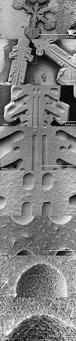
Gallery of SEM images
The following are examples of images taken using a scanning electron microscope.See also
- AFM probeAFM probeConsumable and measuring device with a sharp tip on the free swinging end of a cantilever which is protruding from a holder plate used in Atomic force microscopes . The dimensions of the cantilever are in the scale of micrometers. The radius of the tip is in the scale of a few nanometers...
- Atomic Force MicroscopeAtomic force microscopeAtomic force microscopy or scanning force microscopy is a very high-resolution type of scanning probe microscopy, with demonstrated resolution on the order of fractions of a nanometer, more than 1000 times better than the optical diffraction limit...
(AFM) - Forensic engineeringForensic engineeringForensic engineering is the investigation of materials, products, structures or components that fail or do not operate or function as intended, causing personal injury or damage to property. The consequences of failure are dealt with by the law of product liability. The field also deals with...
- Forensic science
- List of surface analysis methods
- SEM-EDX
- Transmission electron microscopyTransmission electron microscopyTransmission electron microscopy is a microscopy technique whereby a beam of electrons is transmitted through an ultra thin specimen, interacting with the specimen as it passes through...
(TEM)
External links
General- HowStuffWorks - How Scanning Electron Microscopes Work
- Notes on the SEM Notes covering all aspects of the SEM
- Scanning Electron Microscopy basics an animated tutorial on how SEM works
- Preparing a Sample for the SEM preparing a non-conducting subject for the SEM (QuickTime-movie)
History
- Microscopy History links from the University of Alabama Department of Biological Sciences
- Environmental Scanning Electron Microscope (ESEM) history
Images
- Rippel Electron Microscope Facility Many dozens of (mostly biological) SEM images from Dartmouth College.
- SEM micrographs carefully colored of daily objects, by Albert Lleal.