

Photoconductive atomic force microscopy
Encyclopedia
Photoconductive atomic force microscopy (pc-AFM) is a scientific technique..
Multi-layer photovoltaic cells have gained popularity since mid 1980s. At the time, research was primarily focused on single-layer photovoltaic
(PV) devices between two electrodes, in which PV properties rely heavily on the nature of the electrodes. In addition, single layer PV devices notoriously have a poor fill factor
. This property is largely attributed to resistance that is characteristic of the organic layer. The fundamentals of pc-AFM are modifications to traditional AFM and focus on the use of pc-AFM in PV characterization. In pc-AFM the major modifications include: a second illumination laser, an inverted microscope and a neutral density filter. These components assist in the precise alignment of the illumination laser and the AFM tip within the sample. Such modifications must complement the existing principals and instrumental modules of pc-AFM so as to minimize the effect of mechanical noise and other interferences on the cantilever and sample.
back in 1839. Becquerel noticed the generation of a photocurrent
after illumination when he submerged platinum electrodes within an aqueous solution of either silver chloride
or silver bromide
. In the early 20th century, Pochettino and Volmer studied the first organic compound, anthracene
, in which photoconductivity was observed. Anthracene was heavily studied due to its known crystal structure and its commercial availability in high-purity single anthracene crystals. The studies of photoconductive properties of organic dyes such as methylene blue
were initiated only in the early 1960s owing to the discovery of the PV effect in these dyes. In further studies, it was determined that important biological molecules such as chlorophylls, carotenes, other porphyrins as well as structurally similar phthalocyanine
s also exhibited the PV effect. Although many different blends have been researched, the market is dominated by inorganic solar cell
s which are slightly more expensive than organic based solar cells. The commonly used inorganic based solar cells include crystalline, polycrystalline
, and amorphous substrates such as silicon
, gallium selenide, gallium arsenide, copper indium gallium selenide
and cadmium telluride
.
With the high demand of cheap, clean energy sources persistently increasing, organic photovoltaic (OPV) devices (organic solar cells), have been studied extensively to help in reducing the dependence on fossil fuel and containing the emission of green house gases (especially CO2, NOx, and SOx). This global demand for solar energy increased 54% in 2010, while the United States alone has installed more than 2.3 GW of solar energy sources in 2010. Some of the attributes which make OPVs such a promising candidate to solve this problem include their low-cost of production, throughput, ruggedness, and their chemically tunable electric properties along with significant reduction in the production of greenhouse gases.
For decades, the researchers have believed that the maximum power conversion efficiency (PCE) would most likely remain below 0.1%. Only in 1979 Tang reported a two-layer, thin-film PV device, which ultimately yielded a power conversion efficiency of 1%. Tang’s research was published in 1986, which allowed others to decipher many of the problems which limited the basic understanding of the process involved in the OPVs. In later years, the majority of the research focused on the composite blend of poly(3-hexylthiopehene) (P3HT) and phenyl-C61-butyric acid methyl ester (PCBM). This, along with the research performed on fullerenes, dictated the majority of studies pertaining to OPV for many years. In more recent research, polymer-based bulk heterojunction
solar cells, along with low band-gap
donor-acceptor copolymers have been created for PCBM-based OPV devices. These low band-gap donor-acceptor copolymers are able to absorb a higher percentage of the solar spectrum as compared to other high efficiency polymers. These copolymers have been widely researched due to their ability to be tuned for specific optical and electrical properties.
To date, the best OPV devices have a maximum power conversion efficiency of approximately 8.13%. This low power conversion efficiency is directly related to discrepancies in the film morphology on the nano-scale level. Explanations of film morphology include recombination and/or trapping of charges, low open circuit voltages, heterogeneous interfaces, grain boundaries, and phase-separated domains. Many of these problems arise from the deficient knowledge of electro-optical properties on the nano-scale level. In numerous studies, it has been observed that heterogeneities in the electrical and optical properties influence device performance. These heterogeneities which occur in OPVs are a result the manufacturing process, such as annealing time, which is explained below. Research has mainly consisted of discovering exactly how this film morphology affects the device performance.
Until recently, microscopy methods used in the characterization of these OPVs consisted of atomic force microscopy (AFM), transmission electron microscopy
(TEM) and scanning transmission X-ray microscopy
(STXM). These methods are very useful in the identification of the local morphology on the film surface, but lack the ability to provide fundamental information regarding local photocurrent generation and ultimately on the device performance. To obtain information which links the electrical and optical properties, the use of electrical scanning probe microscopy
(SPM) is an active area of research. Electrostatic force microscopy (EFM) and scanning Kelvin probe microscopy
(SKPM) have been utilized in the studies of electron injection and charge trapping effects, while scanning tunneling microscopy (STM) and conductive atomic force microscopy
(c-AFM) have been used to investigate electron transport properties within these organic semiconductors.
Conductive AFM has been widely used in characterizing the local electric properties in both photovoltaic fullerene blends and organic films, but no reports have shown the use of c-AFM to display the distribution of photocurrents in organic thin films. The most recent variation of SPM devices include (tr-EFM) and photoconductive AFM (pc-AFM) . Both these techniques are capable of obtaining information regarding photo-induced charging rates with nano-scale resolution. The advantage of pc-AFM over tr-ERM is present in the maximum obtainable resolution by each method. pc-AFM can map photocurrent distributions with approximately 20 nm resolution, whereas tr-EFM was only able to obtain between 50–100 nm resolution at this time. Another important factor to note is although the tr-EFM is capable of characterizing thin films within organic solar cells, it is unable to provide the needed information regarding the capacitance gradient nor the surface potential of the thin film.
The origin of PC-AFM is due to the work performed by Gerd Binnig
and Heinrich Rohrer
on STM for which they were awarded the Nobel Prize
in physics in 1986. They fabricated an instrument called scanning tunneling microscope (STM) and demonstrated that STM provides surface topography on the atomic scale. This microscopy technique yielded resolutions which were nearly equal to scanning electron microscopy (SEM).
The working premises for all types of AFM techniques are largely dependent on the fundamentals of the AFM cantilever, metallic tip, scanning piezo-tube and the feedback loop that transfers information from lasers that guide the motion of the probe across the surface of a sample. The ultra-fine dimensions of the tip and the way the tip scans the surface produces lateral resolutions of 500 nm or less. In AFM, the cantilever and tip functions as a mass on a spring. When a force acts on the spring (cantilever), the spring response is directly related to the magnitude of the force. k is defined as the force constant of the cantilever.
Hooke's law
for cantilever motion:

The forces acting on the tip are such that the spring (cantilever) remains soft but responds to the applied force, with a detectable resonant frequency, fo. In Hooke's law, k is the spring constant of the cantilever and mo is defined as the mass acting on the cantilever: the mass of the cantilever itself and the mass of the tip. The relationship between fo and the spring constant is such that k must be very small in order to make the spring soft. Since k and mo are in a ratio, the value of mo must also decrease to increase the value of the ratio. Manipulating the values in this way provides the necessary high resonance frequency. A typical mo value has a magnitude of 10−10 kg and creates an fo of approximately 2 kHz.
Expression for resonant frequency of a spring:

Several forces affect the behavior of the cantilever
: attractive and repulsive Van der Waals forces, and electrostatic repulsion. Changes in these forces are monitored by a guide laser that is reflected off the back of the cantilever and detected by a photodetector
. Attractive forces between the atoms on the sample surface and the atom at the AFM tip draw the cantilever tip closer to the surface. When the cantilever tip and the sample surface come within a range of a few angstroms repulsive forces come into play as a result of electrostatic interactions. There is also a force exerted from the cantilever pressing down on the tip. The magnitude of the force exerted by the cantilever is dependent upon the direction of its motion, whether it is attracted or repelled from the sample surface When the tip of the cantilever and the surface come into contact, the single atom at the point of the tip and the atoms on the surface exhibit a Lennard-Jones potential
. The atoms exhibit attractive forces until a certain point and then experience repulsion from one another. The term ro is the separation at which the sum of the potentials between the two atoms is zero
Force on AFM tip in terms of Lennard-Jones potential
:

Modifications of this early work have been implemented to perform AFM analysis on both conducting and non-conducting materials. Conductive atomic force microscopy (c-AFM) is one such modification technique. The c-AFM technique operates by measuring fluctuations in current from the biased tip and sample while simultaneously measuring changes in the topographical features. In all techniques of AFM, two modes of operation can be used: contact mode and non-contact mode. In c-AFM resonant contact mode is used to obtain topographical from current that is measured between the biased AFM tip and the sample surface. In this type of operation, the current is measured in the small space between the tip and the sample surface. This quantification is based on the relationship between the current traveling through the sample and layer thickness. In the previous equation, Aeff is the effective emission area at the injecting electrode, q is the electron charge, h is planck’s constant, meff / m0 =0.5, which is the effective mass of an electron in the conduction band of a sample, d is the sample thickness and Φ is the barrier height. The symbol, β, the field enhancement factor, accounts for the non-planar, geometry of the tip used.
Relationship between conducting current and sample layer thickness:

The accuracies of all AFM techniques rely heavily on a sample scanning tube, the piezo-tube. The piezo-tube scanner is responsible for the direction of tip displacement during a sample analysis, and is dependent on the mode of analysis. The piezo components are either arranged orthogonally or manufactured as a cylinder. In all techniques, sample topography is measured by the movement of the x and y piezos. When performing non-contact mode pc-AFM, the piezo-tube keeps the probe from moving in the x and y direction and measures the photocurrent between the sample surface and conducting tip in the z-direction.
The principles of the piezo-tube is dependent upon how the piezo-electric material reacts with an applied voltage to either the interior or exterior of the tube. When voltage is applied to the two electrodes connected to the scanner, the tube will expand or contract causing motion to the AFM tip in the direction of this movement. This phenomenon is illustrated as the piezo-tube becomes displaced by an angle, θ. As the tube is displaced, the sample that, in traditional AFM is fixed to the tube generates lateral translation and rotation relative to the AFM tip, thus movement of the tip is generated in the x and y directions When voltage is applied of the inside of the tube, movement in the z-direction is implemented.
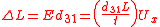
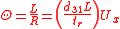
The relationship between the movement of the piezo-tube and the direction of the displacement of the AFM tip assumes that the tube is perfectly symmetric. When no voltage is applied to the tube the z-axis bisects the tube, sample and sample stage symmetrically. When a voltage is applied to the exterior of the tube (x and y motion), the expansion of the tube can be understood as a circular arc. In this equation, the r term indicates the outside radius of the piezo-tube, R is the curvature radius of the tube with applied voltage, θ is the bend angle of the tube, L is the initial length of the tube and ΔL is the extension of the tube after the voltage is applied. The change in length of the piezo-tube, ΔL, is expressed as the intensity of the electric field applied to the exterior of the tube, the voltage along the x-axis, Ux, and the thickness of the wall of the tube.
Expressions for bend geometry of piezo-tube:


Length displacement in terms of exterior electric field:
Expression for tube displacement, θ:
With the calculation of θ, the displacement of the probe in the x and z directions can be calculated as:
Expressions for probe displacement in the x- and z-directions:


Another fundamental concept of all AFM is the feedback loop. The feedback loop is particularly important in non-contact AFM techniques, particularly in pc-AFM. As previously mentioned, in non-contact mode the cantilever is stationary and the tip does not come into physical contact with the sample surface. The cantilever behaves as a spring and oscillates at its resonance frequency. Topological variance causes the spring-like oscillations of the cantilever to change amplitude and phase in order to prevent the tip from colliding with sample topographies. The non-contact feedback loop is used to control that changes in the oscillations of the cantilever.
The application of AFM on non-conducting samples (c-AFM) has in recent years evolved into the modification used for analysis of morphologies on the local scale, particularly morphologies at heterojunctions of multilayered samples. Photoconductive atomic force microscopy (pc-AFM) is particularly prevalent in the development of organic photovoltaic devices (OPV). The fundamental modification of c-AFM to pc-AFM is the addition of an illumination source and an inverted microscope that focuses the laser to a nanometer-scale point directly underneath the conductive AFM tip. The main concept of the illumination laser point is that it must be small enough to fit within the confines of ultra-thin films. These characteristics are achieved by using a monochromatic light source and a laser filter. In the OPV application, applying the illumination laser to the confines of ultra-thin films is further assisted by the recent development of the bulk heterojunction (BHJ) mixture of electron donating and accepting material in the film.
The combination of the conductive tip and illumination laser provides photocurrent images with vertical resolutions in the range of 0 to 10 pA when overlaid with the topographical data obtained. Also unique to this modification are the spectra data gathered by comparing the current between the tip and sample to a variety of parameters including: laser wavelength, applied voltage and light intensity. The pc-AFM technique was also reported to detect local surface oxidation at a vertical resolution of 80 nm.
that is positioned adjacent to the illumination source. The technical parameters of pc-AFM are identical to those of traditional AFM techniques. This section will focus on the instrumentation necessary for AFM and then detail the requirements for pc-AFM modification.
The main instrumental components to all AFM techniques are the conductive AFM cantilever and tip, the modified piezo
components and the sample substrate. The components for photoconductive modification include: the illumination source (532 nm laser), filter and inverted microscope. When modifying traditional AFM for pc application, all components must be combined such that they do not interfere with one another and so that various sources of noise and mechanical interference do not disrupt the optical components.
In traditional instrumentation, the stage is a cylindrical piezo-tube scanner that minimizes the effect of mechanical noise
. Most cylindrical piezos are between 12 and 24 mm in length and 6 and 12 mm in diameter. The exterior of the piezo-tube is coated with a thin layer of conducting metal so that this region can sustain an electric field
. The interior of the cylinder is divided into four regions (x and y regions) by non-conducting metallic strips. Electrical leads are fixed to one end and the exterior wall of the cylinder so that a current can be applied. When a voltage is applied to the exterior, the cylinder expands in x and y direction. Voltage along the interior of the tube causes cylinder expansion in the z-direction and thus movement of the tip in the z-direction. The placement of the piezo tube is dependent upon the type of AFM performed and the mode of analysis. However the z-piezo must always be fixed above the tip and cantilever to control the z-motion. This configuration is most often seen in the c-AFM and pc-AFM modifications to make room for additional instrumental components which are placed below the scanning stage. This is particularly true for pc-AFM, which must have the piezo-components arranged above the cantilever and tip so that the illumination laser can transmit through the sample.
with applied voltage]]
In some configurations, the piezo components can be arranged in a tripod design. In this type of set-up, the x, y and z components are arranged orthogonally to one another with their apex attached to a movable pivot point. Similar to the cylindrical piezo, in the tripod design the voltage is applied to the piezo corresponding to the appropriate direction of tip displacement. In this type of set-up the sample and substrate are mounted on top of the z-piezo component. When the x and y piezo components are in use, the orthogonal deign causes them to push against the base of the z-piezo, causing the z-piezo to rotate about a fixed point. Applying voltage to the z-piezo causes the tube to move up and down on its pivot point.
The other essential components of AFM instrumentation include the AFM tip module, which includes: the AFM tip, the cantilever, and the guiding laser.
When the piezo-tube is positioned above the cantilever and tip, the guiding laser
is focused through the tube and onto a mirror that rests on tip of the cantilever. The guiding laser is reflected off of the mirror and detected by a photodetector. The laser senses when the forces acting on the tip change. The reflected laser beam from this phenomenon reaches the detector. The output from this detector acts as a response to the changes in force and the cantilever adjusts the position of the tip, while keeping constant the force that acts on the tip.
The instrumentation of conductive AFM (c-AFM) has evolved with the desire to measure local electrical properties of materials with high resolutions. The essential components are: the piezo-tube, the guide laser, the conducting tip, and cantilever. Although these components are identical to traditional AFM their configuration is tailored to measuring surface currents on the local scale.
As mentioned previously, the piezo-tube can be placed either above or below the sample, depending on the application of the instrumentation. In the case of c-AFM, repulsive contact mode is the predominantly used to obtain electrical current images from the surface as the sample moves in the x and y direction. Placing the z-piezo above the cantilever allows for better control of the cantilever and tip during analysis.
The material that comprises the conductive tip and cantilever can be customized for a particular application. Metal-coated cantilevers, gold wires, all-metal cantilevers and diamond
cantilevers are used. In many cases diamond is the preferred material for cantilever and/or tip because it is an extremely hard material that does not oxidize in ambient conditions. The main difference between the instrumentation of c-AFM and STM is that in c-AFM the bias voltage can be directly applied to the nanostructure (tip and substrate). In STM, on the other hand, the applied voltage must be supported within the vacuum tunneling gap between the STM probe and surface. When the tip is in close contact with the sample surface the application of bias voltage to the tip creates a vacuum gap between the tip and the sample that enables the investigation of electron transport through nanostructures.
The main components and instrumentation of c-AFM instrumentation are identical to that required for a pc-AFM module. The only modifications are the illumination source, filter and inverted microscope objective that are located beneath the sample substrate. In fact, most pc-AFM instruments are simply modified from existing cp-AFM instrumentation. The first report of this instrumental modification came in 2008. In that paper, Lee and coworkers implemented the aforementioned modifications to examine the resolution of photocurrent imaging. Their design consisted of three main units: a conductive mirror plate, steering mirror and laser source.
The main difficulty with the previously existing c-AFM instrumentation is the inability of the technique for characterizing photonic devices. Specifically, it is difficult to measure changes in local and nano-scale electrical properties that result from the photonic effect. The optical illumination component (laser) was added to the c-AFM module in order to make such properties visible. Early in development, the main concerns regarding pc-AFM include: physical configuration, laser disturbance and laser alignment. Although many of these concerns have been resolved pc-AFM modules are still widely modified from c-AFM and traditional AFM instruments.
The first main concern deals with component configuration and whether or not there is physically enough space for modification in the cramped c-AFM module. The component configuration must be such the addition of the laser illumination component does not cause disturbance to other units. Interaction between the illumination laser and the guiding laser was also a concern. First attempts to address these two issues was to place a prism between the sample tip and the surface such that the prism would allow the illumination laser to reflect at the interface between the prism and the laser and thus be focused to a localized spot on the sample surface. However, lack of space for the prism and the production of multiple light reflections when introducing a prism required a different concept for configuration.
The module constructed by Lee et al. implemented a tilted mirror plate that was positioned underneath the sample substrate. This conductive mirror was tilted at 45° and successfully reflected the illuminating laser to a focused spot directly underneath the conductive tip. The steering mirror was employed as a means of controlling the trajectory of the laser source, with this addition the position of the reflected beam on the sample could be easily adjusted for placement underneath the AFM tip. The illumination laser source was a diode-pumped solid-state laser system that produced a wavelength of 532 nm and a spot of 1 mm in the sample.
The addition of the mirror and laser underneath the sample substrate results in a higher scanning level due to raising the sample substrate. This configuration has no affect on any other instrument component and does not affect AFM performance. This result was confirmed by identical topographical images that were taken with and without the placement of the mirror and laser. This particular set-up required the separation of the x, y and z piezo-scanners The separation of piezo-tubes accounts for the elimination of x-z cross-coupling and scanning-size errors, which is common in traditional AFM.
In addition there was no evidence of laser interferences between the guiding laser and the irradiation laser. The guiding laser, at a wavelength of 650 nm, hits the mirror on the back of the conducting cantilever from vertical trajectory and is reflected away from the cantilever towards the position sensitive photodetector
(PSPD). The illumination beam, on the other hand, travels from underneath the sample platform and is reflected into position by the reflecting mirror. The angle of the mirror plate ensures that the beam does not extend past the sample surface.
The conductive AFM tip was easily aligned over the reflected illumination beam. The laser spot in the sample was reported to be 1mm in size and can be found using the AFM recording device. A convenience of this technique is that laser alignment is only necessary for imaging in the z-direction because the photocurrents are mapped in this direction. Therefore, normal AFM/c-AFM can be implemented for analysis in the x and y directions.
The instrumental module proposed by Lee et al. produced spot sizes from the illumination laser of 1 mm in thicknesses. Recent applications have altered Lee’s design in order to decrease spot size while simultaneously increasing the intensity of this laser. Recent instrumentation has replaced the angled mirror with an inverted microscope and a neutral density filter. In this device the x and y piezo’s , illumination laser and inverted microscopy are confined underneath the sample substrate, while the z-piezo remains above the conductive cantilever. In the applications of Ginger et al. a neutral-density filter is added to increase laser attenuation and the precision of laser alignment is enhanced by the addition of the inverted microscope.
One of the most common pc-AFM setups incorporates a light source, which emits in the visible spectrum along with an indium tin oxide
(ITO) semi-conductive layer (used as the bottom cathode
). The use of a gold plated silicon AFM probe is often used as the top anode in pc-AFM studies. This electrode
which carries relatively small current within it, is able to generate nano-scale holes within the sample material to which the two electrodes are able to detect the relatively small change in conductance due to the flow from the top electrode to the bottom electrode. The combination of these elements produced laser intensities in the range of 10 to 108 W/m2 and decreased the size of the laser spot to sub-micrometer dimensions making this technique useful for the application of nm thin OPV films.
In more recent studies, pc-AFM has been employed to gather information regarding the photoactive regions from the use of quantum dots. Because if their relative ease of use, along with size-tunable excitation attributes, quantum dots have commonly been applied as sensitizers in optoelectronic devices. The authors have studied the photoresponse of sub-surface foundations such as buried indium arsenide (InAs) quantum dots through the implementation of pc-AFM. Through the use of pc-AFM, information regarding quantum dot size, as well as the dispersion of quantum dots within the device, can be recorded in a non-destructive manner. This information can then be used to display local variances in photoactivity relating to heterogeneities within the film morphology.
-coated glass as their conductive substrate. Because of high cost of ITO, however, there have been attempts to utilize other semiconducting layers, such as zinc oxide
(ZnO) and carbon nanotubes as an alternative to ITO. Although these semiconductors are relatively inexpensive, high quality ITO layers are still being used extensively for PV applications. Poly(3,4-ethylenedioxythiophene) poly(styrenesulfonate), more commonly known as PEDOT:PSS
, is a transparent, polymeric conductive layer which is usually placed between the ITO and the active OPV layer. The PEDOT:PSS is a conductive polymer is stable over various applied charges. In most studies, PEDOT:PSS is spin-coated onto the ITO-coated glass substrates directly after plasma cleaning of the ITO. Plasma cleaning, as well as halo-acid etching, have been shown to improve the surface uniformity and conductivity of the substrate. This PEDOT:PSS layer is then annealed to the ITO prior to spin-coating the OPV layer onto the substrate. Studies by Pingree et al. have shown the direct correlation between annealing time and both peak and average photocurrent generation. Once this OPV film is spin-coated onto the substrate, it is then annealed at temperatures between 70 and 170 °C, for periods up to an hour depending on the procedure as well as OPV being used.
Once the sample preparation is complete, the sample is placed onto the scanning stage of the pc-AFM module. This scanning stage is used for x-y piezo translation, completely independent of the z-direction while using a z-piezo scanner. The piezo-electric material within this scanner converts a change in the applied potential into mechanical motion which moves the samples with nanometer resolution and accuracy. There are two variations in which the z-piezo scanner functions; one is contact mode while the other is tapping mode.
Many commercial AFM cantilever tips have pre-measured resonant frequencies and force constants which are provided to the customer. As sampling proceeds, the cantilever tip’s position changes, which causes the scanning laser wavelength (650 nm) to deviate from its original position on the detector. The z-piezo scanner then recognizes this deviation and moves vertically to return the laser spot to its set position. This vertical movement by the z-piezo scanner is correlated to a change in voltage. Sampling in contact mode relies upon intermolecular forces between the tip and surface as depicted by Van der Waals force
. As the sampling begins, the tip is moved close to the sample which creates a weakly attractive force between them. Another force which is often present in contact mode is capillary force due to hydration on the sample surface. This force is due to the ability of the water to contact the tip, thus creating an undesirable attractive force. Capillary force, along with several other sources of tip contamination, are key factors in the decreased resolution observed while sampling
There are considerations which need to be taken into account when determining which mode is optimal for sampling for a given application. It has been shown that sampling in contact mode with very soft samples can damage the sample and render it useless for further studies. Sampling in non-contact mode is less destructive to the sample, but the tip is more likely to drift out of contact with the surface and thus it may not record data. Drifting of the tip is also seen due to piezo hysteresis, which causes displacement due to molecular friction and polarization effects due to the applied electric field.
It is important to note the correlation between resolution and curvature of tip radius. Early STM tips used by Binning and Rohrer were fairly large, anywhere between some hundred nm to 1 µm in radius. In more recent work, the tip radius of curvature was mentioned as 10–40 nm. By reducing the radius of curvature of the tip, it allows for the enhanced detection of deviations within the OPVs surface morphology. Tips often need to be replaced due to tip rounding, which leads to a decrease in the resolution. Tip rounding occurs due to the loss of outermost atoms present at the apex of the tip which can be a result of excessive force applied or character of the sample.
Because of the extremely small radius of the AFM tip, the illumination source is allowed to be focused tighter, thus increasing its efficiency. Typical arrangements for pc-AFM contain a low powered, 532 nm laser (2–5 mW) whose beam is reflected off mirrors located beneath the scanning stage. Through the use of a charge-coupled device
(CCD), the tip can easily be positioned directly over the laser spot. Xenon arc lamp
s have also been widely used as illumination sources, but are atypical in recent work. In a study by Coffey et al., lasers of two different wavelengths (532 nm and 405 nm) are irradiated onto the same sample area. With this work, they have shown images with identical contrast which proves that the photocurrent variations are less related to spatial absorbance variation.
Most sampling procedures often begin by obtaining the dark current
images of the sample. Dark current is referred to as the photocurrent generation created by the OPV in the absence of an illumination source. The cantilever and tip are simply rastered across the sample while topographic and current measurements are obtained. This data can then be used as a reference to determine the impact the illumination process exhibits on the OPV. Short circuit measurements are also commonly performed on the OPV devices. This consists of engaging the illumination source at open current (that is applied potential to the sample is zero). Nguyen and workers noted that a positive photocurrent reading correlated to the conduction of holes, while a negative reading correlated to the conduction of electrons. This alone allowed the authors to make predictions regarding the morphology within the cell. The current density for the forward and reverse bias can calculated as follows:
Current density equation:

where J is the current density, εo is the permittivity of a vacuum, εr is the relative permeability of the medium, µ is the mobility of the medium, V is the applied bias and L is the film thickness in nanometers. The majority of the organic materials have relative permeability values of ~3 in their amorphous and crystalline states.
The range of bias commonly applied is usually limited to between −5 V to +5 V for most studies. This can be achieved by applying a forward bias or reverse bias to the sample through the spotted gold contact. By adjusting this bias, along with the current passing through the cantilever, one can adjust the repulsive/attractive forces between the sample and the tip. When a reverse bias is applied (tip is negative relative to the sample), the tip and the sample experience attractive forces between them. This current density measurement is then combined with the topographical information previously gathered from the AFM tip and cantilever. The resulting image displays the local variations in morphology with the current density measurements superimposed onto of them.
Several methods have been employed to help reduce both mechanical and acoustic vibrations within the system. Mechanical vibrations are mainly attributed to traffic in and out of a building Other sources of mechanical vibrations have often been seen in the higher stories of a building due to reduced damping from building supports. This source of vibrational noise is easily controlled through the use of a vibration isolation table. Acoustical vibrations are far more common than mechanical vibrations. This type of vibration is a result of air movement near the instrument such as fans or human voices. Several methods have been developed to help reduce this source of vibration. An easy solution for this is separating the electronic components from the stage. The reason for this separation of components is due to the cooling fans within the electrical devices. While operating, the fans lead to a constant source of vibrational noise within the system. In most cases, other methods still need to be employed to help reduce this source of noise. For instance, the instrument can be placed within a sealed box constructed of acoustic dampening material. Smaller stages also result in less surface area for acoustic vibrations to collide with, thus reducing the noise recorded. A more in depth solution consists of removing all sharp edges on the instrument. These sharp edges can excite resonances within the piezo-electric materials which increase the acoustic noise within the system.
Multi-layer photovoltaic cells have gained popularity since mid 1980s. At the time, research was primarily focused on single-layer photovoltaic
Photovoltaic effect
The photovoltaic effect is the creation of voltage or electric current in a material upon exposure to light. Though the photovoltaic effect is directly related to the photoelectric effect, they are different processes. In the photoelectric effect, electrons are ejected from a material's surface...
(PV) devices between two electrodes, in which PV properties rely heavily on the nature of the electrodes. In addition, single layer PV devices notoriously have a poor fill factor
Fill factor
Fill factor may refer to:*Fill factor , the ratio of maximum obtainable power to the product of the open-circuit voltage and short-circuit current*In vision science, the ratio of view areas to the object visible areas....
. This property is largely attributed to resistance that is characteristic of the organic layer. The fundamentals of pc-AFM are modifications to traditional AFM and focus on the use of pc-AFM in PV characterization. In pc-AFM the major modifications include: a second illumination laser, an inverted microscope and a neutral density filter. These components assist in the precise alignment of the illumination laser and the AFM tip within the sample. Such modifications must complement the existing principals and instrumental modules of pc-AFM so as to minimize the effect of mechanical noise and other interferences on the cantilever and sample.
Background
The original exploration of the PV effect can be accredited to research published by Henri BecquerelHenri Becquerel
Antoine Henri Becquerel was a French physicist, Nobel laureate, and the discoverer of radioactivity along with Marie Curie and Pierre Curie, for which all three won the 1903 Nobel Prize in Physics.-Early life:...
back in 1839. Becquerel noticed the generation of a photocurrent
Photocurrent
Photocurrent is the current that flows through a photosensitive device, such as a photodiode, as the result of exposure to radiant power.The photocurrent may occur as a result of the photoelectric, photoemissive, or photovoltaic effect....
after illumination when he submerged platinum electrodes within an aqueous solution of either silver chloride
Silver chloride
Silver chloride is a chemical compound with the chemical formula AgCl. This white crystalline solid is well known for its low solubility in water . Upon illumination or heating, silver chloride converts to silver , which is signalled by greyish or purplish coloration to some samples...
or silver bromide
Silver bromide
Silver bromide , a soft, pale-yellow, water insoluble salt well known for its unusual sensitivity to light. This property has allowed silver halides to become the basis of modern photographic materials. AgBr is widely used in photographic films and is believed by some to have been used for making...
. In the early 20th century, Pochettino and Volmer studied the first organic compound, anthracene
Anthracene
Anthracene is a solid polycyclic aromatic hydrocarbon consisting of three fused benzene rings. It is a component of coal-tar. Anthracene is used in the production of the red dye alizarin and other dyes...
, in which photoconductivity was observed. Anthracene was heavily studied due to its known crystal structure and its commercial availability in high-purity single anthracene crystals. The studies of photoconductive properties of organic dyes such as methylene blue
Methylene blue
Methylene blue is a heterocyclic aromatic chemical compound with the molecular formula C16H18N3SCl. It has many uses in a range of different fields, such as biology and chemistry. At room temperature it appears as a solid, odorless, dark green powder, that yields a blue solution when dissolved in...
were initiated only in the early 1960s owing to the discovery of the PV effect in these dyes. In further studies, it was determined that important biological molecules such as chlorophylls, carotenes, other porphyrins as well as structurally similar phthalocyanine
Phthalocyanine
Phthalocyanine is an intensely blue-green coloured macrocyclic compound that is widely used in dyeing. Phthalocyanines form coordination complexes with most elements of the periodic table...
s also exhibited the PV effect. Although many different blends have been researched, the market is dominated by inorganic solar cell
Solar cell
A solar cell is a solid state electrical device that converts the energy of light directly into electricity by the photovoltaic effect....
s which are slightly more expensive than organic based solar cells. The commonly used inorganic based solar cells include crystalline, polycrystalline
Polycrystalline
Polycrystalline materials are solids that are composed of many crystallites of varying size and orientation. The variation in direction can be random or directed, possibly due to growth and processing conditions. Fiber texture is an example of the latter.Almost all common metals, and many ceramics...
, and amorphous substrates such as silicon
Silicon
Silicon is a chemical element with the symbol Si and atomic number 14. A tetravalent metalloid, it is less reactive than its chemical analog carbon, the nonmetal directly above it in the periodic table, but more reactive than germanium, the metalloid directly below it in the table...
, gallium selenide, gallium arsenide, copper indium gallium selenide
Copper indium gallium selenide
Copper indium gallium selenide is a I-III-VI2 semiconductor material composed of copper, indium, gallium, and selenium. The material is a solid solution of copper indium selenide and copper gallium selenide...
and cadmium telluride
Cadmium telluride
Cadmium telluride is a crystalline compound formed from cadmium and tellurium. It is used as an infrared optical window and a solar cell material. It is usually sandwiched with cadmium sulfide to form a p-n junction photovoltaic solar cell...
.
With the high demand of cheap, clean energy sources persistently increasing, organic photovoltaic (OPV) devices (organic solar cells), have been studied extensively to help in reducing the dependence on fossil fuel and containing the emission of green house gases (especially CO2, NOx, and SOx). This global demand for solar energy increased 54% in 2010, while the United States alone has installed more than 2.3 GW of solar energy sources in 2010. Some of the attributes which make OPVs such a promising candidate to solve this problem include their low-cost of production, throughput, ruggedness, and their chemically tunable electric properties along with significant reduction in the production of greenhouse gases.
For decades, the researchers have believed that the maximum power conversion efficiency (PCE) would most likely remain below 0.1%. Only in 1979 Tang reported a two-layer, thin-film PV device, which ultimately yielded a power conversion efficiency of 1%. Tang’s research was published in 1986, which allowed others to decipher many of the problems which limited the basic understanding of the process involved in the OPVs. In later years, the majority of the research focused on the composite blend of poly(3-hexylthiopehene) (P3HT) and phenyl-C61-butyric acid methyl ester (PCBM). This, along with the research performed on fullerenes, dictated the majority of studies pertaining to OPV for many years. In more recent research, polymer-based bulk heterojunction
Heterojunction
A heterojunction is the interface that occurs between two layers or regions of dissimilar crystalline semiconductors. These semiconducting materials have unequal band gaps as opposed to a homojunction...
solar cells, along with low band-gap
Band gap
In solid state physics, a band gap, also called an energy gap or bandgap, is an energy range in a solid where no electron states can exist. In graphs of the electronic band structure of solids, the band gap generally refers to the energy difference between the top of the valence band and the...
donor-acceptor copolymers have been created for PCBM-based OPV devices. These low band-gap donor-acceptor copolymers are able to absorb a higher percentage of the solar spectrum as compared to other high efficiency polymers. These copolymers have been widely researched due to their ability to be tuned for specific optical and electrical properties.
To date, the best OPV devices have a maximum power conversion efficiency of approximately 8.13%. This low power conversion efficiency is directly related to discrepancies in the film morphology on the nano-scale level. Explanations of film morphology include recombination and/or trapping of charges, low open circuit voltages, heterogeneous interfaces, grain boundaries, and phase-separated domains. Many of these problems arise from the deficient knowledge of electro-optical properties on the nano-scale level. In numerous studies, it has been observed that heterogeneities in the electrical and optical properties influence device performance. These heterogeneities which occur in OPVs are a result the manufacturing process, such as annealing time, which is explained below. Research has mainly consisted of discovering exactly how this film morphology affects the device performance.
Until recently, microscopy methods used in the characterization of these OPVs consisted of atomic force microscopy (AFM), transmission electron microscopy
Transmission electron microscopy
Transmission electron microscopy is a microscopy technique whereby a beam of electrons is transmitted through an ultra thin specimen, interacting with the specimen as it passes through...
(TEM) and scanning transmission X-ray microscopy
X-ray microscope
An X-ray microscope uses electromagnetic radiation in the soft X-ray band to produce images of very small objects.Unlike visible light, X-rays do not reflect or refract easily, and they are invisible to the human eye. Therefore the basic process of an X-ray microscope is to expose film or use a...
(STXM). These methods are very useful in the identification of the local morphology on the film surface, but lack the ability to provide fundamental information regarding local photocurrent generation and ultimately on the device performance. To obtain information which links the electrical and optical properties, the use of electrical scanning probe microscopy
Scanning probe microscopy
Scanning Probe Microscopy is a branch of microscopy that forms images of surfaces using a physical probe that scans the specimen. An image of the surface is obtained by mechanically moving the probe in a raster scan of the specimen, line by line, and recording the probe-surface interaction as a...
(SPM) is an active area of research. Electrostatic force microscopy (EFM) and scanning Kelvin probe microscopy
Kelvin probe force microscope
Kelvin probe force microscopy , also known as surface potential microscopy, is a noncontact variant of atomic force microscopy that was invented in 1991. With KPFM, the work function of surfaces can be observed at atomic or molecular scales...
(SKPM) have been utilized in the studies of electron injection and charge trapping effects, while scanning tunneling microscopy (STM) and conductive atomic force microscopy
Conductive atomic force microscopy
Conductive atomic force microscopy is a variation of atomic force microscopy and scanning tunneling microscopy , which uses electrical current to construct the surface profile of the studied sample. The current is flowing through the metal-coated tip of the microscope and the conducting sample...
(c-AFM) have been used to investigate electron transport properties within these organic semiconductors.
Conductive AFM has been widely used in characterizing the local electric properties in both photovoltaic fullerene blends and organic films, but no reports have shown the use of c-AFM to display the distribution of photocurrents in organic thin films. The most recent variation of SPM devices include (tr-EFM) and photoconductive AFM (pc-AFM) . Both these techniques are capable of obtaining information regarding photo-induced charging rates with nano-scale resolution. The advantage of pc-AFM over tr-ERM is present in the maximum obtainable resolution by each method. pc-AFM can map photocurrent distributions with approximately 20 nm resolution, whereas tr-EFM was only able to obtain between 50–100 nm resolution at this time. Another important factor to note is although the tr-EFM is capable of characterizing thin films within organic solar cells, it is unable to provide the needed information regarding the capacitance gradient nor the surface potential of the thin film.
The origin of PC-AFM is due to the work performed by Gerd Binnig
Gerd Binnig
Gerd Binnig is a German physicist, and a Nobel laureate.He was born in Frankfurt am Main and played in the ruins of the city during his childhood. His family lived partly in Frankfurt and partly in Offenbach am Main, and he attended school in both cities. At the age of 10, he decided to become a...
and Heinrich Rohrer
Heinrich Rohrer
Heinrich Rohrer is a Swiss physicist who shared half of the 1986 Nobel Prize in Physics with Gerd Binnig for the design of the scanning tunneling microscope .-Biography:...
on STM for which they were awarded the Nobel Prize
Nobel Prize
The Nobel Prizes are annual international awards bestowed by Scandinavian committees in recognition of cultural and scientific advances. The will of the Swedish chemist Alfred Nobel, the inventor of dynamite, established the prizes in 1895...
in physics in 1986. They fabricated an instrument called scanning tunneling microscope (STM) and demonstrated that STM provides surface topography on the atomic scale. This microscopy technique yielded resolutions which were nearly equal to scanning electron microscopy (SEM).
Theory
The fundamental principles of photoconductive atomic force microscopy (pc-AFM) are based on those of traditional atomic force microscopy (AFM) in that an ultrafine metallic tip scans the surface of a material to quantify topological features.The working premises for all types of AFM techniques are largely dependent on the fundamentals of the AFM cantilever, metallic tip, scanning piezo-tube and the feedback loop that transfers information from lasers that guide the motion of the probe across the surface of a sample. The ultra-fine dimensions of the tip and the way the tip scans the surface produces lateral resolutions of 500 nm or less. In AFM, the cantilever and tip functions as a mass on a spring. When a force acts on the spring (cantilever), the spring response is directly related to the magnitude of the force. k is defined as the force constant of the cantilever.
Hooke's law
In mechanics, and physics, Hooke's law of elasticity is an approximation that states that the extension of a spring is in direct proportion with the load applied to it. Many materials obey this law as long as the load does not exceed the material's elastic limit. Materials for which Hooke's law...
for cantilever motion:
The forces acting on the tip are such that the spring (cantilever) remains soft but responds to the applied force, with a detectable resonant frequency, fo. In Hooke's law, k is the spring constant of the cantilever and mo is defined as the mass acting on the cantilever: the mass of the cantilever itself and the mass of the tip. The relationship between fo and the spring constant is such that k must be very small in order to make the spring soft. Since k and mo are in a ratio, the value of mo must also decrease to increase the value of the ratio. Manipulating the values in this way provides the necessary high resonance frequency. A typical mo value has a magnitude of 10−10 kg and creates an fo of approximately 2 kHz.
Several forces affect the behavior of the cantilever
Cantilever
A cantilever is a beam anchored at only one end. The beam carries the load to the support where it is resisted by moment and shear stress. Cantilever construction allows for overhanging structures without external bracing. Cantilevers can also be constructed with trusses or slabs.This is in...
: attractive and repulsive Van der Waals forces, and electrostatic repulsion. Changes in these forces are monitored by a guide laser that is reflected off the back of the cantilever and detected by a photodetector
Photodetector
Photosensors or photodetectors are sensors of light or other electromagnetic energy. There are several varieties:*Active pixel sensors are image sensors consisting of an integrated circuit that contains an array of pixel sensors, each pixel containing a both a light sensor and an active amplifier...
. Attractive forces between the atoms on the sample surface and the atom at the AFM tip draw the cantilever tip closer to the surface. When the cantilever tip and the sample surface come within a range of a few angstroms repulsive forces come into play as a result of electrostatic interactions. There is also a force exerted from the cantilever pressing down on the tip. The magnitude of the force exerted by the cantilever is dependent upon the direction of its motion, whether it is attracted or repelled from the sample surface When the tip of the cantilever and the surface come into contact, the single atom at the point of the tip and the atoms on the surface exhibit a Lennard-Jones potential
Lennard-Jones potential
The Lennard-Jones potential is a mathematically simple model that approximates the interaction between a pair of neutral atoms or molecules. A form of the potential was first proposed in 1924 by John Lennard-Jones...
. The atoms exhibit attractive forces until a certain point and then experience repulsion from one another. The term ro is the separation at which the sum of the potentials between the two atoms is zero
Lennard-Jones potential
The Lennard-Jones potential is a mathematically simple model that approximates the interaction between a pair of neutral atoms or molecules. A form of the potential was first proposed in 1924 by John Lennard-Jones...
:
Modifications of this early work have been implemented to perform AFM analysis on both conducting and non-conducting materials. Conductive atomic force microscopy (c-AFM) is one such modification technique. The c-AFM technique operates by measuring fluctuations in current from the biased tip and sample while simultaneously measuring changes in the topographical features. In all techniques of AFM, two modes of operation can be used: contact mode and non-contact mode. In c-AFM resonant contact mode is used to obtain topographical from current that is measured between the biased AFM tip and the sample surface. In this type of operation, the current is measured in the small space between the tip and the sample surface. This quantification is based on the relationship between the current traveling through the sample and layer thickness. In the previous equation, Aeff is the effective emission area at the injecting electrode, q is the electron charge, h is planck’s constant, meff / m0 =0.5, which is the effective mass of an electron in the conduction band of a sample, d is the sample thickness and Φ is the barrier height. The symbol, β, the field enhancement factor, accounts for the non-planar, geometry of the tip used.
The accuracies of all AFM techniques rely heavily on a sample scanning tube, the piezo-tube. The piezo-tube scanner is responsible for the direction of tip displacement during a sample analysis, and is dependent on the mode of analysis. The piezo components are either arranged orthogonally or manufactured as a cylinder. In all techniques, sample topography is measured by the movement of the x and y piezos. When performing non-contact mode pc-AFM, the piezo-tube keeps the probe from moving in the x and y direction and measures the photocurrent between the sample surface and conducting tip in the z-direction.
The principles of the piezo-tube is dependent upon how the piezo-electric material reacts with an applied voltage to either the interior or exterior of the tube. When voltage is applied to the two electrodes connected to the scanner, the tube will expand or contract causing motion to the AFM tip in the direction of this movement. This phenomenon is illustrated as the piezo-tube becomes displaced by an angle, θ. As the tube is displaced, the sample that, in traditional AFM is fixed to the tube generates lateral translation and rotation relative to the AFM tip, thus movement of the tip is generated in the x and y directions When voltage is applied of the inside of the tube, movement in the z-direction is implemented.
The relationship between the movement of the piezo-tube and the direction of the displacement of the AFM tip assumes that the tube is perfectly symmetric. When no voltage is applied to the tube the z-axis bisects the tube, sample and sample stage symmetrically. When a voltage is applied to the exterior of the tube (x and y motion), the expansion of the tube can be understood as a circular arc. In this equation, the r term indicates the outside radius of the piezo-tube, R is the curvature radius of the tube with applied voltage, θ is the bend angle of the tube, L is the initial length of the tube and ΔL is the extension of the tube after the voltage is applied. The change in length of the piezo-tube, ΔL, is expressed as the intensity of the electric field applied to the exterior of the tube, the voltage along the x-axis, Ux, and the thickness of the wall of the tube.
With the calculation of θ, the displacement of the probe in the x and z directions can be calculated as:
Another fundamental concept of all AFM is the feedback loop. The feedback loop is particularly important in non-contact AFM techniques, particularly in pc-AFM. As previously mentioned, in non-contact mode the cantilever is stationary and the tip does not come into physical contact with the sample surface. The cantilever behaves as a spring and oscillates at its resonance frequency. Topological variance causes the spring-like oscillations of the cantilever to change amplitude and phase in order to prevent the tip from colliding with sample topographies. The non-contact feedback loop is used to control that changes in the oscillations of the cantilever.
The application of AFM on non-conducting samples (c-AFM) has in recent years evolved into the modification used for analysis of morphologies on the local scale, particularly morphologies at heterojunctions of multilayered samples. Photoconductive atomic force microscopy (pc-AFM) is particularly prevalent in the development of organic photovoltaic devices (OPV). The fundamental modification of c-AFM to pc-AFM is the addition of an illumination source and an inverted microscope that focuses the laser to a nanometer-scale point directly underneath the conductive AFM tip. The main concept of the illumination laser point is that it must be small enough to fit within the confines of ultra-thin films. These characteristics are achieved by using a monochromatic light source and a laser filter. In the OPV application, applying the illumination laser to the confines of ultra-thin films is further assisted by the recent development of the bulk heterojunction (BHJ) mixture of electron donating and accepting material in the film.
The combination of the conductive tip and illumination laser provides photocurrent images with vertical resolutions in the range of 0 to 10 pA when overlaid with the topographical data obtained. Also unique to this modification are the spectra data gathered by comparing the current between the tip and sample to a variety of parameters including: laser wavelength, applied voltage and light intensity. The pc-AFM technique was also reported to detect local surface oxidation at a vertical resolution of 80 nm.
Instrumentation
The instrumentation involved for pc-AFM is very similar to that necessary for traditional AFM or the modified conductive AFM. The main difference between pc-AFM and other types of AFM instruments is the illumination source that is focused through the inverted microscope objective and the neutral density filterNeutral density filter
In photography and optics, a neutral density filter or ND filter can be a colorless or grey filter. An ideal neutral density filter reduces and/or modifies intensity of all wavelengths or colors of light equally, giving no changes in hue of color rendition.The purpose of standard photographic...
that is positioned adjacent to the illumination source. The technical parameters of pc-AFM are identical to those of traditional AFM techniques. This section will focus on the instrumentation necessary for AFM and then detail the requirements for pc-AFM modification.
The main instrumental components to all AFM techniques are the conductive AFM cantilever and tip, the modified piezo
Piezo
"Piezo", derived from the Greek piezein, which means to squeeze or press, is a prefix used in:* Piezoelectricity* Piezoresistive effect* Piezometer* Piezo ignition* Piezoelectric sensor* Piezoelectric loudspeakers* Piezo Audio Amplifier...
components and the sample substrate. The components for photoconductive modification include: the illumination source (532 nm laser), filter and inverted microscope. When modifying traditional AFM for pc application, all components must be combined such that they do not interfere with one another and so that various sources of noise and mechanical interference do not disrupt the optical components.
In traditional instrumentation, the stage is a cylindrical piezo-tube scanner that minimizes the effect of mechanical noise
Noise (electronics)
Electronic noise is a random fluctuation in an electrical signal, a characteristic of all electronic circuits. Noise generated by electronic devices varies greatly, as it can be produced by several different effects...
. Most cylindrical piezos are between 12 and 24 mm in length and 6 and 12 mm in diameter. The exterior of the piezo-tube is coated with a thin layer of conducting metal so that this region can sustain an electric field
Electric field
In physics, an electric field surrounds electrically charged particles and time-varying magnetic fields. The electric field depicts the force exerted on other electrically charged objects by the electrically charged particle the field is surrounding...
. The interior of the cylinder is divided into four regions (x and y regions) by non-conducting metallic strips. Electrical leads are fixed to one end and the exterior wall of the cylinder so that a current can be applied. When a voltage is applied to the exterior, the cylinder expands in x and y direction. Voltage along the interior of the tube causes cylinder expansion in the z-direction and thus movement of the tip in the z-direction. The placement of the piezo tube is dependent upon the type of AFM performed and the mode of analysis. However the z-piezo must always be fixed above the tip and cantilever to control the z-motion. This configuration is most often seen in the c-AFM and pc-AFM modifications to make room for additional instrumental components which are placed below the scanning stage. This is particularly true for pc-AFM, which must have the piezo-components arranged above the cantilever and tip so that the illumination laser can transmit through the sample.
with applied voltage]]
In some configurations, the piezo components can be arranged in a tripod design. In this type of set-up, the x, y and z components are arranged orthogonally to one another with their apex attached to a movable pivot point. Similar to the cylindrical piezo, in the tripod design the voltage is applied to the piezo corresponding to the appropriate direction of tip displacement. In this type of set-up the sample and substrate are mounted on top of the z-piezo component. When the x and y piezo components are in use, the orthogonal deign causes them to push against the base of the z-piezo, causing the z-piezo to rotate about a fixed point. Applying voltage to the z-piezo causes the tube to move up and down on its pivot point.
The other essential components of AFM instrumentation include the AFM tip module, which includes: the AFM tip, the cantilever, and the guiding laser.
When the piezo-tube is positioned above the cantilever and tip, the guiding laser
Laser
A laser is a device that emits light through a process of optical amplification based on the stimulated emission of photons. The term "laser" originated as an acronym for Light Amplification by Stimulated Emission of Radiation...
is focused through the tube and onto a mirror that rests on tip of the cantilever. The guiding laser is reflected off of the mirror and detected by a photodetector. The laser senses when the forces acting on the tip change. The reflected laser beam from this phenomenon reaches the detector. The output from this detector acts as a response to the changes in force and the cantilever adjusts the position of the tip, while keeping constant the force that acts on the tip.
The instrumentation of conductive AFM (c-AFM) has evolved with the desire to measure local electrical properties of materials with high resolutions. The essential components are: the piezo-tube, the guide laser, the conducting tip, and cantilever. Although these components are identical to traditional AFM their configuration is tailored to measuring surface currents on the local scale.
As mentioned previously, the piezo-tube can be placed either above or below the sample, depending on the application of the instrumentation. In the case of c-AFM, repulsive contact mode is the predominantly used to obtain electrical current images from the surface as the sample moves in the x and y direction. Placing the z-piezo above the cantilever allows for better control of the cantilever and tip during analysis.
The material that comprises the conductive tip and cantilever can be customized for a particular application. Metal-coated cantilevers, gold wires, all-metal cantilevers and diamond
Diamond
In mineralogy, diamond is an allotrope of carbon, where the carbon atoms are arranged in a variation of the face-centered cubic crystal structure called a diamond lattice. Diamond is less stable than graphite, but the conversion rate from diamond to graphite is negligible at ambient conditions...
cantilevers are used. In many cases diamond is the preferred material for cantilever and/or tip because it is an extremely hard material that does not oxidize in ambient conditions. The main difference between the instrumentation of c-AFM and STM is that in c-AFM the bias voltage can be directly applied to the nanostructure (tip and substrate). In STM, on the other hand, the applied voltage must be supported within the vacuum tunneling gap between the STM probe and surface. When the tip is in close contact with the sample surface the application of bias voltage to the tip creates a vacuum gap between the tip and the sample that enables the investigation of electron transport through nanostructures.
The main components and instrumentation of c-AFM instrumentation are identical to that required for a pc-AFM module. The only modifications are the illumination source, filter and inverted microscope objective that are located beneath the sample substrate. In fact, most pc-AFM instruments are simply modified from existing cp-AFM instrumentation. The first report of this instrumental modification came in 2008. In that paper, Lee and coworkers implemented the aforementioned modifications to examine the resolution of photocurrent imaging. Their design consisted of three main units: a conductive mirror plate, steering mirror and laser source.
The main difficulty with the previously existing c-AFM instrumentation is the inability of the technique for characterizing photonic devices. Specifically, it is difficult to measure changes in local and nano-scale electrical properties that result from the photonic effect. The optical illumination component (laser) was added to the c-AFM module in order to make such properties visible. Early in development, the main concerns regarding pc-AFM include: physical configuration, laser disturbance and laser alignment. Although many of these concerns have been resolved pc-AFM modules are still widely modified from c-AFM and traditional AFM instruments.
The first main concern deals with component configuration and whether or not there is physically enough space for modification in the cramped c-AFM module. The component configuration must be such the addition of the laser illumination component does not cause disturbance to other units. Interaction between the illumination laser and the guiding laser was also a concern. First attempts to address these two issues was to place a prism between the sample tip and the surface such that the prism would allow the illumination laser to reflect at the interface between the prism and the laser and thus be focused to a localized spot on the sample surface. However, lack of space for the prism and the production of multiple light reflections when introducing a prism required a different concept for configuration.
The module constructed by Lee et al. implemented a tilted mirror plate that was positioned underneath the sample substrate. This conductive mirror was tilted at 45° and successfully reflected the illuminating laser to a focused spot directly underneath the conductive tip. The steering mirror was employed as a means of controlling the trajectory of the laser source, with this addition the position of the reflected beam on the sample could be easily adjusted for placement underneath the AFM tip. The illumination laser source was a diode-pumped solid-state laser system that produced a wavelength of 532 nm and a spot of 1 mm in the sample.
The addition of the mirror and laser underneath the sample substrate results in a higher scanning level due to raising the sample substrate. This configuration has no affect on any other instrument component and does not affect AFM performance. This result was confirmed by identical topographical images that were taken with and without the placement of the mirror and laser. This particular set-up required the separation of the x, y and z piezo-scanners The separation of piezo-tubes accounts for the elimination of x-z cross-coupling and scanning-size errors, which is common in traditional AFM.
In addition there was no evidence of laser interferences between the guiding laser and the irradiation laser. The guiding laser, at a wavelength of 650 nm, hits the mirror on the back of the conducting cantilever from vertical trajectory and is reflected away from the cantilever towards the position sensitive photodetector
Photodetector
Photosensors or photodetectors are sensors of light or other electromagnetic energy. There are several varieties:*Active pixel sensors are image sensors consisting of an integrated circuit that contains an array of pixel sensors, each pixel containing a both a light sensor and an active amplifier...
(PSPD). The illumination beam, on the other hand, travels from underneath the sample platform and is reflected into position by the reflecting mirror. The angle of the mirror plate ensures that the beam does not extend past the sample surface.
The conductive AFM tip was easily aligned over the reflected illumination beam. The laser spot in the sample was reported to be 1mm in size and can be found using the AFM recording device. A convenience of this technique is that laser alignment is only necessary for imaging in the z-direction because the photocurrents are mapped in this direction. Therefore, normal AFM/c-AFM can be implemented for analysis in the x and y directions.
The instrumental module proposed by Lee et al. produced spot sizes from the illumination laser of 1 mm in thicknesses. Recent applications have altered Lee’s design in order to decrease spot size while simultaneously increasing the intensity of this laser. Recent instrumentation has replaced the angled mirror with an inverted microscope and a neutral density filter. In this device the x and y piezo’s , illumination laser and inverted microscopy are confined underneath the sample substrate, while the z-piezo remains above the conductive cantilever. In the applications of Ginger et al. a neutral-density filter is added to increase laser attenuation and the precision of laser alignment is enhanced by the addition of the inverted microscope.
One of the most common pc-AFM setups incorporates a light source, which emits in the visible spectrum along with an indium tin oxide
Indium tin oxide
Indium tin oxide is a solid solution of indium oxide and tin oxide , typically 90% In2O3, 10% SnO2 by weight. It is transparent and colorless in thin layers while in bulk form it is yellowish to grey...
(ITO) semi-conductive layer (used as the bottom cathode
Cathode
A cathode is an electrode through which electric current flows out of a polarized electrical device. Mnemonic: CCD .Cathode polarity is not always negative...
). The use of a gold plated silicon AFM probe is often used as the top anode in pc-AFM studies. This electrode
Electrode
An electrode is an electrical conductor used to make contact with a nonmetallic part of a circuit...
which carries relatively small current within it, is able to generate nano-scale holes within the sample material to which the two electrodes are able to detect the relatively small change in conductance due to the flow from the top electrode to the bottom electrode. The combination of these elements produced laser intensities in the range of 10 to 108 W/m2 and decreased the size of the laser spot to sub-micrometer dimensions making this technique useful for the application of nm thin OPV films.
Applications
Although there is significant insight as to how OPVs work, it is still difficult to relate the device’s functionality to local film structures. This difficulty may be attributed to the minimal current generation at a given point within OPVs. Through pc-AFM, OPV devices can be probed at nano-scale level and can help to increase our fundamental knowledge of mechanisms involved in OPVs at nano-scale level. pc-AFM is capable of gathering information such as the mapping of photocurrents, differences in film morphology, determination of donor-acceptor domains, current density-voltage plots, quantum efficiencies, and approximate charge carrier mobilities. One of the other notable characteristics of pc-AFM is its ability to provide concurrent information regarding the topological and photocurrent properties of the device at nano-scale. Using this concurrent sampling method, the sample handling is minimized and can provide more accurate results. In a study by Pingree et al., pc-AFM was used to measure how spatial deviations in the photocurrent generation developed with different processing techniques. The authors were able to compare these photocurrent variations to the duration of the annealing process. They have concluded that lengthening the annealing time allows for improved nano-scale phase separation as well as created a more ordered device. Actual times for the annealing process vary depending on the properties of the polymers used. The authors have shown that external quantum efficiency (EQE) and power conversion efficiency (PCE) levels reach a maximum at certain annealing times whereas while the electron and hole mobility’s do not show the corresponding trends. Therefore, while lengthening the annealing time can increase the photocurrents within the OPV, there is a practical limit to after which the benefits may not be substantial.In more recent studies, pc-AFM has been employed to gather information regarding the photoactive regions from the use of quantum dots. Because if their relative ease of use, along with size-tunable excitation attributes, quantum dots have commonly been applied as sensitizers in optoelectronic devices. The authors have studied the photoresponse of sub-surface foundations such as buried indium arsenide (InAs) quantum dots through the implementation of pc-AFM. Through the use of pc-AFM, information regarding quantum dot size, as well as the dispersion of quantum dots within the device, can be recorded in a non-destructive manner. This information can then be used to display local variances in photoactivity relating to heterogeneities within the film morphology.
Sampling
Sample preparation of the OPV is of the utmost importance when performing pc-AFM studies. The sampling substrate is recommended to be conductive, as well as transparent, to the light source which is irradiated upon it. Numerous studies have used ITOIndium tin oxide
Indium tin oxide is a solid solution of indium oxide and tin oxide , typically 90% In2O3, 10% SnO2 by weight. It is transparent and colorless in thin layers while in bulk form it is yellowish to grey...
-coated glass as their conductive substrate. Because of high cost of ITO, however, there have been attempts to utilize other semiconducting layers, such as zinc oxide
Zinc oxide
Zinc oxide is an inorganic compound with the formula ZnO. It is a white powder that is insoluble in water. The powder is widely used as an additive into numerous materials and products including plastics, ceramics, glass, cement, rubber , lubricants, paints, ointments, adhesives, sealants,...
(ZnO) and carbon nanotubes as an alternative to ITO. Although these semiconductors are relatively inexpensive, high quality ITO layers are still being used extensively for PV applications. Poly(3,4-ethylenedioxythiophene) poly(styrenesulfonate), more commonly known as PEDOT:PSS
PEDOT:PSS
PEDOT:PSS or Poly poly is a polymer mixture of two ionomers. One component in this mixture is made up of sodium polystyrene sulfonate which is a sulfonated polystyrene. Part of the sulfonyl groups are deprotonated and carry a negative charge...
, is a transparent, polymeric conductive layer which is usually placed between the ITO and the active OPV layer. The PEDOT:PSS is a conductive polymer is stable over various applied charges. In most studies, PEDOT:PSS is spin-coated onto the ITO-coated glass substrates directly after plasma cleaning of the ITO. Plasma cleaning, as well as halo-acid etching, have been shown to improve the surface uniformity and conductivity of the substrate. This PEDOT:PSS layer is then annealed to the ITO prior to spin-coating the OPV layer onto the substrate. Studies by Pingree et al. have shown the direct correlation between annealing time and both peak and average photocurrent generation. Once this OPV film is spin-coated onto the substrate, it is then annealed at temperatures between 70 and 170 °C, for periods up to an hour depending on the procedure as well as OPV being used.
An example of OPV fabrication
A recently developed OPV system based on tetrabenzoporphryin (BP) and either [6,6]-phenyl-C61-butyric acid methyl ester (PCBM) is explained in detail as follows. In this study, the precursor to BP (1,4:8,11:15,18:22,25-tetraethano-29H,31H-tetrabenzo[b,g,l,q]porphyrin (CP) solution is applied as the starting film, and was thermally annealed which caused the CP to convert into BP. The BP:fullerene layer serves as the undoped layer within the device. For surface measurements, the undoped layer is rinsed with a few drops of chloroform and spin-dried until the BP network is exposed at the donor/acceptor interface. For bulk heterojunction characterization, an additional fullerene solution is spin-coated onto the undoped layer, a thin layer of lithium fluoride is then deposited followed by either an aluminum or gold cathode which is thermally annealed to the device. The thin layer of lithium fluoride is deposited to help prevent the oxidation of the device. Controlling the thickness of these layers plays a significant role in the generation of the efficiency of the PV cells. Typically, the thickness of the active layers is usually smaller than 100 nm to produce photocurrents. This dependence on layer thickness is due to the probability that an electron is able to travel distances on the order of exciton diffusion length within the applied electric field. It should be noted that many of the organic semiconductors used in the PV devices are sensitive to water and oxygen. This is due to the likelihood of photo-oxidation which can occur when exposed to these conditions. While the top metal contact can prevent some of this, many studies are either performed in an inert atmosphere such as nitrogen, or under ultra-high vacuum (UHV).Once the sample preparation is complete, the sample is placed onto the scanning stage of the pc-AFM module. This scanning stage is used for x-y piezo translation, completely independent of the z-direction while using a z-piezo scanner. The piezo-electric material within this scanner converts a change in the applied potential into mechanical motion which moves the samples with nanometer resolution and accuracy. There are two variations in which the z-piezo scanner functions; one is contact mode while the other is tapping mode.
Many commercial AFM cantilever tips have pre-measured resonant frequencies and force constants which are provided to the customer. As sampling proceeds, the cantilever tip’s position changes, which causes the scanning laser wavelength (650 nm) to deviate from its original position on the detector. The z-piezo scanner then recognizes this deviation and moves vertically to return the laser spot to its set position. This vertical movement by the z-piezo scanner is correlated to a change in voltage. Sampling in contact mode relies upon intermolecular forces between the tip and surface as depicted by Van der Waals force
Van der Waals force
In physical chemistry, the van der Waals force , named after Dutch scientist Johannes Diderik van der Waals, is the sum of the attractive or repulsive forces between molecules other than those due to covalent bonds or to the electrostatic interaction of ions with one another or with neutral...
. As the sampling begins, the tip is moved close to the sample which creates a weakly attractive force between them. Another force which is often present in contact mode is capillary force due to hydration on the sample surface. This force is due to the ability of the water to contact the tip, thus creating an undesirable attractive force. Capillary force, along with several other sources of tip contamination, are key factors in the decreased resolution observed while sampling
There are considerations which need to be taken into account when determining which mode is optimal for sampling for a given application. It has been shown that sampling in contact mode with very soft samples can damage the sample and render it useless for further studies. Sampling in non-contact mode is less destructive to the sample, but the tip is more likely to drift out of contact with the surface and thus it may not record data. Drifting of the tip is also seen due to piezo hysteresis, which causes displacement due to molecular friction and polarization effects due to the applied electric field.
It is important to note the correlation between resolution and curvature of tip radius. Early STM tips used by Binning and Rohrer were fairly large, anywhere between some hundred nm to 1 µm in radius. In more recent work, the tip radius of curvature was mentioned as 10–40 nm. By reducing the radius of curvature of the tip, it allows for the enhanced detection of deviations within the OPVs surface morphology. Tips often need to be replaced due to tip rounding, which leads to a decrease in the resolution. Tip rounding occurs due to the loss of outermost atoms present at the apex of the tip which can be a result of excessive force applied or character of the sample.
Because of the extremely small radius of the AFM tip, the illumination source is allowed to be focused tighter, thus increasing its efficiency. Typical arrangements for pc-AFM contain a low powered, 532 nm laser (2–5 mW) whose beam is reflected off mirrors located beneath the scanning stage. Through the use of a charge-coupled device
Charge-coupled device
A charge-coupled device is a device for the movement of electrical charge, usually from within the device to an area where the charge can be manipulated, for example conversion into a digital value. This is achieved by "shifting" the signals between stages within the device one at a time...
(CCD), the tip can easily be positioned directly over the laser spot. Xenon arc lamp
Xenon arc lamp
A xenon arc lamp is a specialized type of gas discharge lamp, an electric light that produces light by passing electricity through ionized xenon gas at high pressure to produce a bright white light that closely mimics natural sunlight...
s have also been widely used as illumination sources, but are atypical in recent work. In a study by Coffey et al., lasers of two different wavelengths (532 nm and 405 nm) are irradiated onto the same sample area. With this work, they have shown images with identical contrast which proves that the photocurrent variations are less related to spatial absorbance variation.
Most sampling procedures often begin by obtaining the dark current
Dark current
Dark current is the constant response exhibited by a receptor of radiation during periods when it is not actively being exposed to light. It may refer to:...
images of the sample. Dark current is referred to as the photocurrent generation created by the OPV in the absence of an illumination source. The cantilever and tip are simply rastered across the sample while topographic and current measurements are obtained. This data can then be used as a reference to determine the impact the illumination process exhibits on the OPV. Short circuit measurements are also commonly performed on the OPV devices. This consists of engaging the illumination source at open current (that is applied potential to the sample is zero). Nguyen and workers noted that a positive photocurrent reading correlated to the conduction of holes, while a negative reading correlated to the conduction of electrons. This alone allowed the authors to make predictions regarding the morphology within the cell. The current density for the forward and reverse bias can calculated as follows:
where J is the current density, εo is the permittivity of a vacuum, εr is the relative permeability of the medium, µ is the mobility of the medium, V is the applied bias and L is the film thickness in nanometers. The majority of the organic materials have relative permeability values of ~3 in their amorphous and crystalline states.
The range of bias commonly applied is usually limited to between −5 V to +5 V for most studies. This can be achieved by applying a forward bias or reverse bias to the sample through the spotted gold contact. By adjusting this bias, along with the current passing through the cantilever, one can adjust the repulsive/attractive forces between the sample and the tip. When a reverse bias is applied (tip is negative relative to the sample), the tip and the sample experience attractive forces between them. This current density measurement is then combined with the topographical information previously gathered from the AFM tip and cantilever. The resulting image displays the local variations in morphology with the current density measurements superimposed onto of them.
Several methods have been employed to help reduce both mechanical and acoustic vibrations within the system. Mechanical vibrations are mainly attributed to traffic in and out of a building Other sources of mechanical vibrations have often been seen in the higher stories of a building due to reduced damping from building supports. This source of vibrational noise is easily controlled through the use of a vibration isolation table. Acoustical vibrations are far more common than mechanical vibrations. This type of vibration is a result of air movement near the instrument such as fans or human voices. Several methods have been developed to help reduce this source of vibration. An easy solution for this is separating the electronic components from the stage. The reason for this separation of components is due to the cooling fans within the electrical devices. While operating, the fans lead to a constant source of vibrational noise within the system. In most cases, other methods still need to be employed to help reduce this source of noise. For instance, the instrument can be placed within a sealed box constructed of acoustic dampening material. Smaller stages also result in less surface area for acoustic vibrations to collide with, thus reducing the noise recorded. A more in depth solution consists of removing all sharp edges on the instrument. These sharp edges can excite resonances within the piezo-electric materials which increase the acoustic noise within the system.
See also
- Atomic force microscopy
- Scanning tunneling microscopeScanning tunneling microscopeA scanning tunneling microscope is an instrument for imaging surfaces at the atomic level. Its development in 1981 earned its inventors, Gerd Binnig and Heinrich Rohrer , the Nobel Prize in Physics in 1986. For an STM, good resolution is considered to be 0.1 nm lateral resolution and...
- Scanning probe microscopyScanning probe microscopyScanning Probe Microscopy is a branch of microscopy that forms images of surfaces using a physical probe that scans the specimen. An image of the surface is obtained by mechanically moving the probe in a raster scan of the specimen, line by line, and recording the probe-surface interaction as a...
- Conductive atomic force microscopyConductive atomic force microscopyConductive atomic force microscopy is a variation of atomic force microscopy and scanning tunneling microscopy , which uses electrical current to construct the surface profile of the studied sample. The current is flowing through the metal-coated tip of the microscope and the conducting sample...