
Heterojunction
Encyclopedia
A heterojunction is the interface that occurs between two layer
s or regions of dissimilar crystalline semiconductor
s. These semiconducting materials have unequal band gap
s as opposed to a homojunction
. It is often advantageous to engineer the electronic energy bands in many solid state device applications including semiconductor lasers, solar cells and transistors ("heterotransistors") to name a few. The combination of multiple heterojunctions together in a device is called a heterostructure although the two terms are commonly used interchangeably. The requirement that each material be a semiconductor with unequal band gaps is somewhat loose especially on small length scales where electronic properties depend on spatial properties. A more modern definition may be to say that a heterojunction is the interface between any two solid-state materials including crystalline and amorphous structures of metallic, insulating, fast ion conductor
and semiconducting material. In 2000, the Nobel Prize
in physics was awarded jointly to Herbert Kroemer
(University of California at Santa Barbara, California, USA) and Zhores I. Alferov (A.F. Ioffe Physico-Technical Institute, St. Petersburg, Russia) for "developing semiconductor heterostructures used in high-speed- and opto-electronics"
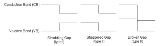
 Semiconductor interfaces can be organized into three types of heterojunctions: straddling gap (type I), staggered gap (type II) or broken gap (type III) as seen in the figure above. There are three relevant material properties for classifying a given junction and understanding the charge dynamics at a heterojunction: band gap, electron affinity and work function. The energy difference between the valence band
(VB) and conduction band
(CB), called the band gap
, is anywhere from 0eV for a metal (there is no gap) to over 4eV for an insulator
. The work function
of a material is the energy difference between the Fermi energy
(chemical equilibrium energy) and the vacuum level (where electron removal occurs). Finally the electron affinity
of each material is needed which is the energy difference between the conduction band and the vacuum level. Calculating energy band offsets for an ideal heterojunction is straightforward given these material properties using the Anderson's rule
. The conduction band offset depends only on the electron affinity difference between the two semiconductors: Then using the change in band gap: The valence band offset is simply given by: Which confirms the trivial relationship between band offsets and band gap difference: In Anderson's idealized model these material parameters are unchanged when the materials are brought together to form an interface, so it ignores the quantum size effect, defect states and other perturbations which may or may not be the result of imperfect crystal lattice matches (more on lattice considerations below). When two materials are brought together and allowed to reach chemical/thermal equilibrium the fermi level in each material aligns and is constant throughout the system. To the extent that they are able, electrons in the materials leave some regions (depletion) and build up in others (accumulation) in order to find equilibrium. When this occurs a certain amount of band bending occurs near the interface. This total band bending can be quantified with the built in potential given by: Where and In most cases where the materials are undoped, these terms are just half the band gap. Otherwise, can be calculated with typical solid state device calculations and depends on dopant concentrations and temperature. The built in potential gives the degree to which band bending occurs but tells us nothing about how this happens spatially. In order to know over what distance the bending occurs in which materials, we must know the density of states
and state occupation given by the Fermi-Dirac distribution.NEWLINE
NEWLINENEWLINE
In real semiconductor heterojunctions, Anderson's model fails to predict actual band offsets. Some material parameters are given in the table on the right which do not match experimental results using Anderson's rule. This idealized model ignores the fact that each material is made up of a crystal lattice whose electrical properties depend on a periodic arrangement of atoms. This periodicity is broken at the heterojunction interface to varying degrees. In cases where both materials have the same lattice, they may still have differing lattice constant
s which give rise to crystal strain which changes the band energies. In other cases the strain is relaxed via dislocation
s and other interfacial defects which also change the band energies. A common anion rule was proposed which guesses that since the valence band is related to anionic states, materials with the same anions should have very small valence band offsets. This however did not explain the data but is related to the trend that two materials with different anions tend to have larger valence band
offsets than conduction band
offsets. Tersoff proposed a model based on more familiar metal-semiconductor junction
s where the conduction band offset is given by the difference in Schottky barrier
height. This model includes a dipole
later at the interface between the two semiconductors which arises from electron tunneling from the conduction band of one material into the gap of the other. This model agrees well with systems where both materials are closely lattice matched such as GaAs
/AlGaAs. Anderson's rule overestimates the offset in the conduction band of the commercially important type two offset GaAs/AlAs system with from the data above. It has been shown that for the actual ratio is closer . This is known as the 60:40 rule and applies to heterojunctions of GaAs with all compositions of AlGaAs. The typical method for measuring band offsets is by calculating them from measuring exciton
energies in the luminescence
spectra.
s, a quantum well
can be fabricated due to difference in band structure. In order to calculate the static energy level
s within the achieved quantum well, understanding variation or mismatch of the effective mass across the heterojunction becomes substantial. The quantum well defined in the heterojunction can be treated as a finite well potential with width of . Addition to that, in 1966, Conley et al. and BenDaniel and Duke reported boundary condition for the envelope function
in quantum well, known as BenDaniel-Duke boundary condition. According to them, the envelope function in fabricated quantum well must satisfy boundary condition which states are both continuous in interface regions. Using the Schrödinger equation
for a finite well with width of and center at 0, the equation for the achieved quantum well can be written as: NEWLINE
energies.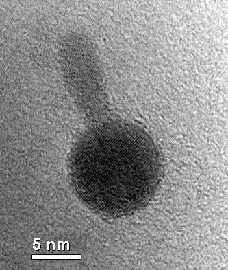 In quantum dot
s the band energies are dependent on crystal size due to the quantum size effects. This enables band offset engineering in nanoscale heterostructures. It is possible to use the same materials but change the type of junction, say from straddling (type I) to staggered (type II), by changing the size or thickness of the crystals involved. The most common nanoscale heterostructure system is core\shell CdSe\ZnS
which is a straddling gap (type I) offset. In this system the much larger band gap
ZnS passivates the surface of the fluorescent CdSe core thereby increasing the quantum efficiency
of the luminescence
. There is an added bonus of increased thermal stability
due to the stronger bonds
in the ZnS shell as suggested by its larger band gap. Since CdSe and ZnS both grow in the zincblende crystal phase and are closely lattice matched, core shell growth is preferred. In other systems or under different growth conditions it may be possible to grow anisotropic structures such as the one seen in the image on the right. It has been shown that the driving force for charge transfer between conduction band
s in these structures is the conduction band offset. By decreasing the size of CdSe nanocrystal
s grown on TiO2
, Robel et al. found that electrons transferred faster from the higher CdSe conduction band into TiO2. In CdSe the quantum size effect is much more pronounced in the conduction band due to the smaller effective mass than in the valence band, and this is the case with most semiconductors. Consequently, engineering the conduction band offset is typically much easier with nanoscale heterojunctions. For staggered (type II) offset nanoscale heterojunctions, photoinduced charge separation
can occur since there the lowest energy state for holes
may be on one side of the junction where as the lowest energy for electrons is on the opposite side. It has been suggested that anisotropic staggered gap (type II) nanoscale heterojunctions may be used for photocatalysis
, specifically for water splitting
with solar energy.
s was first proposed in 1963 when Herbert Kroemer
, thought of as the father of this field, suggested that population inversion
could be greatly enhanced by heterostructures. By incorporating a smaller direct band gap material like GaAs
between two larger band gap layers like AlAs
, carriers
can be confined so that lasing can occur at room temperature
with low threshold currents. It took many years for the material science of heterostructure fabrication to catch up with Kroemer's ideas but now it is the industry standard. It was later discovered that the band gap could be controlled by taking advantage of the quantum size effects in quantum well
heterostructures. Furthermore, heterostructures can be used as waveguide
s to the index step
which occurs at the interface, another major advantage to their use in semiconductor lasers. Semiconductor diode lasers used in CD & DVD
players and fiber optic transceiver
s are manufactured using alternating layers of various III-V
and II-VI
compound semiconductor
s to form lasing heterostructures. When a heterojunction is used as the base-emitter junction of a bipolar junction transistor
, extremely high forward gain
and low reverse gain result. This translates into very good high frequency operation (values in tens to hundreds of GHz) and low leakage currents. This device is called a heterojunction bipolar transistor
(HBT). Heterojunctions are used in high electron mobility transistors
(HEMT) which can operate at significantly higher frequencies (over 500 GHz). The proper doping profile and band alignment gives rise to extremely high electron mobilities
by creating a two dimensional electron gas
within a dopant free region
where very little scattering
can occur.
(MBE) or chemical vapor deposition
(CVD) technologies into order to precisely control the deposition thickness and create a planar interface. MBE and CVD tend to be very complex and expensive compared to traditional silicon
device fabrication.
Layer
Layer may refer to:* A layer of archaeological deposits in an excavation* A layer hen, a hen raised to produce eggs* Stratum, a layer of rock or soil with internally consistent characteristics...
s or regions of dissimilar crystalline semiconductor
Semiconductor
A semiconductor is a material with electrical conductivity due to electron flow intermediate in magnitude between that of a conductor and an insulator. This means a conductivity roughly in the range of 103 to 10−8 siemens per centimeter...
s. These semiconducting materials have unequal band gap
Band gap
In solid state physics, a band gap, also called an energy gap or bandgap, is an energy range in a solid where no electron states can exist. In graphs of the electronic band structure of solids, the band gap generally refers to the energy difference between the top of the valence band and the...
s as opposed to a homojunction
Homojunction
A homojunction is a semiconductor interface that occurs between layers of similar semiconductor material, these materials have equal band gaps but typically have different doping. In most practical cases a homojunction occurs at the interface between an n-type and p-type semiconductor such as...
. It is often advantageous to engineer the electronic energy bands in many solid state device applications including semiconductor lasers, solar cells and transistors ("heterotransistors") to name a few. The combination of multiple heterojunctions together in a device is called a heterostructure although the two terms are commonly used interchangeably. The requirement that each material be a semiconductor with unequal band gaps is somewhat loose especially on small length scales where electronic properties depend on spatial properties. A more modern definition may be to say that a heterojunction is the interface between any two solid-state materials including crystalline and amorphous structures of metallic, insulating, fast ion conductor
Fast ion conductor
In solid-state ionics, fast ion conductors, also known as solid electrolytes and superionic conductors, are materials that act as solid state ion conductors and are used primarily in solid oxide fuel cells. As solid electrolytes they conduct due to the movement of ions through voids, or empty...
and semiconducting material. In 2000, the Nobel Prize
Nobel Prize
The Nobel Prizes are annual international awards bestowed by Scandinavian committees in recognition of cultural and scientific advances. The will of the Swedish chemist Alfred Nobel, the inventor of dynamite, established the prizes in 1895...
in physics was awarded jointly to Herbert Kroemer
Herbert Kroemer
Herbert Kroemer , a professor of electrical and computer engineering at the University of California, Santa Barbara, received his Ph.D. in theoretical physics in 1952 from the University of Göttingen, Germany, with a dissertation on hot electron effects in the then-new transistor, setting the stage...
(University of California at Santa Barbara, California, USA) and Zhores I. Alferov (A.F. Ioffe Physico-Technical Institute, St. Petersburg, Russia) for "developing semiconductor heterostructures used in high-speed- and opto-electronics"
Energy band offsets for ideal heterojunctions
Valence band
In solids, the valence band is the highest range of electron energies in which electrons are normally present at absolute zero temperature....
(VB) and conduction band
Conduction band
In the solid-state physics field of semiconductors and insulators, the conduction band is the range of electron energies, higher than that of the valence band, sufficient to free an electron from binding with its individual atom and allow it to move freely within the atomic lattice of the material...
(CB), called the band gap
Band gap
In solid state physics, a band gap, also called an energy gap or bandgap, is an energy range in a solid where no electron states can exist. In graphs of the electronic band structure of solids, the band gap generally refers to the energy difference between the top of the valence band and the...
, is anywhere from 0eV for a metal (there is no gap) to over 4eV for an insulator
Electrical insulation
thumb|250px|[[Coaxial Cable]] with dielectric insulator supporting a central coreThis article refers to electrical insulation. For insulation of heat, see Thermal insulation...
. The work function
Work function
In solid-state physics, the work function is the minimum energy needed to remove an electron from a solid to a point immediately outside the solid surface...
of a material is the energy difference between the Fermi energy
Fermi energy
The Fermi energy is a concept in quantum mechanics usually referring to the energy of the highest occupied quantum state in a system of fermions at absolute zero temperature....
(chemical equilibrium energy) and the vacuum level (where electron removal occurs). Finally the electron affinity
Electron affinity
The Electron affinity of an atom or molecule is defined as the amount of energy released when an electron is added to a neutral atom or molecule to form a negative ion....
of each material is needed which is the energy difference between the conduction band and the vacuum level. Calculating energy band offsets for an ideal heterojunction is straightforward given these material properties using the Anderson's rule
Anderson's rule
Anderson's rule is used for the construction of energy band diagrams of the heterojunction between two semiconductor materials. It is also referred to as the electron affinity rule. Anderson's rule was first described by R. L...
. The conduction band offset depends only on the electron affinity difference between the two semiconductors: Then using the change in band gap: The valence band offset is simply given by: Which confirms the trivial relationship between band offsets and band gap difference: In Anderson's idealized model these material parameters are unchanged when the materials are brought together to form an interface, so it ignores the quantum size effect, defect states and other perturbations which may or may not be the result of imperfect crystal lattice matches (more on lattice considerations below). When two materials are brought together and allowed to reach chemical/thermal equilibrium the fermi level in each material aligns and is constant throughout the system. To the extent that they are able, electrons in the materials leave some regions (depletion) and build up in others (accumulation) in order to find equilibrium. When this occurs a certain amount of band bending occurs near the interface. This total band bending can be quantified with the built in potential given by: Where and In most cases where the materials are undoped, these terms are just half the band gap. Otherwise, can be calculated with typical solid state device calculations and depends on dopant concentrations and temperature. The built in potential gives the degree to which band bending occurs but tells us nothing about how this happens spatially. In order to know over what distance the bending occurs in which materials, we must know the density of states
Density of states
In solid-state and condensed matter physics, the density of states of a system describes the number of states per interval of energy at each energy level that are available to be occupied by electrons. Unlike isolated systems, like atoms or molecules in gas phase, the density distributions are not...
and state occupation given by the Fermi-Dirac distribution.
Energy band offsets in real heterojunctions
NEWLINE| NEWLINE | (eV) | NEWLINE(eV) | NEWLINE
|---|---|---|
| GaAs | NEWLINE1.43 | NEWLINE4.07 | NEWLINE
| AlAs | NEWLINE2.16 | NEWLINE2.62 | NEWLINE
| GaP | NEWLINE2.21 | NEWLINE4.3 | NEWLINE
| InAs | NEWLINE.36 | NEWLINE4.9 | NEWLINE
| InP | NEWLINE1.35 | NEWLINE4.35 | NEWLINE
| Si | NEWLINE1.12 | NEWLINE4.05[ref 7] | NEWLINE
| Ge | NEWLINE.66 | NEWLINE4.0[ref 7] | NEWLINE
| From ref | NEWLINENEWLINE | NEWLINE |
Lattice constant
The lattice constant [or lattice parameter] refers to the constant distance between unit cells in a crystal lattice. Lattices in three dimensions generally have three lattice constants, referred to as a, b, and c. However, in the special case of cubic crystal structures, all of the constants are...
s which give rise to crystal strain which changes the band energies. In other cases the strain is relaxed via dislocation
Dislocation
In materials science, a dislocation is a crystallographic defect, or irregularity, within a crystal structure. The presence of dislocations strongly influences many of the properties of materials...
s and other interfacial defects which also change the band energies. A common anion rule was proposed which guesses that since the valence band is related to anionic states, materials with the same anions should have very small valence band offsets. This however did not explain the data but is related to the trend that two materials with different anions tend to have larger valence band
Valence band
In solids, the valence band is the highest range of electron energies in which electrons are normally present at absolute zero temperature....
offsets than conduction band
Conduction band
In the solid-state physics field of semiconductors and insulators, the conduction band is the range of electron energies, higher than that of the valence band, sufficient to free an electron from binding with its individual atom and allow it to move freely within the atomic lattice of the material...
offsets. Tersoff proposed a model based on more familiar metal-semiconductor junction
Metal-semiconductor junction
In solid-state physics, a metal–semiconductor junction is a type of junction in which a metal comes in close contact with a semiconductor material...
s where the conduction band offset is given by the difference in Schottky barrier
Schottky barrier
A Schottky barrier, named after Walter H. Schottky, is a potential barrier formed at a metal–semiconductor junction which has rectifying characteristics, suitable for use as a diode...
height. This model includes a dipole
Dipole
In physics, there are several kinds of dipoles:*An electric dipole is a separation of positive and negative charges. The simplest example of this is a pair of electric charges of equal magnitude but opposite sign, separated by some distance. A permanent electric dipole is called an electret.*A...
later at the interface between the two semiconductors which arises from electron tunneling from the conduction band of one material into the gap of the other. This model agrees well with systems where both materials are closely lattice matched such as GaAs
Gaas
Gaas is a commune in the Landes department in Aquitaine in south-western France....
/AlGaAs. Anderson's rule overestimates the offset in the conduction band of the commercially important type two offset GaAs/AlAs system with from the data above. It has been shown that for the actual ratio is closer . This is known as the 60:40 rule and applies to heterojunctions of GaAs with all compositions of AlGaAs. The typical method for measuring band offsets is by calculating them from measuring exciton
Exciton
An exciton is a bound state of an electron and hole which are attracted to each other by the electrostatic Coulomb force. It is an electrically neutral quasiparticle that exists in insulators, semiconductors and some liquids...
energies in the luminescence
Luminescence
Luminescence is emission of light by a substance not resulting from heat; it is thus a form of cold body radiation. It can be caused by chemical reactions, electrical energy, subatomic motions, or stress on a crystal. This distinguishes luminescence from incandescence, which is light emitted by a...
spectra.
Effective mass mismatch at heterojunctions
When a heterojunction is formed by two different semiconductorSemiconductor
A semiconductor is a material with electrical conductivity due to electron flow intermediate in magnitude between that of a conductor and an insulator. This means a conductivity roughly in the range of 103 to 10−8 siemens per centimeter...
s, a quantum well
Quantum well
A quantum well is a potential well with only discrete energy values.One technology to create quantization is to confine particles, which were originally free to move in three dimensions, to two dimensions, forcing them to occupy a planar region...
can be fabricated due to difference in band structure. In order to calculate the static energy level
Energy level
A quantum mechanical system or particle that is bound -- that is, confined spatially—can only take on certain discrete values of energy. This contrasts with classical particles, which can have any energy. These discrete values are called energy levels...
s within the achieved quantum well, understanding variation or mismatch of the effective mass across the heterojunction becomes substantial. The quantum well defined in the heterojunction can be treated as a finite well potential with width of . Addition to that, in 1966, Conley et al. and BenDaniel and Duke reported boundary condition for the envelope function
Envelope (mathematics)
In geometry, an envelope of a family of curves in the plane is a curve that is tangent to each member of the family at some point. Classically, a point on the envelope can be thought of as the intersection of two "adjacent" curves, meaning the limit of intersections of nearby curves...
in quantum well, known as BenDaniel-Duke boundary condition. According to them, the envelope function in fabricated quantum well must satisfy boundary condition which states are both continuous in interface regions. Using the Schrödinger equation
Schrödinger equation
The Schrödinger equation was formulated in 1926 by Austrian physicist Erwin Schrödinger. Used in physics , it is an equation that describes how the quantum state of a physical system changes in time....
for a finite well with width of and center at 0, the equation for the achieved quantum well can be written as: NEWLINE
- NEWLINE
- NEWLINE
- NEWLINENEWLINENEWLINE
- NEWLINE
- NEWLINE
- NEWLINE
- .
- NEWLINE
- NEWLINE
- NEWLINE
- .
- NEWLINE
- NEWLINE
- NEWLINE
- .
- NEWLINE
- NEWLINE
- NEWLINE
- .
- NEWLINE
- NEWLINE
- NEWLINE
- .
- NEWLINE
- NEWLINE
- NEWLINE
- NEWLINE
- NEWLINE
- NEWLINE
Ground state
The ground state of a quantum mechanical system is its lowest-energy state; the energy of the ground state is known as the zero-point energy of the system. An excited state is any state with energy greater than the ground state...
energies.
Nanoscale heterojunctions
Quantum dot
A quantum dot is a portion of matter whose excitons are confined in all three spatial dimensions. Consequently, such materials have electronic properties intermediate between those of bulk semiconductors and those of discrete molecules. They were discovered at the beginning of the 1980s by Alexei...
s the band energies are dependent on crystal size due to the quantum size effects. This enables band offset engineering in nanoscale heterostructures. It is possible to use the same materials but change the type of junction, say from straddling (type I) to staggered (type II), by changing the size or thickness of the crystals involved. The most common nanoscale heterostructure system is core\shell CdSe\ZnS
ZNS
ZNS or ZnS may refer to:In entertainment:* ZNS , a popular entertainer in China and Chinese speaking parts of the world...
which is a straddling gap (type I) offset. In this system the much larger band gap
Band gap
In solid state physics, a band gap, also called an energy gap or bandgap, is an energy range in a solid where no electron states can exist. In graphs of the electronic band structure of solids, the band gap generally refers to the energy difference between the top of the valence band and the...
ZnS passivates the surface of the fluorescent CdSe core thereby increasing the quantum efficiency
Quantum efficiency
Quantum efficiency is a quantity defined for a photosensitive device such as photographic film or a charge-coupled device as the percentage of photons hitting the photoreactive surface that will produce an electron–hole pair. It is an accurate measurement of the device's electrical sensitivity to...
of the luminescence
Luminescence
Luminescence is emission of light by a substance not resulting from heat; it is thus a form of cold body radiation. It can be caused by chemical reactions, electrical energy, subatomic motions, or stress on a crystal. This distinguishes luminescence from incandescence, which is light emitted by a...
. There is an added bonus of increased thermal stability
Thermal stability
Thermal stability is the stability of a molecule at high temperatures; i.e. a molecule with more stability has more resistance to decomposition at high temperatures....
due to the stronger bonds
Chemical bond
A chemical bond is an attraction between atoms that allows the formation of chemical substances that contain two or more atoms. The bond is caused by the electromagnetic force attraction between opposite charges, either between electrons and nuclei, or as the result of a dipole attraction...
in the ZnS shell as suggested by its larger band gap. Since CdSe and ZnS both grow in the zincblende crystal phase and are closely lattice matched, core shell growth is preferred. In other systems or under different growth conditions it may be possible to grow anisotropic structures such as the one seen in the image on the right. It has been shown that the driving force for charge transfer between conduction band
Conduction band
In the solid-state physics field of semiconductors and insulators, the conduction band is the range of electron energies, higher than that of the valence band, sufficient to free an electron from binding with its individual atom and allow it to move freely within the atomic lattice of the material...
s in these structures is the conduction band offset. By decreasing the size of CdSe nanocrystal
Nanocrystal
B. D. Fahlman has described a nanocrystal as any nanomaterial with at least one dimension ≤ 100nm and that is singlecrystalline.-Summary:More properly, any material with a dimension of less than 1 micrometre, i.e., 1000 nanometers, should be referred to as a nanoparticle, not a nanocrystal...
s grown on TiO2
Titanium dioxide
Titanium dioxide, also known as titanium oxide or titania, is the naturally occurring oxide of titanium, chemical formula . When used as a pigment, it is called titanium white, Pigment White 6, or CI 77891. Generally it comes in two different forms, rutile and anatase. It has a wide range of...
, Robel et al. found that electrons transferred faster from the higher CdSe conduction band into TiO2. In CdSe the quantum size effect is much more pronounced in the conduction band due to the smaller effective mass than in the valence band, and this is the case with most semiconductors. Consequently, engineering the conduction band offset is typically much easier with nanoscale heterojunctions. For staggered (type II) offset nanoscale heterojunctions, photoinduced charge separation
Photoinduced charge separation
Photoinduced charge separation is the process of an electron in an atom being excited to a higher energy level by the absorption of a photon and then leaving the atom to a nearby electron acceptor.-Rutherford model:...
can occur since there the lowest energy state for holes
Electron hole
An electron hole is the conceptual and mathematical opposite of an electron, useful in the study of physics, chemistry, and electrical engineering. The concept describes the lack of an electron at a position where one could exist in an atom or atomic lattice...
may be on one side of the junction where as the lowest energy for electrons is on the opposite side. It has been suggested that anisotropic staggered gap (type II) nanoscale heterojunctions may be used for photocatalysis
Photocatalysis
In chemistry, photocatalysis is the acceleration of a photoreaction in the presence of a catalyst. In catalysed photolysis, light is absorbed by an adsorbed substrate. In photogenerated catalysis, the photocatalytic activity depends on the ability of the catalyst to create electron–hole pairs,...
, specifically for water splitting
Water splitting
Water splitting is the general term for a chemical reaction in which water is separated into oxygen and hydrogen. Efficient and economical water splitting would be a key technology component of a hydrogen economy. Various techniques for water splitting have been issued in water splitting patents in...
with solar energy.
Applications
Using heterojunctions in laserLaser
A laser is a device that emits light through a process of optical amplification based on the stimulated emission of photons. The term "laser" originated as an acronym for Light Amplification by Stimulated Emission of Radiation...
s was first proposed in 1963 when Herbert Kroemer
Herbert Kroemer
Herbert Kroemer , a professor of electrical and computer engineering at the University of California, Santa Barbara, received his Ph.D. in theoretical physics in 1952 from the University of Göttingen, Germany, with a dissertation on hot electron effects in the then-new transistor, setting the stage...
, thought of as the father of this field, suggested that population inversion
Population inversion
In physics, specifically statistical mechanics, a population inversion occurs when a system exists in state with more members in an excited state than in lower energy states...
could be greatly enhanced by heterostructures. By incorporating a smaller direct band gap material like GaAs
Gaas
Gaas is a commune in the Landes department in Aquitaine in south-western France....
between two larger band gap layers like AlAs
Alas
The term alas may refer to:* an interjection used to express regret, sorrow, or grief.* in geomorphology, a steep-sided depression formed by the melting of permafrost; it may contain a lake.* in zoology, a wing or winglike body part....
, carriers
Charge carriers in semiconductors
There are two recognized types of charge carriers in semiconductors. One of them is electrons, which carry negative electric charge. In addition, it is convenient to treat the traveling vacancies in the valence-band electron population as the second type of charge carriers, which carry a positive...
can be confined so that lasing can occur at room temperature
Room temperature
-Comfort levels:The American Society of Heating, Refrigerating and Air-Conditioning Engineers has listings for suggested temperatures and air flow rates in different types of buildings and different environmental circumstances. For example, a single office in a building has an occupancy ratio per...
with low threshold currents. It took many years for the material science of heterostructure fabrication to catch up with Kroemer's ideas but now it is the industry standard. It was later discovered that the band gap could be controlled by taking advantage of the quantum size effects in quantum well
Quantum well
A quantum well is a potential well with only discrete energy values.One technology to create quantization is to confine particles, which were originally free to move in three dimensions, to two dimensions, forcing them to occupy a planar region...
heterostructures. Furthermore, heterostructures can be used as waveguide
Waveguide
A waveguide is a structure which guides waves, such as electromagnetic waves or sound waves. There are different types of waveguides for each type of wave...
s to the index step
Step-index profile
For an optical fiber, a step-index profile is a refractive index profile characterized by a uniform refractive index within the core and a sharp decrease in refractive index at the core-cladding interface so that the cladding is of a lower refractive index. The step-index profile corresponds to a...
which occurs at the interface, another major advantage to their use in semiconductor lasers. Semiconductor diode lasers used in CD & DVD
DVD
A DVD is an optical disc storage media format, invented and developed by Philips, Sony, Toshiba, and Panasonic in 1995. DVDs offer higher storage capacity than Compact Discs while having the same dimensions....
players and fiber optic transceiver
Transceiver
A transceiver is a device comprising both a transmitter and a receiver which are combined and share common circuitry or a single housing. When no circuitry is common between transmit and receive functions, the device is a transmitter-receiver. The term originated in the early 1920s...
s are manufactured using alternating layers of various III-V
Semiconductor materials
Semiconductor materials are nominally small band gap insulators. The defining property of a semiconductor material is that it can be doped with impurities that alter its electronic properties in a controllable way...
and II-VI
Semiconductor materials
Semiconductor materials are nominally small band gap insulators. The defining property of a semiconductor material is that it can be doped with impurities that alter its electronic properties in a controllable way...
compound semiconductor
Compound semiconductor
A compound semiconductor is a semiconductor compound composed of elements from two or more different groups of the periodic table . These semiconductors typically form in groups 13-16 ,...
s to form lasing heterostructures. When a heterojunction is used as the base-emitter junction of a bipolar junction transistor
Bipolar junction transistor
|- align = "center"| || PNP|- align = "center"| || NPNA bipolar transistor is a three-terminal electronic device constructed of doped semiconductor material and may be used in amplifying or switching applications. Bipolar transistors are so named because their operation involves both electrons...
, extremely high forward gain
Gain
In electronics, gain is a measure of the ability of a circuit to increase the power or amplitude of a signal from the input to the output. It is usually defined as the mean ratio of the signal output of a system to the signal input of the same system. It may also be defined on a logarithmic scale,...
and low reverse gain result. This translates into very good high frequency operation (values in tens to hundreds of GHz) and low leakage currents. This device is called a heterojunction bipolar transistor
Heterojunction bipolar transistor
The heterojunction bipolar transistor is a type of bipolar junction transistor which uses differing semiconductor materials for the emitter and base regions, creating a heterojunction. The HBT improves on the BJT in that it that can handle signals of very high frequencies, up to several hundred...
(HBT). Heterojunctions are used in high electron mobility transistors
HEMT
High electron mobility transistor , also known as heterostructure FET or modulation-doped FET , is a field effect transistor incorporating a junction between two materials with different band gaps as the channel instead of a doped region, as is generally the case for MOSFET...
(HEMT) which can operate at significantly higher frequencies (over 500 GHz). The proper doping profile and band alignment gives rise to extremely high electron mobilities
Electron mobility
In solid-state physics, the electron mobility characterizes how quickly an electron can move through a metal or semiconductor, when pulled by an electric field. In semiconductors, there is an analogous quantity for holes, called hole mobility...
by creating a two dimensional electron gas
2DEG
A two-dimensional electron gas is a gas of electrons free to move in two dimensions, but tightly confined in the third. This tight confinement leads to quantized energy levels for motion in that direction, which can then be ignored for most problems. Thus the electrons appear to be a 2D sheet...
within a dopant free region
Intrinsic semiconductor
An intrinsic semiconductor, also called an undoped semiconductor or i-type semiconductor, is a pure semiconductor without any significant dopant species present. The number of charge carriers is therefore determined by the properties of the material itself instead of the amount of impurities...
where very little scattering
Scattering
Scattering is a general physical process where some forms of radiation, such as light, sound, or moving particles, are forced to deviate from a straight trajectory by one or more localized non-uniformities in the medium through which they pass. In conventional use, this also includes deviation of...
can occur.
Fabrication
Heterojunction manufacturing generally requires the use of molecular beam epitaxyMolecular beam epitaxy
Molecular beam epitaxy is one of several methods of depositing single crystals. It was invented in the late 1960s at Bell Telephone Laboratories by J. R. Arthur and Alfred Y. Cho.-Method:...
(MBE) or chemical vapor deposition
Chemical vapor deposition
Chemical vapor deposition is a chemical process used to produce high-purity, high-performance solid materials. The process is often used in the semiconductor industry to produce thin films. In a typical CVD process, the wafer is exposed to one or more volatile precursors, which react and/or...
(CVD) technologies into order to precisely control the deposition thickness and create a planar interface. MBE and CVD tend to be very complex and expensive compared to traditional silicon
Silicon
Silicon is a chemical element with the symbol Si and atomic number 14. A tetravalent metalloid, it is less reactive than its chemical analog carbon, the nonmetal directly above it in the periodic table, but more reactive than germanium, the metalloid directly below it in the table...
device fabrication.
See also
NEWLINE- NEWLINE
- Anderson's ruleAnderson's ruleAnderson's rule is used for the construction of energy band diagrams of the heterojunction between two semiconductor materials. It is also referred to as the electron affinity rule. Anderson's rule was first described by R. L...NEWLINE
- Band gapBand gapIn solid state physics, a band gap, also called an energy gap or bandgap, is an energy range in a solid where no electron states can exist. In graphs of the electronic band structure of solids, the band gap generally refers to the energy difference between the top of the valence band and the...NEWLINE
- Heterojunction bipolar transistorHeterojunction bipolar transistorThe heterojunction bipolar transistor is a type of bipolar junction transistor which uses differing semiconductor materials for the emitter and base regions, creating a heterojunction. The HBT improves on the BJT in that it that can handle signals of very high frequencies, up to several hundred...NEWLINE
- HEMTHEMTHigh electron mobility transistor , also known as heterostructure FET or modulation-doped FET , is a field effect transistor incorporating a junction between two materials with different band gaps as the channel instead of a doped region, as is generally the case for MOSFET...NEWLINE
- HomojunctionHomojunctionA homojunction is a semiconductor interface that occurs between layers of similar semiconductor material, these materials have equal band gaps but typically have different doping. In most practical cases a homojunction occurs at the interface between an n-type and p-type semiconductor such as...NEWLINE
- Multijunction NEWLINE
- p-n junctionP-n junctionA p–n junction is formed at the boundary between a P-type and N-type semiconductor created in a single crystal of semiconductor by doping, for example by ion implantation, diffusion of dopants, or by epitaxy .If two separate pieces of material were used, this would...