

Threshold voltage
Encyclopedia


MOSFET
The metal–oxide–semiconductor field-effect transistor is a transistor used for amplifying or switching electronic signals. The basic principle of this kind of transistor was first patented by Julius Edgar Lilienfeld in 1925...
is usually defined as the gate voltage where an inversion layer forms at the interface between the insulating layer (oxide) and the substrate (body) of the transistor
Transistor
A transistor is a semiconductor device used to amplify and switch electronic signals and power. It is composed of a semiconductor material with at least three terminals for connection to an external circuit. A voltage or current applied to one pair of the transistor's terminals changes the current...
. The purpose of the inversion layer's forming is to allow the flow of electrons through the gate-source junction. The creation of this layer is described next.
In an n-MOSFET the substrate of the transistor is composed of p-type silicon (see doping (semiconductor)
Doping (semiconductor)
In semiconductor production, doping intentionally introduces impurities into an extremely pure semiconductor for the purpose of modulating its electrical properties. The impurities are dependent upon the type of semiconductor. Lightly and moderately doped semiconductors are referred to as extrinsic...
), which has positively charged mobile holes as carriers. When a positive voltage
Voltage
Voltage, otherwise known as electrical potential difference or electric tension is the difference in electric potential between two points — or the difference in electric potential energy per unit charge between two points...
is applied on the gate, an electric field
Electric field
In physics, an electric field surrounds electrically charged particles and time-varying magnetic fields. The electric field depicts the force exerted on other electrically charged objects by the electrically charged particle the field is surrounding...
causes the holes to be repelled from the interface, creating a depletion region
Depletion region
In semiconductor physics, the depletion region, also called depletion layer, depletion zone, junction region or the space charge region, is an insulating region within a conductive, doped semiconductor material where the mobile charge carriers have diffused away, or have been forced away by an...
containing immobile negatively charged acceptor ions. A further increase in the gate voltage eventually causes electrons to appear at the interface, in what is called an inversion layer, or channel. Historically the gate voltage at which the electron density at the interface is the same as the hole density in the neutral bulk material is called the threshold voltage. Practically speaking the threshold voltage is the voltage at which there are sufficient electrons in the inversion layer to make a low resistance conducting path between the MOSFET source and drain.
In the figures, the source (left side) and drain (right side) are labeled n+ to indicate heavily doped (blue) n-regions. The depletion layer dopant is labeled NA− to indicate that the ions in the (pink) depletion layer are negatively charged and there are very few holes. In the (red) bulk the number of holes p = NA making the bulk charge neutral.
If the gate voltage is below the threshold voltage (top figure), the transistor is turned off and ideally there is no current
Electric current
Electric current is a flow of electric charge through a medium.This charge is typically carried by moving electrons in a conductor such as wire...
from the drain to the source of the transistor. In fact, there is a current even for gate biases below threshold (subthreshold leakage
Subthreshold leakage
The Subthreshold conduction or the subthreshold leakage or the subthreshold drain current is the current that flows between the source and drain of a MOSFET when the transistor is in subthreshold region, or weak-inversion region, that is, for gate-to-source voltages below the threshold voltage. The...
) current, although it is small and varies exponentially with gate bias.
If the gate voltage is above the threshold voltage (lower figure), the transistor is turned on, due to there being many electrons in the channel at the oxide-silicon interface, creating a low-resistance channel where charge can flow from drain to source. For voltages significantly above threshold, this situation is called strong inversion. The channel is tapered when VD > 0 because the voltage drop due to the current in the resistive channel reduces the oxide field supporting the channel as the drain is approached.
In modern devices the threshold voltage is a much less clear-cut parameter subject to variation with the biases applied to the device; see drain induced barrier lowering.
Body effect
The body effect describes the changes in the threshold voltage by the change in , the source-bulk voltage. Since the body influences the threshold voltage (when it is not tied to the source), it can be thought of as a second gate, and is sometimes referred to as the "back gate"; the body effect is sometimes called the "back-gate effect".
For an enhancement mode, n-mos MOSFET body effect upon threshold voltage is computed according to the Shichman-Hodges model (accurate for very old technology) using the following equation.

where
 is the threshold voltage when substrate bias is present,
  is the source-to-body substrate bias,
  is the surface potential, and
  is threshold voltage for zero substrate bias,
 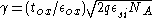 is the body effect parameter,
  is oxide thickness,
  is oxide permitivity,
  is the permitivity of silicon,
  is a doping concentration,
  is the charge of an electron.
Dependence on oxide thickness
In a given technology node, such as the 90 nanometer90 nanometer
The 90 nm process refers to the level of CMOS process technology that was reached in the 2002–2003 timeframe, by most leading semiconductor companies, like Intel, AMD, Infineon, Texas Instruments, IBM, and TSMC....
CMOS process, threshold voltage depends on the choice of oxide and on oxide thickness. Using the body formulas above,
 is directly proportional to
  , and
, and  , which is the parameter for oxide thickness.
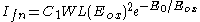
Thus, the thinner the oxide thickness, the lower the threshold voltage. While this may seem to be an improvement, it is not without cost; for the thinner the oxide thickness, the higher the subthreshold leakage
Subthreshold leakage
The Subthreshold conduction or the subthreshold leakage or the subthreshold drain current is the current that flows between the source and drain of a MOSFET when the transistor is in subthreshold region, or weak-inversion region, that is, for gate-to-source voltages below the threshold voltage. The...
current flowing through the device will be. Consequently, the design specification for 90 nanometer gate oxide thickness was set at 1 nanometer to control the leakage current. This kind of tunneling, called Fowler-Nordheim Tunneling.
where
 and
and  are constants and
  is the electric field across the gate oxide.
Before scaling the design features down to 90 nanometers, a dual oxide approach for creating the oxide thickness was a common solution to this issue. With a 90 nanometer process technology, a triple oxide approach has been adopted in some cases. One standard thin oxide is used for most transistors, another for I/O driver cells, and a third for memory and pass transistor cells. These differences are based purely on the characteristics of oxide thickness on threshold voltage of CMOS technologies.
Dependence on temperature
As with the case of oxide thickness affecting threshold voltage, temperature has an effect on the threshold voltage of a CMOS device. Expanding on part of the equation in the body effect section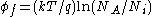
where
 is Boltzmann's constant,
  is Temperature,
  is the charge of an electron,
  is a doping parameter and
  is the intrinsic doping parameter for the substrate.
We see that the surface potential has a direct relationship with the temperature. Looking above, that while the threshold voltage does not have a direct relationship but is not independent of the effects. On average this variation is between −4 mV/°C and −2 mV/°C depending on doping level. For a change of 30 °C this results in significant variation from the 500mV design parameter commonly used for the 90 nanometer technology node.
External links
- Online lecture on: Threshold Voltage and MOSFET Capacitances by Dr. Lundstrom
See also
- MOSFET operation
- Channel length modulationChannel length modulationOne of several short channel effects in MOSFET scaling, channel length modulation is a shortening of the length of the inverted channel region with increase in drain bias for large drain biases...
- Drain-induced barrier lowering