

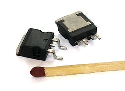
Power MOSFET
Encyclopedia
MOSFET
The metal–oxide–semiconductor field-effect transistor is a transistor used for amplifying or switching electronic signals. The basic principle of this kind of transistor was first patented by Julius Edgar Lilienfeld in 1925...
) designed to handle significant power levels. Compared to the other power semiconductor device
Power semiconductor device
Power semiconductor devices are semiconductor devices used as switches or rectifiers in power electronic circuits . They are also called power devices or when used in integrated circuits, called power ICs....
s (IGBT, Thyristor
Thyristor
A thyristor is a solid-state semiconductor device with four layers of alternating N and P-type material. They act as bistable switches, conducting when their gate receives a current trigger, and continue to conduct while they are forward biased .Some sources define silicon controlled rectifiers and...
...), its main advantages are high commutation speed and good efficiency at low voltages. It shares with the IGBT an isolated gate that makes it easy to drive.
It was made possible by the evolution of CMOS
CMOS
Complementary metal–oxide–semiconductor is a technology for constructing integrated circuits. CMOS technology is used in microprocessors, microcontrollers, static RAM, and other digital logic circuits...
technology, developed for manufacturing Integrated circuit
Integrated circuit
An integrated circuit or monolithic integrated circuit is an electronic circuit manufactured by the patterned diffusion of trace elements into the surface of a thin substrate of semiconductor material...
s in the late 1970s. The power MOSFET shares its operating principle with its low-power counterpart, the lateral MOSFET
MOSFET
The metal–oxide–semiconductor field-effect transistor is a transistor used for amplifying or switching electronic signals. The basic principle of this kind of transistor was first patented by Julius Edgar Lilienfeld in 1925...
.
The power MOSFET is the most widely used low-voltage (i.e. less than 200 V) switch. It can be found in most power supplies
Power supply
A power supply is a device that supplies electrical energy to one or more electric loads. The term is most commonly applied to devices that convert one form of electrical energy to another, though it may also refer to devices that convert another form of energy to electrical energy...
, DC to DC converter
DC to DC converter
A DC-to-DC converter is an electronic circuit which converts a source of direct current from one voltage level to another. It is a class of power converter.- Usage :...
s, and low voltage motor controller
Motor controller
A motor controller is a device or group of devices that serves to govern in some predetermined manner the performance of an electric motor. A motor controller might include a manual or automatic means for starting and stopping the motor, selecting forward or reverse rotation, selecting and...
s.
Basic structure
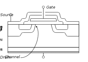
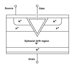
The cross section of a VDMOS (see figure 1) shows the "verticality" of the device: It can be seen that the source electrode is placed over the drain, resulting in a current mainly vertical when the transistor is in the on-state. The "diffusion
Diffusion
Molecular diffusion, often called simply diffusion, is the thermal motion of all particles at temperatures above absolute zero. The rate of this movement is a function of temperature, viscosity of the fluid and the size of the particles...
" in VDMOS refers to the manufacturing process: the P wells (see figure 1) are obtained by a diffusion process (actually a double diffusion process to get the P and N+ regions, hence the name double diffused).
Power MOSFETs have a different structure than the lateral MOSFET
MOSFET
The metal–oxide–semiconductor field-effect transistor is a transistor used for amplifying or switching electronic signals. The basic principle of this kind of transistor was first patented by Julius Edgar Lilienfeld in 1925...
: as with most power devices, their structure is vertical and not planar. In a planar structure, the current and breakdown voltage
Breakdown voltage
The breakdown voltage of an insulator is the minimum voltage that causes a portion of an insulator to become electrically conductive.The breakdown voltage of a diode is the minimum reverse voltage to make the diode conduct in reverse...
ratings are both functions of the channel dimensions (respectively width and length of the channel), resulting in inefficient use of the "silicon estate". With a vertical structure, the voltage rating of the transistor is a function of the doping
Doping (semiconductor)
In semiconductor production, doping intentionally introduces impurities into an extremely pure semiconductor for the purpose of modulating its electrical properties. The impurities are dependent upon the type of semiconductor. Lightly and moderately doped semiconductors are referred to as extrinsic...
and thickness of the N epitaxial
Epitaxy
Epitaxy refers to the deposition of a crystalline overlayer on a crystalline substrate, where the overlayer is in registry with the substrate. In other words, there must be one or more preferred orientations of the overlayer with respect to the substrate for this to be termed epitaxial growth. The...
layer (see cross section), while the current rating is a function of the channel width. This makes possible for the transistor to sustain both high blocking voltage and high current within a compact piece of silicon.
It is worth noting that power MOSFETs with lateral structure exist. They are mainly used in high-end audio amplifiers. Their advantage is a better behaviour in the saturated region (corresponding to the linear region of a bipolar transistor
Bipolar junction transistor
|- align = "center"| || PNP|- align = "center"| || NPNA bipolar transistor is a three-terminal electronic device constructed of doped semiconductor material and may be used in amplifying or switching applications. Bipolar transistors are so named because their operation involves both electrons...
) than the vertical MOSFETs. Vertical MOSFETs are designed for switching applications, so they are only used in On or Off states.
On-state resistance
MOSFET
The metal–oxide–semiconductor field-effect transistor is a transistor used for amplifying or switching electronic signals. The basic principle of this kind of transistor was first patented by Julius Edgar Lilienfeld in 1925...
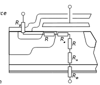
for a discussion on operation modes), it exhibits a resistive behaviour between the drain and source terminals. It can be seen in figure 2 that this resistance (called RDSon for "drain to source resistance in on-state") is the sum of many elementary contributions:
- RS is the source resistance. It represents all resistances between the source terminal of the package to the channel of the MOSFET: resistance of the wire bondsWire bondingWire bonding is the primary method of making interconnections between an integrated circuit and a printed circuit board during semiconductor device fabrication. Although less common, wire bonding can be used to connect an IC to other electronics or to connect from one PCB to another...
, of the source metallisation, and of the N+ wells; - Rch. This is the channel resistance. It is inversely proportional to the channel width, and for a given die size, to the channel density. The channel resistance is one of the main contributors to the RDSon of low-voltage MOSFETs, and intensive work has been carried out to reduce their cell size in order to increase the channel density;
- Ra is the access resistance. It represents the resistance of the epitaxial zone directly under the gate electrode, where the direction of the current changes from horizontal (in the channel) to vertical (to the drain contact);
- RJFET is the detrimental effect of the cell size reduction mentioned above: the P implantations (see figure 1) form the gates of a parasitic JFETJFETThe junction gate field-effect transistor is the simplest type of field-effect transistor. It can be used as an electronically-controlled switch or as a voltage-controlled resistance. Electric charge flows through a semiconducting channel between "source" and "drain" terminals...
transistor that tend to reduce the width of the current flow; - Rn is the resistance of the epitaxial layer. As the role of this layer is to sustain the blocking voltage, Rn is directly related to the voltage rating of the device. A high voltage MOSFET requires a thick, low-doped layer (i.e. highly resistive), whereas a low-voltage transistor only requires a thin layer with a higher doping level (i.e. less resistive). As a result, Rn is the main factor responsible for the resistance of high-voltage MOSFETs;
- RD is the equivalent of RS for the drain. It represents the resistance of the transistor substrate (note that the cross section in figure 1 is not at scale, the bottom N+ layer is actually the thickest) and of the package connections.
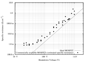
Breakdown voltage/on-state resistance trade-off
Epitaxy
Epitaxy refers to the deposition of a crystalline overlayer on a crystalline substrate, where the overlayer is in registry with the substrate. In other words, there must be one or more preferred orientations of the overlayer with respect to the substrate for this to be termed epitaxial growth. The...
layer and the N+ substrate). When this highly non-symmetrical structure is reverse-biased, the space-charge region extends principally on the light-doped side, i.e. over the N- layer. This means that this layer has to withstand most of the MOSFET's OFF-state drain-to-source voltage.
However, when the MOSFET is in the ON-state, this N- layer has no function. Furthermore, as it is a lightly doped region, its intrinsic resistivity is non-negligible and adds to the MOSFET's ON-state Drain-to-Source Resistance (RDSon) (this is the Rn resistance in figure 2).
Two main parameters govern both the breakdown voltage and the RDSon of the transistor: the doping level and the thickness of the N- epitaxial
Epitaxy
Epitaxy refers to the deposition of a crystalline overlayer on a crystalline substrate, where the overlayer is in registry with the substrate. In other words, there must be one or more preferred orientations of the overlayer with respect to the substrate for this to be termed epitaxial growth. The...
layer. The thicker the layer and the lower its doping level, the higher the breakdown voltage. On the contrary, the thinner the layer and the higher the doping level, the lower the RDSon (and therefore the lower the conduction losses of the MOSFET). Therefore, it can be seen that there is a trade-off in the design of a MOSFET, between its voltage rating and its ON-state resistance. This is demonstrated by the plot in figure 3.
Body diode
It can be seen in figure 1 that the source metallization connects both the N+ and P implantations, although the operating principle of the MOSFET only requires the source to be connected to the N+ zone. However, if it were, this would result in a floating P zone between the N-doped source and drain, which is equivalent to a NPN transistor with a non-connected base. Under certain conditions (under high drain current, when the on-state drain to source voltage is in the order of some volts), this parasitic NPN transistor would be triggered, making the MOSFET uncontrollable. The connection of the P implantation to the source metallization shorts the base of the parasitic transistor to its emitter (the source of the MOSFET) and thus prevents spurious latching.This solution, however, creates a diode
Diode
In electronics, a diode is a type of two-terminal electronic component with a nonlinear current–voltage characteristic. A semiconductor diode, the most common type today, is a crystalline piece of semiconductor material connected to two electrical terminals...
between the drain (cathode) and the source (anode) of the MOSFET, making it able to block current in only one direction.
Switching operation
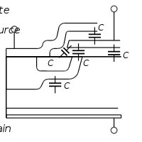
The only intrinsic limitation in commutation speed is due to the internal capacitances of the MOSFET (see figure 4). These capacitances must be charged or discharged when the transistor switches. This can be a relatively slow process because the current that flows through the gate capacitances is limited by the external driver circuit. This circuit will actually dictate the commutation speed of the transistor (assuming the power circuit has sufficiently low inductance).
Capacitances
In the MOSFETs datasheetDatasheet
thumb|A floppy disk controller datasheet.A datasheet, data sheet, or spec sheet is a document summarizing the performance and other technical characteristics of a product, machine, component , material, a subsystem or software in sufficient detail to be used by a design engineer to integrate the...
s, the capacitances are often named Ciss (input capacitance, drain and source terminal shorted), Coss (output capacitance, gate and source shorted), and Crss (reverse transfer capacitance, gate and source shorted). The relationship between these capacitances and those described below is:
Where CGS, CGD and CDS are respectively the gate-to-source, gate-to-drain and drain-to-source capacitances (see below). Manufacturers prefer to quote Ciss, Coss and Crss because they can be directly measured on the transistor. However, as CGS, CGD and CDS are closer to the physical meaning, they will be used in the remaining of this article.
Gate to source capacitance
The CGS capacitance is constituted by the parallel connection of CoxN+, CoxP and Coxm (see figure 4). As the N+ and P regions are highly doped, the two former capacitances can be considered as constant. Coxm is the capacitance between the (polysilicon) gate and the (metal) source electrode, so it is also constant. Therefore, it is common practice to consider CGS as a constant capacitance, i.e. its value does not depend on the transistor state.Gate to drain capacitance
The CGD capacitance can be seen as the connection in series of two elementary capacitances. The first one is the oxide capacitance (CoxD), constituted by the gate electrode, the silicon dioxide and the top of the N epitaxial layer. It has a constant value. The second capacitance (CGDj) is caused by the extension of the space-charge zone when the MOSFET is in off-state (see the section Blocking Voltage). Therefore, it is dependent upon the drain to source voltage. From this, the value of CGD is: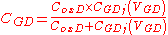
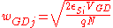
The width of the space-charge region is given by
where
 is the permittivity
Permittivity
In electromagnetism, absolute permittivity is the measure of the resistance that is encountered when forming an electric field in a medium. In other words, permittivity is a measure of how an electric field affects, and is affected by, a dielectric medium. The permittivity of a medium describes how...
of the Silicon, q is the electron
Electron
The electron is a subatomic particle with a negative elementary electric charge. It has no known components or substructure; in other words, it is generally thought to be an elementary particle. An electron has a mass that is approximately 1/1836 that of the proton...
charge, and N is the doping
Doping (semiconductor)
In semiconductor production, doping intentionally introduces impurities into an extremely pure semiconductor for the purpose of modulating its electrical properties. The impurities are dependent upon the type of semiconductor. Lightly and moderately doped semiconductors are referred to as extrinsic...
level. The value of CGDj can be approximated using the expression of the plane capacitor
Capacitor
A capacitor is a passive two-terminal electrical component used to store energy in an electric field. The forms of practical capacitors vary widely, but all contain at least two electrical conductors separated by a dielectric ; for example, one common construction consists of metal foils separated...
:
Where AGD is the surface area of the gate-drain overlap. Therefore, it comes:
It can be seen that CGDj (and thus CGD) is a capacitance which value is dependent upon the gate to drain voltage. As this voltage increases, the capacitance decreases. When the MOSFET is in on-state, CGDj is shunted, so the gate to drain capacitance remains equal to CoxD, a constant value.
Drain to source capacitance
As the source metallization overlaps the P-wells (see figure 1), the drain and source terminals are separated by a P-N junctionP-n junction
A p–n junction is formed at the boundary between a P-type and N-type semiconductor created in a single crystal of semiconductor by doping, for example by ion implantation, diffusion of dopants, or by epitaxy .If two separate pieces of material were used, this would...
. Therefore, CDS is the junction capacitance. This is a non-linear capacitance, and its value can be calculated using the same equation as for CGDj.
Other dynamic elements

Packaging inductances
To operate, the MOSFET must be connected to the external circuit, most of the time using wire bondingWire bonding
Wire bonding is the primary method of making interconnections between an integrated circuit and a printed circuit board during semiconductor device fabrication. Although less common, wire bonding can be used to connect an IC to other electronics or to connect from one PCB to another...
(although alternative techniques are investigated). These connection exhibit a parasitic inductance, which is in no way specific to the MOSFET technology, but has important effects because of its high commutation speed. Parasitic inductances tend to maintain their current constant and generate overvoltage during the transistor turn off, resulting in increasing commutation losses.
A parasitic inductance can be associated with each terminal of the MOSFET. They have different effects:
- the gate inductance has little influence (assuming it is lower than some hundreds of nanohenries), because the current gradients on the gate are relatively slow. In some cases, however, the gate inductance and the input capacitance of the transistor can constitute an oscillator. This must be avoided as it results in very high commutation losses (up to the destruction of the device). On a typical design, parasitic inductances are kept low enough to prevent this phenomenon;
- the drain inductance tends to reduce the drain voltage when the MOSFET turns on, so it reduces turn on losses. However, as it creates an overvoltage during turn-off, it increases turn-off losses;
- the source parasitic inductance has the same behaviour as the drain inductance, plus a feedbackFeedbackFeedback describes the situation when output from an event or phenomenon in the past will influence an occurrence or occurrences of the same Feedback describes the situation when output from (or information about the result of) an event or phenomenon in the past will influence an occurrence or...
effect that makes commutation last longer, thus increasing commutation losses.- at the beginning of a fast turn-on, due to the source inductance, the voltage at the source (on the die) will be able to jump up as well as the gate voltage; the internal VGS voltage will remain low for a longer time, therefore delaying turn-on.
- at the beginning of a fast turn-off, as current through the source inductance decreases sharply, the resulting voltage across it goes negative (with respect to the lead outside the package) raising the internal VGS voltage, keeping the MOSFET on, and therefore delaying turn-off.
Gate oxide breakdown
The gate oxide is very thin (100 nm or less), so it can only sustain a limited voltage. In the datasheetDatasheet
thumb|A floppy disk controller datasheet.A datasheet, data sheet, or spec sheet is a document summarizing the performance and other technical characteristics of a product, machine, component , material, a subsystem or software in sufficient detail to be used by a design engineer to integrate the...
s, manufacturers often state a maximum gate to source voltage, around 20 V, and exceeding this limit can result in destruction of the component. Furthermore, a high gate to source voltage reduces significantly the lifetime of the MOSFET, with little to no advantage on RDSon reduction.
Maximum drain to source voltage
Power MOSFETs have a maximum specified drain to source voltage, beyond which breakdownAvalanche breakdown
Avalanche breakdown is a phenomenon that can occur in both insulating and semiconducting materials. It is a form of electric current multiplication that can allow very large currents within materials which are otherwise good insulators. It is a type of electron avalanche...
may occur. Exceeding the breakdown voltage causes the device to conduct, potentially damaging it and other circuit elements due to excessive power dissipation.
Maximum drain current
The drain current must generally stay below a certain specified value (maximum continuous drain current). It can reach higher values for very short durations of time (maximum pulsed drain current, sometimes specified for various pulse durations). The drain current is limited by heating due to resistive lossesJoule heating
Joule heating, also known as ohmic heating and resistive heating, is the process by which the passage of an electric current through a conductor releases heat. It was first studied by James Prescott Joule in 1841. Joule immersed a length of wire in a fixed mass of water and measured the temperature...
in internal components such as bond wires
Wire bonding
Wire bonding is the primary method of making interconnections between an integrated circuit and a printed circuit board during semiconductor device fabrication. Although less common, wire bonding can be used to connect an IC to other electronics or to connect from one PCB to another...
, and other phenomena such as electromigration
Electromigration
Electromigration is the transport of material caused by the gradual movement of the ions in a conductor due to the momentum transfer between conducting electrons and diffusing metal atoms. The effect is important in applications where high direct current densities are used, such as in...
in the metal layer.
Maximum temperature
The junction temperatureJunction temperature
Junction temperature is the highest temperature of the actual semiconductor in an electronic device. In operation it is higher than case temperature and the temperature of the part's exterior...
(TJ) of the MOSFET must stay under a specified maximum value for the device to function reliably, determined by MOSFET die layout and packaging materials. The packaging often limits the maximum junction temperature, due to the molding compound and (where used) epoxy characteristics.
The maximum operating ambient temperature is determined by the power dissipation and thermal resistance. The junction-to-case thermal resistance is intrinsic to the device and package; the case-to-ambient thermal resistance is largely dependent on the board/mounting layout, heatsinking area and air/fluid flow.
The type of power dissipation, whether continuous or pulsed, affects the maximum operating temperature
Operating temperature
An operating temperature is the temperature at which an electrical or mechanical device operates. The device will operate effectively within a specified temperature range which varies based on the device function and application context, and ranges from the minimum operating temperature to the...
, due to thermal capacitance characteristics; in general, the lower the frequency of pulses for a given power dissipation, the higher maximum operating ambient temperature, due to allowing a longer interval for the device to cool down. Models, such as a Foster Network, can be used to analyze temperature dynamics from power transients.
Safe operating area
The safe operating areaSafe operating area
For power semiconductor devices , the safe operating area is defined as the voltage and current conditions over which the device can be expected to operate without self-damage....
defines the combined ranges of drain current and drain to source voltage the power MOSFET is able to handle without damage. It is represented graphically as an area in the plane defined by these two parameters. Both drain current and drain to source voltage must stay below their respective maximum values, but their product must also stay below the maximum power dissipation the device is able to handle. Thus the device cannot be operated at both its specified maximum drain current and maximum drain to source voltage.
Latch-up (LU)
The equivalent circuit for a MOSFET consist of one MOSFET in parallel with a parasitic BJT (Bipolar Junction TransistorBipolar junction transistor
|- align = "center"| || PNP|- align = "center"| || NPNA bipolar transistor is a three-terminal electronic device constructed of doped semiconductor material and may be used in amplifying or switching applications. Bipolar transistors are so named because their operation involves both electrons...
). If the BJT turns ON, it cannot be turned off since the gate has no control over it. This phenomenon is known as 'latch-up'
Latchup
Latchup is a term used in the realm of integrated circuits to describe a particular type of short circuit which can occur in an improperly designed circuit...
, which can lead to device destruction. The BJT can be turned on due to a voltage drop across the p-type body region. To avoid latch-up, the body and the source are typically short circuited within the device package.
Cellular structure
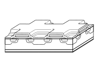
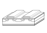
To minimize cost and size, it is valuable to keep the transistor's die area size as small as possible. Therefore, optimizations have been developed to increase the width of the channel surface area (i.e. increase the "channel density"). They mainly consist of creating cellular structures repeated over the whole area of the MOSFET die. Several shapes have been proposed for these cells, the most famous being the International Rectifier's "Hexfet" (hexagonal shape).
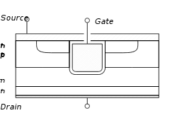
Another way to increase the channel density is to reduce the size of the elementary structure. This allows for more cells in a given surface area, and therefore more channel width. However, as the cell size shrinks, it becomes more difficult to ensure proper contact of every cell. To overcome this, a "strip" structure is often used (see figure). It is less efficient than a cellular structure of equivalent resolution in terms of channel density, but can cope with smaller pitch.
P-substrate power MOSFET
A P-substrate MOSFET (often referred to as PMOS) is a MOSFET with opposite doping types (N instead of P and P instead of N in the cross-section in figure 1). This MOSFET is made using a P-type substrate, with a P- epitaxy. As the channel sits in a N-region, this transistor is turned on by a negative gate to source voltage. This makes it desirable in a buck converterBuck converter
A buck converter is a step-down DC to DC converter. Its design is similar to the step-up boost converter, and like the boost converter it is a switched-mode power supply that uses two switches , an inductor and a capacitor....
, where one of the terminals of the switch is connected to the high side of the input voltage: with a N-MOSFET, this configuration requires to apply to the gate a voltage equal to
 , whereas no voltage over
  is required with a P-MOSFET.
The main disadvantage of this type of MOSFET is the poor on-state performance: it uses holes as charge carrier
Charge carrier
In physics, a charge carrier is a free particle carrying an electric charge, especially the particles that carry electric currents in electrical conductors. Examples are electrons and ions...
s, which have a much lower mobility
Electron mobility
In solid-state physics, the electron mobility characterizes how quickly an electron can move through a metal or semiconductor, when pulled by an electric field. In semiconductors, there is an analogous quantity for holes, called hole mobility...
than electrons. As resistivity
Resistivity
Electrical resistivity is a measure of how strongly a material opposes the flow of electric current. A low resistivity indicates a material that readily allows the movement of electric charge. The SI unit of electrical resistivity is the ohm metre...
is directly related to mobility, a given PMOS will have a
 three times higher than a N-MOSFET with the same dimensions.
VMOS
VMOS
VMOS is an acronym for Vertical Metal Oxide Semiconductor . Vmos is also used to describe the V-groove shape vertically cut into the substrate material metal oxide semiconductor transistor....
has a V-groove at the gate region and was used for the first commercial devices .
UMOS (also called Trench-MOS)
CoolMOS
Especially for voltages beyond 500 V some manufacturers, most notably Infineon TechnologiesInfineon Technologies
Infineon Technologies AG is a German semiconductor manufacturer and was founded on April 1, 1999, when the semiconductor operations of the parent company Siemens AG were spun off to form a separate legal entity. , Infineon has 25,149 employees worldwide...
, have begun to use a charge compensation principle. Thus the resistance in the epitaxial
Epitaxy
Epitaxy refers to the deposition of a crystalline overlayer on a crystalline substrate, where the overlayer is in registry with the substrate. In other words, there must be one or more preferred orientations of the overlayer with respect to the substrate for this to be termed epitaxial growth. The...
layer as biggest contributor in high voltage MOSFETs can be reduced by a factor of greater than 5.
See also
- Power semiconductor devicePower semiconductor devicePower semiconductor devices are semiconductor devices used as switches or rectifiers in power electronic circuits . They are also called power devices or when used in integrated circuits, called power ICs....
- IGBTInsulated gate bipolar transistorThe insulated gate bipolar transistor or IGBT is a three-terminal power semiconductor device primarily used as an electronic switch and in newer devices is noted for combining high efficiency and fast switching...
- Power electronicsPower electronicsPower electronics is the application of solid-state electronics for the control and conversion of electric power.-Introduction:Power electronic converters can be found wherever there is a need to modify a form of electrical energy...