

Ion implantation
Encyclopedia
Materials science
Materials science is an interdisciplinary field applying the properties of matter to various areas of science and engineering. This scientific field investigates the relationship between the structure of materials at atomic or molecular scales and their macroscopic properties. It incorporates...
research. The ions can introduce both a chemical change in the target, in that they can introduce a different element than the target or induce a nuclear transmutation
Nuclear transmutation
Nuclear transmutation is the conversion of one chemical element or isotope into another. In other words, atoms of one element can be changed into atoms of other element by 'transmutation'...
, and a structural change, in that the crystal structure
Crystal structure
In mineralogy and crystallography, crystal structure is a unique arrangement of atoms or molecules in a crystalline liquid or solid. A crystal structure is composed of a pattern, a set of atoms arranged in a particular way, and a lattice exhibiting long-range order and symmetry...
of the target can be damaged or even destroyed by the energetic collision cascade
Collision cascade
A collision cascade is a set of nearby adjacent energetic collisions of atoms induced by an energetic particle in a solid or liquid....
s.
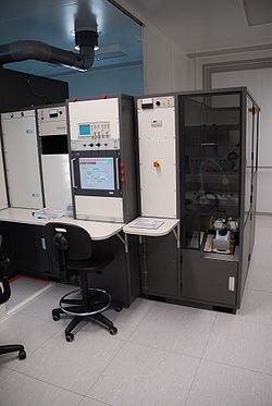
General principle
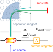
Ion source
An ion source is an electro-magnetic device that is used to create charged particles. These are used primarily to form ions for mass spectrometers, optical emission spectrometers, particle accelerators, ion implanters and ion engines.- Electron ionization :...
, where ions of the desired element are produced, an
accelerator
Particle accelerator
A particle accelerator is a device that uses electromagnetic fields to propel charged particles to high speeds and to contain them in well-defined beams. An ordinary CRT television set is a simple form of accelerator. There are two basic types: electrostatic and oscillating field accelerators.In...
, where the ions are electrostatically accelerated to a high energy, and a target chamber, where the ions impinge on a target, which is the material to be implanted. Thus ion implantation is a special case of
particle radiation
Particle radiation
Particle radiation is the radiation of energy by means of fast-moving subatomic particles. Particle radiation is referred to as a particle beam if the particles are all moving in the same direction, similar to a light beam....
.
Each ion is typically a single atom or molecule, and thus the actual amount of material implanted in the target is the integral over time of the ion current. This amount is called the dose. The currents supplied by implanters are typically small (microamperes), and thus the dose which can be implanted in a reasonable amount of time is small. Therefore, ion implantation finds application in cases where the amount of chemical change required is small.
Typical ion energies are in the range of 10 to 500 keV
Electronvolt
In physics, the electron volt is a unit of energy equal to approximately joule . By definition, it is equal to the amount of kinetic energy gained by a single unbound electron when it accelerates through an electric potential difference of one volt...
(1,600 to 80,000 aJ). Energies in the range 1 to 10 keV (160 to 1,600 aJ) can be used, but result in a penetration of only a few nanometers or less. Energies lower than this result in very little damage to the target, and fall under the designation ion beam deposition
Ion beam deposition
Ion Beam Deposition is a process of applying materials to a target through the application of an ion beam.thumb|Ion beam deposition setup with mass separator...
. Higher energies can also be used: accelerators capable of 5 MeV (800,000 aJ) are common. However, there is often great structural damage to the target, and because the depth distribution is broad, the net composition change at any point in the target will be small.
The energy of the ions, as well as the ion species and the composition of the target determine the depth of penetration of the ions in the solid: A monoenergetic ion beam will generally have a broad depth distribution. The average penetration depth is called the range of the ions. Under typical circumstances ion ranges will be between 10 nanometers and 1 micrometer. Thus, ion implantation is especially useful in cases where the chemical or structural change is desired to be near the surface of the target. Ions gradually lose their energy as they travel through the solid, both from occasional collisions with target atoms (which cause abrupt energy transfers) and from a mild drag from overlap of electron orbitals, which is a continuous process. The loss of ion energy in the target is called stopping
Stopping power (particle radiation)
In passing through matter, fast charged particles ionize the atoms or molecules which they encounter. Thus, the fast particles gradually lose energy in many small steps. Stopping power is defined as the average energy loss of the particle per unit path length, measured for example in MeV/cm...
and can be simulated with the binary collision approximation
Binary collision approximation
The binary collision approximation signifies a method used in ion irradiation physics to enable efficient computer simulation of the penetration depth and...
method.
DopingDoping (semiconductor)In semiconductor production, doping intentionally introduces impurities into an extremely pure semiconductor for the purpose of modulating its electrical properties. The impurities are dependent upon the type of semiconductor. Lightly and moderately doped semiconductors are referred to as extrinsic...
The introduction of dopants in a semiconductor is most common application of ion implantation. Dopant ions such as boron, phosphorus or arsenic are generally created from a gas source, so that the purity of the source can be very high. These gases tend to be very hazardous. When implanted in a semiconductor, each dopant atom can create a charge carrier in the semiconductor after annealingAnnealing (metallurgy)
Annealing, in metallurgy and materials science, is a heat treatment wherein a material is altered, causing changes in its properties such as strength and hardness. It is a process that produces conditions by heating to above the recrystallization temperature, maintaining a suitable temperature, and...
. A hole
Electron hole
An electron hole is the conceptual and mathematical opposite of an electron, useful in the study of physics, chemistry, and electrical engineering. The concept describes the lack of an electron at a position where one could exist in an atom or atomic lattice...
can be created for a p-type dopant, and an electron for an n-type dopant. This modifies the conductivity of the semiconductor in its vicinity. The technique is used, for example, for adjusting the threshold of a MOSFET
MOSFET
The metal–oxide–semiconductor field-effect transistor is a transistor used for amplifying or switching electronic signals. The basic principle of this kind of transistor was first patented by Julius Edgar Lilienfeld in 1925...
.
Ion implantation was developed as a method of producing the p-n junction of photovoltaic devices in the late 1970s and early 1980s, along with the use of pulsed-electron beam for rapid annealing, although it has not to date been used for commercial production.
Silicon on insulatorSilicon on insulatorSilicon on insulator technology refers to the use of a layered silicon-insulator-silicon substrate in place of conventional silicon substrates in semiconductor manufacturing, especially microelectronics, to reduce parasitic device capacitance and thereby improving performance...
One prominent method for preparing silicon on insulator (SOI) substrates from conventional siliconSilicon
Silicon is a chemical element with the symbol Si and atomic number 14. A tetravalent metalloid, it is less reactive than its chemical analog carbon, the nonmetal directly above it in the periodic table, but more reactive than germanium, the metalloid directly below it in the table...
substrates is the SIMOX (Separation by IMplantation of OXygen) process, wherein a buried high dose oxygen implant is converted to silicon oxide by a high temperature annealing
Annealing (metallurgy)
Annealing, in metallurgy and materials science, is a heat treatment wherein a material is altered, causing changes in its properties such as strength and hardness. It is a process that produces conditions by heating to above the recrystallization temperature, maintaining a suitable temperature, and...
process.
Mesotaxy
Mesotaxy is the term for the growth of a crystallographically matching phase underneath the surface of the host crystal (compare to epitaxyEpitaxy
Epitaxy refers to the deposition of a crystalline overlayer on a crystalline substrate, where the overlayer is in registry with the substrate. In other words, there must be one or more preferred orientations of the overlayer with respect to the substrate for this to be termed epitaxial growth. The...
, which is the growth of the matching phase on the surface of a substrate). In this process, ions are implanted at a high enough energy and dose into a material to create a layer of a second phase, and the temperature is controlled so that the crystal structure of the target is not destroyed. The crystal orientation of the layer can be engineered to match that of the target, even though the exact crystal structure and lattice constant may be very different. For example, after the implantation of nickel ions into a silicon wafer, a layer of nickel silicide can be grown in which the crystal orientation of the silicide matches that of the silicon.
Tool steel toughening
Nitrogen or other ions can be implanted into a tool steel target (drill bits, for example). The structural change caused by the implantation produces a surface compression in the steel, which prevents crack propagation and thus makes the material more resistant to fracture. The chemical change can also make the tool more resistant to corrosion.Surface finishing
In some applications, for example prosthetic devices such as artificial joints, it is desired to have surfaces very resistant to both chemical corrosion and wear due to friction. Ion implantation is used in such cases to engineer the surfaces of such devices for more reliable performance. As in the case of tool steels, the surface modification caused by ion implantation includes both a surface compression which prevents crack propagation and an alloying of the surface to make it more chemically resistant to corrosion.Ion beam mixing
Ion implantation can be used to achieve ion beam mixingIon Beam Mixing
Ion Beam Mixing is a process for adhering two multilayers, especially a substrate and deposited surface layer. The process involves bombarding layered samples with doses of ion radiation in order to promote mixing at the interface, and generally serves as a means of preparing electrical junctions,...
, i.e. mixing up atoms of different elements at an interface. This may be useful for achieving graded interfaces or strengthening adhesion between layers of immiscible materials.
Crystallographic damage
Each individual ion produces many point defectsCrystallographic defect
Crystalline solids exhibit a periodic crystal structure. The positions of atoms or molecules occur on repeating fixed distances, determined by the unit cell parameters. However, the arrangement of atom or molecules in most crystalline materials is not perfect...
in the target crystal on impact such as vacancies and interstitials. Vacancies are crystal lattice points unoccupied by an atom: in this case the ion collides with a target atom, resulting in transfer of a significant amount of energy to the target atom such that it leaves its crystal site. This target atom then itself becomes a projectile in the solid, and can cause successive collision events
Collision cascade
A collision cascade is a set of nearby adjacent energetic collisions of atoms induced by an energetic particle in a solid or liquid....
.
Interstitials result when such atoms (or the original ion itself) come to rest in the solid, but find no vacant space in the lattice to reside. These point defects can migrate and cluster with each other, resulting in dislocation
Dislocation
In materials science, a dislocation is a crystallographic defect, or irregularity, within a crystal structure. The presence of dislocations strongly influences many of the properties of materials...
loops and other defects.
Damage recovery
Because ion implantation causes damage to the crystal structure of the target which is often unwanted, ion implantation processing is often followed by a thermal annealing. This can be referred to as damage recovery.Amorphization
The amount of crystallographic damage can be enough to completely amorphize the surface of the target: i.e. it can become an amorphous solidAmorphous solid
In condensed matter physics, an amorphous or non-crystalline solid is a solid that lacks the long-range order characteristic of a crystal....
(such a solid produced from a melt is called a glass
Glass
Glass is an amorphous solid material. Glasses are typically brittle and optically transparent.The most familiar type of glass, used for centuries in windows and drinking vessels, is soda-lime glass, composed of about 75% silica plus Na2O, CaO, and several minor additives...
). In some cases, complete amorphization of a target is preferable to a highly defective crystal: An amorphized film can be regrown at a lower temperature than required to anneal a highly damaged crystal.
Sputtering
Some of the collision events result in atoms being ejected (sputteredSputtering
Sputtering is a process whereby atoms are ejected from a solid target material due to bombardment of the target by energetic particles. It is commonly used for thin-film deposition, etching and analytical techniques .-Physics of sputtering:...
) from the surface, and thus ion implantation will slowly etch away a surface. The effect is only appreciable for very large doses.
Ion channelling

Silicon
Silicon is a chemical element with the symbol Si and atomic number 14. A tetravalent metalloid, it is less reactive than its chemical analog carbon, the nonmetal directly above it in the periodic table, but more reactive than germanium, the metalloid directly below it in the table...
and other diamond cubic
Diamond cubic
The diamond cubic crystal structure is a repeating pattern of 8 atoms that certain materials may adopt as they solidify. While the first known example was diamond, other elements in group IV also adopt this structure, including tin, the semiconductors silicon and germanium, and silicon/germanium...
materials. This effect is called ion channelling, and, like all the channelling
Channelling (physics)
Channelling is the process that constrains the path of a charged particle in a crystalline solid.Many physical phenomena can occur when a charged particle is incident upon a solid target, e.g., elastic scattering, inelastic energy-loss processes, secondary-electron emission, electromagnetic...
effects, is highly nonlinear, with small variations from perfect orientation resulting in extreme differences in implantation depth. For this reason, most implantation is carried out a few degrees off-axis, where tiny alignment errors will have more predictable effects.
Ion channelling can be used directly in Rutherford backscattering and related techniques as an analytical method to determine the amount and depth profile of damage in crystalline thin film materials.
Hazardous Materials Note
In the ion implantation semiconductor fabrication process of wafersWafer (electronics)
A wafer is a thin slice of semiconductor material, such as a silicon crystal, used in the fabrication of integrated circuits and other microdevices...
, it is important for the workers to minimize their exposure to the toxic materials are
used in the ion implanter process. Such hazardous elements, solid source and gasses are used, such as arsine
Arsine
Arsine is the chemical compound with the formula AsH3. This flammable, pyrophoric, and highly toxic gas is one of the simplest compounds of arsenic...
and phosphine
Phosphine
Phosphine is the compound with the chemical formula PH3. It is a colorless, flammable, toxic gas. Pure phosphine is odourless, but technical grade samples have a highly unpleasant odor like garlic or rotting fish, due to the presence of substituted phosphine and diphosphine...
. For this reason, the semiconductor fabrication
Semiconductor fabrication
Semiconductor device fabrication is the process used to create the integrated circuits that are present in everyday electrical and electronic devices. It is a multiple-step sequence of photolithographic and chemical processing steps during which electronic circuits are gradually created on a wafer...
facilities are highly automated, and may feature negative pressure gas bottles safe delivery system (SDS). Other elements may include antimony
Antimony
Antimony is a toxic chemical element with the symbol Sb and an atomic number of 51. A lustrous grey metalloid, it is found in nature mainly as the sulfide mineral stibnite...
, arsenic
Arsenic
Arsenic is a chemical element with the symbol As, atomic number 33 and relative atomic mass 74.92. Arsenic occurs in many minerals, usually in conjunction with sulfur and metals, and also as a pure elemental crystal. It was first documented by Albertus Magnus in 1250.Arsenic is a metalloid...
, phosphorus
Phosphorus
Phosphorus is the chemical element that has the symbol P and atomic number 15. A multivalent nonmetal of the nitrogen group, phosphorus as a mineral is almost always present in its maximally oxidized state, as inorganic phosphate rocks...
, and boron
Boron
Boron is the chemical element with atomic number 5 and the chemical symbol B. Boron is a metalloid. Because boron is not produced by stellar nucleosynthesis, it is a low-abundance element in both the solar system and the Earth's crust. However, boron is concentrated on Earth by the...
. Residue of these elements show up when the machine is opened to atmosphere, and can also be accumulated and found concentrated in the vacuum pumps hardware. It is important not to expose yourself to these carcinogenic
Carcinogen
A carcinogen is any substance, radionuclide, or radiation that is an agent directly involved in causing cancer. This may be due to the ability to damage the genome or to the disruption of cellular metabolic processes...
, corrosive
Corrosion
Corrosion is the disintegration of an engineered material into its constituent atoms due to chemical reactions with its surroundings. In the most common use of the word, this means electrochemical oxidation of metals in reaction with an oxidant such as oxygen...
, flammable, and toxic
Toxicity
Toxicity is the degree to which a substance can damage a living or non-living organisms. Toxicity can refer to the effect on a whole organism, such as an animal, bacterium, or plant, as well as the effect on a substructure of the organism, such as a cell or an organ , such as the liver...
elements. Many overlapping safety protocols must be used when handling these deadly compounds. Use safety, and read MSDSs
Material safety data sheet
A Material Safety Data Sheet is a form with data regarding the properties of a particular substance....
.
High Voltage Safety
High voltage power supplies in ion implantation equipment can pose a risk of electrocution. In addition, high-energy atomic collisions can, in some cases, generate radionuclidesRadionuclide
A radionuclide is an atom with an unstable nucleus, which is a nucleus characterized by excess energy available to be imparted either to a newly created radiation particle within the nucleus or to an atomic electron. The radionuclide, in this process, undergoes radioactive decay, and emits gamma...
. Operators and maintenance personnel should learn and follow the safety advice of the manufacturer and/or the institution responsible for the equipment. Prior to entry to high voltage area, terminal components must be grounded using a grounding stick. Next, power supplies should be locked in the off state and tagged to prevent unauthorized energizing.
Manufacturers of Ion Implantation Equipment
- Advanced Ion Beam Technology
- Axcelis Technologies
- Complete Ions
- Facilitation Centre for Industrial Plasma Technologies
- Global Technologies, R&D equipment and Service
- Ion Beam Services
- Nissin Ion Equipment
- SemEquip
- SEN Corporation
- Tokyo Electron Limited
- Ulvac Technologies
- Varian Semiconductor Equipment
External links
- SEMI -- a semiconductor standards clearinghouse and trade organization
- Ion Implantation
- James Ziegler's code for simulating ion implantation.