
Copper Indium Gallium Selenide Solar Cells
Encyclopedia
Copper indium gallium selenide
(CuIn1-xGaxSe2 or CIGS) is a direct bandgap semiconductor useful for the manufacture of solar cell
s. Because the material strongly absorbs sunlight, a much thinner film is required than of other semiconductor materials. The CIGS absorber is deposited on a glass backing, along with electrodes to collect current.
CIGS's absorption coefficient is higher than any other semiconductor used for solar modules. Devices made with CIGS belong to the thin-film category of photovoltaics
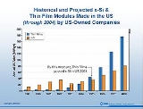
(PV). The market for thin-film PV grew at a 60% annual rate from 2002 to 2007 and is still growing rapidly (Figure 1). Therefore, a strong incentive exists to develop and improve deposition methods for these films that will allow lower cost and increased throughput.
-III
-VI
2 compound semiconductor material composed of copper
, indium
, gallium
, and selenium
. The material is a solid solution
of copper indium selenide (often abbreviated "CIS") and copper gallium selenide, with a chemical formula of CuInxGa(1-x)Se2, where the value of x can vary from 1 (pure copper indium selenide) to 0 (pure copper gallium selenide). It is a tetrahedrally bond
ed semiconductor, with the chalcopyrite
crystal structure. The bandgap varies continuously with x from about 1.0 eV (for copper indium selenide) to about 1.7 eV (for copper gallium selenide).
 CIGS has an exceptionally high absorption coefficient of more than 105/cm for 1.5 eV and higher energy photons. CIGS solar cells with efficiencies greater than 20% have been claimed by both the National Renewable Energy Laboratory (NREL) and the Zentrum für Sonnenenergie und Wasserstoff Forschung (ZSW), which is the record to date for any thin film solar cell
.
or metal foils. A molybdenum
layer is deposited (commonly by sputtering
) which serves as the back contact and to reflect most unabsorbed light back into the absorber. Following Mo deposition a p-type
CIGS absorber layer is grown by one of several unique methods. A thin n-type
buffer layer is added on top of the absorber. The buffer is typically CdS
deposited via chemical bath deposition. The buffer is overlaid with a thin, intrinsic ZnO layer which is capped by a thicker, Al doped ZnO layer. Despite increasing the series resistance, the intrinsic ZnO layer is beneficial to cell performance. The precise mechanism for the improvement is still being debated. The Al doped ZnO serves as a transparent conducting oxide to collect and move electrons out of the cell while absorbing as little light as possible.
The materials based on CuInSe2 that are of interest for photovoltaic applications include several elements from groups I, III and VI in the periodic table. These semiconductors are especially attractive for thin film solar cell application because of their high optical absorption coefficients and versatile optical and electrical characteristics which can in principle be manipulated and tuned for a specific need in a given device.
thin film
s. The best efficiency achieved as of December 2005 was 19.5%. A team at the National Renewable Energy Laboratory
achieved 19.9% new world record efficiency by modifying the CIGS surface and making it look like CIS.
These efficiencies are different from module conversion efficiencies. Two of the leading manufacturers of CIGS thin-film PV have hit new record highs in module conversion efficiencies. The U.S. National Renewable Energy Laboratory has confirmed 13.8% efficiency of a large-area (meter-square) production panel, and 13% total-area (and 14.2% aperture-area) efficiency with some production modules.
Higher efficiencies (around 30%) can be obtained by using optics to concentrate
the incident light. The use of gallium increases the optical band gap of the CIGS layer as compared to pure CIS, thus increasing the open-circuit voltage. In another point of view, gallium is added to replace as much indium as possible due to gallium’s relative availability to indium.
With record CIGS efficiency at just below 20% for several years, new trends of CIGS research has been focused on lower-cost deposition methods as an alternative to expensive vacuum processes. This new research progressed quickly and efficiencies of 10%–15% have been achieved by many teams.
cells based on a homojunction
, the structure of CIGS cells is a more complex heterojunction
system. CIGS solar cells are not as efficient as crystalline silicon
solar cells, for which the record efficiency lies at 24.7%. Though some argue that CIGS will be substantially cheaper due to much lower material costs and potentially lower fabrication costs, in the second quarter of 2011, Veeco, Inc., a company with expertise in thin film deposition technology, closed a major CIGS development project due in part to the continued declining costs of the competing silicon materials and technology.
A direct bandgap material, CIGS has very strong light absorption and only 1–2 micrometers of CIGS is enough to absorb most of the sunlight. A much greater thickness of crystalline silicon is required for the same absorption.
The active layer
(CIGS) can be deposited in a polycrystalline
form directly onto molybdenum
coated
glass sheets or steel bands. This uses less energy than growing large crystals, which is a necessary step in the manufacture of crystalline silicon solar cells. Also unlike crystalline silicon, these substrates can be flexible
.
top performance cells. The 19.9% efficiency is by far the highest compared with those achieved by other thin film technologies such as Cadmium Telluride
(CdTe) or amorphous silicon
(a-Si). As for CIS, and CGS solar cells, the world record total area efficiencies are 15.0% and 9.5% respectively. Another advantage of CIGS compared to CdTe is smaller amount of toxic material cadmium are present in CIGS cells.
 The basic structure of a Cu(In,Ga)Se2 thin-film solar cell is depicted in the image to the right. The most common substrate is soda-lime glass
of 1–3 mm thickness. This is coated
on one side with molybdenum
(Mo) that serves as metal back contact. The heterojunction
is formed between the semiconductors CIGS and ZnO, separated by a thin layer of CdS
and a layer of intrinsic ZnO. The CIGS is doped p-type
from intrinsic defects, while the ZnO is doped n-type
to a much larger extent through the incorporation of aluminum (Al). This asymmetric doping causes the space-charge region to extend much further into the CIGS than into the ZnO. Matched to this are the layer thicknesses and the bandgaps of the materials: the wide CIGS layer serves as absorber with a bandgap between 1.02 eV
(CuInSe2) and 1.65 eV (CuGaSe2). Absorption is minimized in the upper layers, called window
, by the choice of larger bandgaps: Eg,ZnO=3.2 eV and Eg,CdS=2.4 eV. The doped ZnO also serves as front contact for current collection. Laboratory
scale devices, typically 0.5 cm2 large, are provided with a Ni
/Al
-grid deposited
onto the front side to contact the ZnO.
Production of modules involves the depositon layer being cut into a series of parallel connected strips. A further transparent protective cover is applied to the module. This sandwich construction is then sealed against the ingress of moisture. Some method of physical support is required to prevent fracture of this fragile structure.
α-phase which has the chalcopyrite
crystal structure shown in Figure 3. The second property is an overall Cu
deficiency. Cu deficiency increases the majority carrier (hole) concentration by increasing the number of Cu vacancies. These vacancies act as electron acceptors. Also, when CIGS films are In rich (Cu deficient) the surface layer of the film forms an ordered defect compound (ODC) with a stoichiometry of Cu(In,Ga)3Se5. The ODC is n-type, forming a p-n homojunction in the film at the interface between the α phase and the ODC. Recombination
velocity at the CIGS/CdS interface is decreased by presence of the homojunction. The drop in interface recombination attributable to ODC formation is demonstrated by experiments which have shown recombination in the bulk of the film is the main loss mechanism in Cu deficient films, while in Cu rich films the main loss is at the CIGS/CdS interface.
Sodium (Na) incorporation is also necessary for optimal performance. Ideal Na concentration is considered to be approximately 0.1 at%. Na is commonly supplied by the soda-lime glass
used as the substrate, but in processes that do not use this substrate the Na must be deliberately added. Beneficial effects of Na include increases in p-type conductivity, texture
, and average grain size. Furthermore, Na incorporation allows for performance to be maintained over larger stoichiometric deviations. Simulations have predicted that Na on an In site creates a shallow acceptor level and that Na serves to remove In on Cu defects (donors), but reasons for these benefits are still being debated. Na is also credited with catalyzing oxygen
absorption. Oxygen passivates Se vacancies that act as compensating donors and recombination centers.
Alloying CIS (CuInSe2) with CGS (CuGaSe2) increases in the bandgap. To reach the ideal bandgap for a single junction solar cell, 1.5 eV, a Ga/(In+Ga) ratio of roughly 0.7 would be optimal. However, at ratios above ~0.3 device performance drops off. Industry currently targets the 0.3 Ga/(In+Ga) ratio, resulting in bandgaps between 1.1 and 1.2 eV. The decreasing performance has been postulated to be a result of CGS not forming the ODC, which is necessary for a good interface with CdS.
The highest efficiency devices show a high degree of texturing, or preferred crystallographic orientation. Until recently record efficiency devices displayed a (112) texture, but now a (204) surface orientation is observed in the best quality devices. A smooth absorber surface is preferred to maximize the ratio of the illuminated area to the area of the interface. The area of the interface increases with roughness while illuminated area remains constant, decreasing open circuit voltage (VOC). Studies have also linked an increase in defect density to decreased VOC. recombination in CIGS has been suggested to be dominated by non-radiative processes. Theoretically, recombination can be controlled by engineering of the film, as opposed to being intrinsic to the material.
, and a technique inspired by wafer-bonding.
Differences exist between films formed using different Se sources. Using H2Se yields the fastest Se incorporation into the absorber; 50 at% Se can be achieved in CIGS films at temperatures as low as 400 °C. By comparison, elemental Se only achieves full incorporation with reaction temperatures of 500 °C and above. Below 500 °C films formed from elemental Se were not only Se deficient, but also had multiple phases including metal selenides and various alloys. Use of H2Se also provides the best compositional uniformity and the largest grain sizes. However, H2Se is highly toxic and is classified as hazardous to the environment.
Sputtering a stacked multilayer of metal – for example a Cu/In/Ga/Cu/In/Ga... structure – produces a smoother surface and better crystallinity in the absorber, when compared to a simple bilayer (Cu-Ga alloy/In) or trilayer (Cu/In/Ga) sputtering. These attributes result in higher efficiency devices, but forming the multilayer is a more complicated deposition process and is likely not worth the cost of extra equipment or the added process complexity. Additionally, the reaction rates of Cu/Ga and Cu/In layers with Se are different. If the reaction temperature is not high enough, or not held long enough, CIS and CGS form as separate phases. The same considerations outlined in the previous section apply to Se incorporation.
Companies currently using similar processes include Showa Shell, Avancis(formerly Shell Solar), Miasolé
, Honda Soltec, and Energy Photovoltaics (EPV). Showa Shell sputters a Cu-Ga alloy layer and an In layer, followed by selenization in H2Se and sulfurization in H2S. The sulfurization step appears to passivate the surface in a way similar to CdS in most other cells. Thus, the buffer layer used is Cd-free which eliminates the worries related to the toxicity and environmental impact of Cd. Showa Shell has reported a maximum module efficiency of 13.6% with an average of 11.3% for 3600 cm2 substrates. Shell Solar uses the same technique as Showa Shell to create the absorber; however, they use a CdS layer deposited by chemical vapor deposition. Modules sold by Shell Solar have a specification of 9.4% module efficiency.
Miasole has had great success in procuring venture capital funds for its process and scale up. However, little is known about their sputtering/selenization process beyond their stated efficiency of 9 to 10% for modules.
EPV uses a hybrid between coevaporation and sputtering in which In and Ga are evaporated in a Se atmosphere. This is followed by Cu sputtering and a selenization step. Finally, In and Ga are again evaporated in the presence of Se. Based on Hall measurements, these films have a low carrier concentration and high mobility compared to other devices. EPV films have also been shown to have a low defect concentration.
Nanosolar
and International Solar Electric Technology
(ISET) are attempting to scale up this process. ISET uses oxide particles while Nanosolar is extremely secretive about their ink. The ink composition is unknown but there is some implication that Se is also incorporated into Nanosolar's ink. The advantages of this process include uniformity over large areas, non-vacuum or low-vacuum equipment, and adaptability to roll-to-roll manufacturing. When compared to laminar metal precursor layers, the selenization of sintered nanoparticles is more rapid. The increased rate is a result of the greater surface area associated with porosity
. Decreasing high temperature selenization reduces the thermal budget. Unfortunately, the drawback of porosity is a tendency towards rougher absorber surfaces. Use of particulate precursors allows for printing on a large variety of substrates with high materials utilization, around 90% or more. A disadvantage is that little research and development exists in this area of deposition. In Nanosolar's manufacturing the printed rolls are cut into cells and must be binned and integrated in a fashion similar to how Si devices are made today. The binning process is different from the monolithic integration that many CIGS companies are using. Monolithic integration is far more adaptable to inline production.
Nanosolar has reported a cell (not module) efficiency of 14%, however this has not been verified by any national laboratory testing, nor are they allowing any onsite inspections of their facilities to verify this and other claims made in the past. In independent testing ISET's absorber had the 2nd lowest efficiency at 8.6%. However, all the modules that beat ISET's module were coevaporated, a process which has manufacturing disadvantages and higher costs. ISET's sample suffered most from low VOC and low fill factor, indicative of a rough surface and/or a high number of defects aiding recombination. Related to these issues, the film had poor transport properties including a low Hall mobility and short carrier lifetime.
Simultaneous deposition is performed using a working electrode (cathode
), a counter electrode (anode
), and a reference electrode as in Figure 4. A metal foil substrate is used as the working electrode in industrial processes. An inert material is used for the counter electrode, and the reference electrode exists to measure and control the potential difference between the anode and cathode. The reference electrode allows the process to be performed potentiostatically, meaning the potential of the substrate can be controlled.
Electrodeposition of all elements simultaneously is a difficult processing problem for a variety of reasons. First, the standard reduction potentials of the elements are not the same, causing preferential deposition of a single element. This problem is commonly alleviated by adding different counter ions into solution for each ion to be deposited (Cu2+, Se4+, In3+, and Ga3+), thus changing the reduction potential for that ion. Second, the Cu-Se system has a complicated behavior and the composition of the film depends on the Se4+/Cu2+ ion flux ratio which can vary over the film surface. Because of this behavior the deposition conditions, specifically precursor concentrations and deposition potential, need to be optimized. Even with optimization, reproducibility is low over large areas due to composition variations and potential drops along the substrate.
The resulting films have small grains, are Cu-rich, and generally contain Cu2-xSex phases along with impurities from the solution. Annealing
is required to improve crystallinity. In order to achieve efficiencies higher than 7%, a stoichiometry correction is also required. The correction is done via high temperature physical vapor deposition which is not practical in industry.
Having solved the optimization issues, Solopower is currently producing cells with >13.7% conversion efficiency as per NREL. SoloPower is currently attempting to scale up the process, but few details have been released. SoloPower is relying on the advantages of roll-to-roll manufacturing and flexible metal foil substrates.
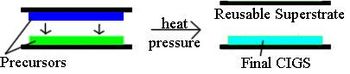 In this process, two different precursor films are deposited separately on a substrate and a superstrate. The films are pressed together and heated to release the film from the superstrate leaving a CIGS absorber on the substrate. This technique allows the superstrate to be reused (Figure 5). Heliovolt
patented this procedure and has named it the FASST process. Therefore, Heliovolt is the only company currently scaling up the technique. In principle, the precursors can be deposited at low temperature using low cost deposition techniques, lowering the final cost of the module. However, the first one or two generations of product will still use higher temperature PVD methods and not achieve full cost cutting potential. Flexible substrates could eventually be used in this process.
Typical film characteristics are not known outside of the company as no research has been conducted by independently funded laboratories. However, Heliovolt has claimed a top cell efficiency of 12.2%.
coevaporation process deposits bilayers of CIGS with different stoichiometries onto a heated substrate and allows them to intermix. The National Renewable Energy Laboratory
(NREL) has developed another process which involves three deposition steps and produced the current CIGS efficiency record holder at 19.9%. The first step in NREL's method is codeposition of In, Ga, and Se. This is followed by Cu and Se deposited at a higher temperature to allow for diffusion and intermixing of the elements. In the final stage In, Ga, and Se are again deposited to make the overall composition Cu deficient.
Würth Solar has been producing CIGS cells using an inline coevaporation system since 2005 with module efficiencies between 11% and 12% by the end of that year. They have subsequently opened another production facility and continued to improve efficiency and yield. Other companies scaling up coevaporation processes include Global Solar
and Ascent Solar
. Global Solar also uses an inline three stage deposition process. In all of the steps Se is supplied in excess in the vapor phase. In and Ga are first evaporated followed by Cu and then by In and Ga to make the film Cu deficient. These films performed quite favorably in relation not only to other manufacturers but also to absorbers grown at NREL and the Institute for Energy Conversion (IEC). However, fully fabricated modules of Global Solar’s films did not perform as well. The property in which the module most obviously under-performed was a low VOC, which is characteristic of high defect density and high recombination velocities. Interestingly, Global Solar’s absorber layer outperformed the NREL absorber in carrier lifetime and hall mobility. However, as completed cells the NREL sample performed better. This is evidence of a poor CIGS/CdS interface, possibly due to the lack of an ODC surface layer on the Global Solar film.
As most of the CIGS research at national laboratories and universities covers coevaporation, companies using this technique stand to gain the most from the scientific community. However, they also face significant disadvantages including uniformity issues over large areas and the related difficulty of coevaporating elements in an inline system. Another disadvantage is high growth temperatures which raise the thermal budget and cost. Additionally, coevaporation is plagued by low material utilization (deposition on chamber walls instead of the substrate, especially for selenium) and expensive vacuum equipment. A way to enhance the utilisation of selenium is the usage of a thermal or plasma-enhanced selenium-cracking process, which can additionally be coupled with an ion beam source
for ion beam assisted deposition
.
(CVD) has been implemented in multiple ways for the deposition of CIGS. Processes include atmosphere pressure metal organic CVD (AP-MOCVD), plasma-enhanced CVD (PECVD), low-pressure MOCVD (LP-MOCVD), and aerosol assisted MOCVD (AA-MOCVD). Current work is focused on changing the typical dual-source precursors to single-source precursors. Multiple source precursors must be homogeneously mixed and the flow rates of the precursors have to be kept at the proper stoichiometry. Single-source precursor methods do not suffer from these drawbacks and should enable better control of film composition compared to multiple source precursors.
CVD is not yet being used by any companies for CIGS synthesis. Currently, CVD produced films have low efficiency and a low VOC, partially a result of a high defect concentration. Additionally, the surfaces of the films are generally quite rough which serves to further decrease the VOC. However, the requisite Cu deficiency has been achieved using AA-MOCVD along with a (112) crystal orientation.
However, if the film quality produced by CVD can be improved, any company using this technique could benefit from knowledge gained in other industries using large area CVD deposition, such as glass coating manufacturers. CVD deposition temperatures are lower than those used for other processes such as co-evaporation and selenization of metallic precursors. Therefore, CVD has a lower thermal budget, reducing the cost. Potential manufacturing problems include difficulties converting CVD to an inline process as well as the expense of handling volatile precursors.
availability issues, the development of the CIGS lags behind CdTe commercially. In the laboratory, 18.7% efficiency on a flexible medium was achieved with CIGS cells., though it remains to be seen how well mass production values can be achieved with any CIGS cell. Commercial production of flexible CIGS cells has begun, in Berlin, Germany, commercial production after initial production runs has begun on an annual 35MW capable facility.
Copper indium gallium selenide
Copper indium gallium selenide is a I-III-VI2 semiconductor material composed of copper, indium, gallium, and selenium. The material is a solid solution of copper indium selenide and copper gallium selenide...
(CuIn1-xGaxSe2 or CIGS) is a direct bandgap semiconductor useful for the manufacture of solar cell
Solar cell
A solar cell is a solid state electrical device that converts the energy of light directly into electricity by the photovoltaic effect....
s. Because the material strongly absorbs sunlight, a much thinner film is required than of other semiconductor materials. The CIGS absorber is deposited on a glass backing, along with electrodes to collect current.
CIGS's absorption coefficient is higher than any other semiconductor used for solar modules. Devices made with CIGS belong to the thin-film category of photovoltaics
Photovoltaics
Photovoltaics is a method of generating electrical power by converting solar radiation into direct current electricity using semiconductors that exhibit the photovoltaic effect. Photovoltaic power generation employs solar panels composed of a number of solar cells containing a photovoltaic material...
(PV). The market for thin-film PV grew at a 60% annual rate from 2002 to 2007 and is still growing rapidly (Figure 1). Therefore, a strong incentive exists to develop and improve deposition methods for these films that will allow lower cost and increased throughput.
Properties
CIGS is a IAlkali metal
The alkali metals are a series of chemical elements in the periodic table. In the modern IUPAC nomenclature, the alkali metals comprise the group 1 elements, along with hydrogen. The alkali metals are lithium , sodium , potassium , rubidium , caesium , and francium...
-III
Group 3 element
The group 3 elements are a group of chemical elements in the periodic table. This group, like other d-block groups, should contain four elements, but it is not agreed what elements belong in the group...
-VI
Group 6 element
A Group 6 element is one in the series of elements in group 6 in the periodic table, which consists of the transition metals chromium , molybdenum , tungsten , and seaborgium ....
2 compound semiconductor material composed of copper
Copper
Copper is a chemical element with the symbol Cu and atomic number 29. It is a ductile metal with very high thermal and electrical conductivity. Pure copper is soft and malleable; an exposed surface has a reddish-orange tarnish...
, indium
Indium
Indium is a chemical element with the symbol In and atomic number 49. This rare, very soft, malleable and easily fusible post-transition metal is chemically similar to gallium and thallium, and shows the intermediate properties between these two...
, gallium
Gallium
Gallium is a chemical element that has the symbol Ga and atomic number 31. Elemental gallium does not occur in nature, but as the gallium salt in trace amounts in bauxite and zinc ores. A soft silvery metallic poor metal, elemental gallium is a brittle solid at low temperatures. As it liquefies...
, and selenium
Selenium
Selenium is a chemical element with atomic number 34, chemical symbol Se, and an atomic mass of 78.96. It is a nonmetal, whose properties are intermediate between those of adjacent chalcogen elements sulfur and tellurium...
. The material is a solid solution
Solid solution
A solid solution is a solid-state solution of one or more solutes in a solvent. Such a mixture is considered a solution rather than a compound when the crystal structure of the solvent remains unchanged by addition of the solutes, and when the mixture remains in a single homogeneous phase...
of copper indium selenide (often abbreviated "CIS") and copper gallium selenide, with a chemical formula of CuInxGa(1-x)Se2, where the value of x can vary from 1 (pure copper indium selenide) to 0 (pure copper gallium selenide). It is a tetrahedrally bond
Chemical bond
A chemical bond is an attraction between atoms that allows the formation of chemical substances that contain two or more atoms. The bond is caused by the electromagnetic force attraction between opposite charges, either between electrons and nuclei, or as the result of a dipole attraction...
ed semiconductor, with the chalcopyrite
Chalcopyrite
Chalcopyrite is a copper iron sulfide mineral that crystallizes in the tetragonal system. It has the chemical composition CuFeS2. It has a brassy to golden yellow color and a hardness of 3.5 to 4 on the Mohs scale. Its streak is diagnostic as green tinged black.On exposure to air, chalcopyrite...
crystal structure. The bandgap varies continuously with x from about 1.0 eV (for copper indium selenide) to about 1.7 eV (for copper gallium selenide).
Thin film solar cell
A thin-film solar cell , also called a thin-film photovoltaic cell , is a solar cell that is made by depositing one or more thin layers of photovoltaic material on a substrate...
.
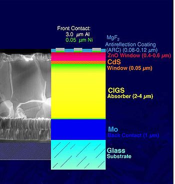
CIGS photovoltaic cells
The most common device structure for CIGS solar cells is shown in Figure 2. Glass is commonly used as a substrate, however, many companies are also looking at lighter and more flexible substrates such as polyimidePolyimide
Polyimide is a polymer of imide monomers. The structure of imide is as shown. Polyimides have been in mass production since 1955...
or metal foils. A molybdenum
Molybdenum
Molybdenum , is a Group 6 chemical element with the symbol Mo and atomic number 42. The name is from Neo-Latin Molybdaenum, from Ancient Greek , meaning lead, itself proposed as a loanword from Anatolian Luvian and Lydian languages, since its ores were confused with lead ores...
layer is deposited (commonly by sputtering
Sputtering
Sputtering is a process whereby atoms are ejected from a solid target material due to bombardment of the target by energetic particles. It is commonly used for thin-film deposition, etching and analytical techniques .-Physics of sputtering:...
) which serves as the back contact and to reflect most unabsorbed light back into the absorber. Following Mo deposition a p-type
P-type semiconductor
A P-type semiconductor is obtained by carrying out a process of doping: that is, adding a certain type of atoms to the semiconductor in order to increase the number of free charge carriers ....
CIGS absorber layer is grown by one of several unique methods. A thin n-type
N-type semiconductor
N-type semiconductors are a type of extrinsic semiconductor where the dopant atoms are capable of providing extra conduction electrons to the host material . This creates an excess of negative electron charge carriers....
buffer layer is added on top of the absorber. The buffer is typically CdS
CDS
-Computing and electronics:* Cadence Design Systems, American Electronic Design Automation software company* Chromatography data system, software to control chromatography instruments* Cockpit display system* Compact Discs...
deposited via chemical bath deposition. The buffer is overlaid with a thin, intrinsic ZnO layer which is capped by a thicker, Al doped ZnO layer. Despite increasing the series resistance, the intrinsic ZnO layer is beneficial to cell performance. The precise mechanism for the improvement is still being debated. The Al doped ZnO serves as a transparent conducting oxide to collect and move electrons out of the cell while absorbing as little light as possible.
The materials based on CuInSe2 that are of interest for photovoltaic applications include several elements from groups I, III and VI in the periodic table. These semiconductors are especially attractive for thin film solar cell application because of their high optical absorption coefficients and versatile optical and electrical characteristics which can in principle be manipulated and tuned for a specific need in a given device.
Conversion efficiency
CIGS is mainly used in the form of polycrystallinePolycrystalline
Polycrystalline materials are solids that are composed of many crystallites of varying size and orientation. The variation in direction can be random or directed, possibly due to growth and processing conditions. Fiber texture is an example of the latter.Almost all common metals, and many ceramics...
thin film
Thin film
A thin film is a layer of material ranging from fractions of a nanometer to several micrometers in thickness. Electronic semiconductor devices and optical coatings are the main applications benefiting from thin film construction....
s. The best efficiency achieved as of December 2005 was 19.5%. A team at the National Renewable Energy Laboratory
National Renewable Energy Laboratory
The National Renewable Energy Laboratory , located in Golden, Colorado, is the United States' primary laboratory for renewable energy and energy efficiency research and development. The National Renewable Energy Laboratory is a government-owned, contractor-operated facility; it is funded through...
achieved 19.9% new world record efficiency by modifying the CIGS surface and making it look like CIS.
These efficiencies are different from module conversion efficiencies. Two of the leading manufacturers of CIGS thin-film PV have hit new record highs in module conversion efficiencies. The U.S. National Renewable Energy Laboratory has confirmed 13.8% efficiency of a large-area (meter-square) production panel, and 13% total-area (and 14.2% aperture-area) efficiency with some production modules.
Higher efficiencies (around 30%) can be obtained by using optics to concentrate
Concentrated photovoltaics
Concentrated photovoltaic technology uses optics such as lenses to concentrate a large amount of sunlight onto a small area of solar photovoltaic materials to generate electricity...
the incident light. The use of gallium increases the optical band gap of the CIGS layer as compared to pure CIS, thus increasing the open-circuit voltage. In another point of view, gallium is added to replace as much indium as possible due to gallium’s relative availability to indium.
Deposition
CIGS films can be manufactured by several different methods:- The most common vacuumVacuumIn everyday usage, vacuum is a volume of space that is essentially empty of matter, such that its gaseous pressure is much less than atmospheric pressure. The word comes from the Latin term for "empty". A perfect vacuum would be one with no particles in it at all, which is impossible to achieve in...
-based process co-evaporates or co-sputters copper, gallium, and indium, then anneals the resulting film with a selenide vapor to form the final CIGS structure. An alternative is to directly co-evaporate copper, gallium, indium and selenium onto a heated substrate. - A non-vacuum-based alternative process deposits nanoparticleNanoparticleIn nanotechnology, a particle is defined as a small object that behaves as a whole unit in terms of its transport and properties. Particles are further classified according to size : in terms of diameter, coarse particles cover a range between 10,000 and 2,500 nanometers. Fine particles are sized...
s of the precursorPrecursor (chemistry)In chemistry, a precursor is a compound that participates in the chemical reaction that produces another compound. In biochemistry, the term "precursor" is used more specifically to refer to a chemical compound preceding another in a metabolic pathway....
materials on the substrate and then sinters them in situ. ElectroplatingElectroplatingElectroplating is a plating process in which metal ions in a solution are moved by an electric field to coat an electrode. The process uses electrical current to reduce cations of a desired material from a solution and coat a conductive object with a thin layer of the material, such as a metal...
is another low cost alternative to apply the CIGS layer.
With record CIGS efficiency at just below 20% for several years, new trends of CIGS research has been focused on lower-cost deposition methods as an alternative to expensive vacuum processes. This new research progressed quickly and efficiencies of 10%–15% have been achieved by many teams.
CIGS and silicon
Unlike the siliconSilicon
Silicon is a chemical element with the symbol Si and atomic number 14. A tetravalent metalloid, it is less reactive than its chemical analog carbon, the nonmetal directly above it in the periodic table, but more reactive than germanium, the metalloid directly below it in the table...
cells based on a homojunction
Homojunction
A homojunction is a semiconductor interface that occurs between layers of similar semiconductor material, these materials have equal band gaps but typically have different doping. In most practical cases a homojunction occurs at the interface between an n-type and p-type semiconductor such as...
, the structure of CIGS cells is a more complex heterojunction
Heterojunction
A heterojunction is the interface that occurs between two layers or regions of dissimilar crystalline semiconductors. These semiconducting materials have unequal band gaps as opposed to a homojunction...
system. CIGS solar cells are not as efficient as crystalline silicon
Monocrystalline silicon
Monocrystalline silicon or single-crystal Si, or mono-Si is the base material of the electronic industry. It consists of silicon in which the crystal lattice of the entire solid is continuous, unbroken to its edges. It can be prepared intrinsic, i.e...
solar cells, for which the record efficiency lies at 24.7%. Though some argue that CIGS will be substantially cheaper due to much lower material costs and potentially lower fabrication costs, in the second quarter of 2011, Veeco, Inc., a company with expertise in thin film deposition technology, closed a major CIGS development project due in part to the continued declining costs of the competing silicon materials and technology.
A direct bandgap material, CIGS has very strong light absorption and only 1–2 micrometers of CIGS is enough to absorb most of the sunlight. A much greater thickness of crystalline silicon is required for the same absorption.
The active layer
Active layer
In environments containing permafrost, the active layer is the top layer of soil that thaws during the summer and freezes again during the autumn. In all climates, whether they contain permafrost or not, the temperature in the lower levels of the soil will remain more stable than that at the...
(CIGS) can be deposited in a polycrystalline
Polycrystalline
Polycrystalline materials are solids that are composed of many crystallites of varying size and orientation. The variation in direction can be random or directed, possibly due to growth and processing conditions. Fiber texture is an example of the latter.Almost all common metals, and many ceramics...
form directly onto molybdenum
Molybdenum
Molybdenum , is a Group 6 chemical element with the symbol Mo and atomic number 42. The name is from Neo-Latin Molybdaenum, from Ancient Greek , meaning lead, itself proposed as a loanword from Anatolian Luvian and Lydian languages, since its ores were confused with lead ores...
coated
Coating
Coating is a covering that is applied to the surface of an object, usually referred to as the substrate. In many cases coatings are applied to improve surface properties of the substrate, such as appearance, adhesion, wetability, corrosion resistance, wear resistance, and scratch resistance...
glass sheets or steel bands. This uses less energy than growing large crystals, which is a necessary step in the manufacture of crystalline silicon solar cells. Also unlike crystalline silicon, these substrates can be flexible
Flexible electronics
Flexible electronics, also known as flex circuits, is a technology for assembling electronic circuits by mounting electronic devices on flexible plastic substrates, such as polyimide, PEEK or transparent conductive polyester film. Additionally, flex circuits can be screen printed silver circuits on...
.
CIGS and other thin films
CIGS belongs in the category of thin film solar cells (TFSC). The semiconductors used as absorber layer in thin-film photovoltaics exhibit direct bandgaps allowing the cells to be a few micrometers thin; hence, the term thin-film solar cells is used. Other materials in this group of TFSC include CdTe and amorphous Si. Their record efficiencies are slightly lower than that of CIGS for lab-scaleLaboratory
A laboratory is a facility that provides controlled conditions in which scientific research, experiments, and measurement may be performed. The title of laboratory is also used for certain other facilities where the processes or equipment used are similar to those in scientific laboratories...
top performance cells. The 19.9% efficiency is by far the highest compared with those achieved by other thin film technologies such as Cadmium Telluride
Cadmium telluride
Cadmium telluride is a crystalline compound formed from cadmium and tellurium. It is used as an infrared optical window and a solar cell material. It is usually sandwiched with cadmium sulfide to form a p-n junction photovoltaic solar cell...
(CdTe) or amorphous silicon
Amorphous silicon
Amorphous silicon is the non-crystalline allotropic form of silicon. It can be deposited in thin films at low temperatures onto a variety of substrates, offering some unique capabilities for a variety of electronics.-Description:...
(a-Si). As for CIS, and CGS solar cells, the world record total area efficiencies are 15.0% and 9.5% respectively. Another advantage of CIGS compared to CdTe is smaller amount of toxic material cadmium are present in CIGS cells.
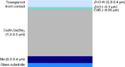
Structure of a CIGS thin-film solar cell
Soda-lime glass
Soda-lime glass, also called soda-lime-silica glass, is the most prevalent type of glass, used for windowpanes, and glass containers for beverages, food, and some commodity items...
of 1–3 mm thickness. This is coated
Coating
Coating is a covering that is applied to the surface of an object, usually referred to as the substrate. In many cases coatings are applied to improve surface properties of the substrate, such as appearance, adhesion, wetability, corrosion resistance, wear resistance, and scratch resistance...
on one side with molybdenum
Molybdenum
Molybdenum , is a Group 6 chemical element with the symbol Mo and atomic number 42. The name is from Neo-Latin Molybdaenum, from Ancient Greek , meaning lead, itself proposed as a loanword from Anatolian Luvian and Lydian languages, since its ores were confused with lead ores...
(Mo) that serves as metal back contact. The heterojunction
Heterojunction
A heterojunction is the interface that occurs between two layers or regions of dissimilar crystalline semiconductors. These semiconducting materials have unequal band gaps as opposed to a homojunction...
is formed between the semiconductors CIGS and ZnO, separated by a thin layer of CdS
CDS
-Computing and electronics:* Cadence Design Systems, American Electronic Design Automation software company* Chromatography data system, software to control chromatography instruments* Cockpit display system* Compact Discs...
and a layer of intrinsic ZnO. The CIGS is doped p-type
P-type semiconductor
A P-type semiconductor is obtained by carrying out a process of doping: that is, adding a certain type of atoms to the semiconductor in order to increase the number of free charge carriers ....
from intrinsic defects, while the ZnO is doped n-type
N-type semiconductor
N-type semiconductors are a type of extrinsic semiconductor where the dopant atoms are capable of providing extra conduction electrons to the host material . This creates an excess of negative electron charge carriers....
to a much larger extent through the incorporation of aluminum (Al). This asymmetric doping causes the space-charge region to extend much further into the CIGS than into the ZnO. Matched to this are the layer thicknesses and the bandgaps of the materials: the wide CIGS layer serves as absorber with a bandgap between 1.02 eV
Electronvolt
In physics, the electron volt is a unit of energy equal to approximately joule . By definition, it is equal to the amount of kinetic energy gained by a single unbound electron when it accelerates through an electric potential difference of one volt...
(CuInSe2) and 1.65 eV (CuGaSe2). Absorption is minimized in the upper layers, called window
Window
A window is a transparent or translucent opening in a wall or door that allows the passage of light and, if not closed or sealed, air and sound. Windows are usually glazed or covered in some other transparent or translucent material like float glass. Windows are held in place by frames, which...
, by the choice of larger bandgaps: Eg,ZnO=3.2 eV and Eg,CdS=2.4 eV. The doped ZnO also serves as front contact for current collection. Laboratory
Laboratory
A laboratory is a facility that provides controlled conditions in which scientific research, experiments, and measurement may be performed. The title of laboratory is also used for certain other facilities where the processes or equipment used are similar to those in scientific laboratories...
scale devices, typically 0.5 cm2 large, are provided with a Ni
Nickel
Nickel is a chemical element with the chemical symbol Ni and atomic number 28. It is a silvery-white lustrous metal with a slight golden tinge. Nickel belongs to the transition metals and is hard and ductile...
/Al
Aluminium
Aluminium or aluminum is a silvery white member of the boron group of chemical elements. It has the symbol Al, and its atomic number is 13. It is not soluble in water under normal circumstances....
-grid deposited
Deposition (chemistry)
In chemistry, deposition is the settling of particles or sediment from a solution, suspension and mixture or vapor onto a pre-existing surface...
onto the front side to contact the ZnO.
Production of modules involves the depositon layer being cut into a series of parallel connected strips. A further transparent protective cover is applied to the module. This sandwich construction is then sealed against the ingress of moisture. Some method of physical support is required to prevent fracture of this fragile structure.
General properties of high performance CIGS absorbers
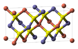
All high performance CIGS absorbers in solar cells have several similarities independent of the growth technique used. First, they are polycrystallinePolycrystalline
Polycrystalline materials are solids that are composed of many crystallites of varying size and orientation. The variation in direction can be random or directed, possibly due to growth and processing conditions. Fiber texture is an example of the latter.Almost all common metals, and many ceramics...
α-phase which has the chalcopyrite
Chalcopyrite
Chalcopyrite is a copper iron sulfide mineral that crystallizes in the tetragonal system. It has the chemical composition CuFeS2. It has a brassy to golden yellow color and a hardness of 3.5 to 4 on the Mohs scale. Its streak is diagnostic as green tinged black.On exposure to air, chalcopyrite...
crystal structure shown in Figure 3. The second property is an overall Cu
Copper
Copper is a chemical element with the symbol Cu and atomic number 29. It is a ductile metal with very high thermal and electrical conductivity. Pure copper is soft and malleable; an exposed surface has a reddish-orange tarnish...
deficiency. Cu deficiency increases the majority carrier (hole) concentration by increasing the number of Cu vacancies. These vacancies act as electron acceptors. Also, when CIGS films are In rich (Cu deficient) the surface layer of the film forms an ordered defect compound (ODC) with a stoichiometry of Cu(In,Ga)3Se5. The ODC is n-type, forming a p-n homojunction in the film at the interface between the α phase and the ODC. Recombination
Carrier generation and recombination
In the solid state physics of semiconductors, carrier generation and recombination are processes by which mobile charge carriers are created and eliminated. Carrier generation and recombination processes are fundamental to the operation of many optoelectronic semiconductor devices, such as...
velocity at the CIGS/CdS interface is decreased by presence of the homojunction. The drop in interface recombination attributable to ODC formation is demonstrated by experiments which have shown recombination in the bulk of the film is the main loss mechanism in Cu deficient films, while in Cu rich films the main loss is at the CIGS/CdS interface.
Sodium (Na) incorporation is also necessary for optimal performance. Ideal Na concentration is considered to be approximately 0.1 at%. Na is commonly supplied by the soda-lime glass
Soda-lime glass
Soda-lime glass, also called soda-lime-silica glass, is the most prevalent type of glass, used for windowpanes, and glass containers for beverages, food, and some commodity items...
used as the substrate, but in processes that do not use this substrate the Na must be deliberately added. Beneficial effects of Na include increases in p-type conductivity, texture
Texture (crystalline)
In materials science, texture is the distribution of crystallographic orientations of a polycrystalline sample. A sample in which these orientations are fully random is said to have no texture. If the crystallographic orientations are not random, but have some preferred orientation, then the...
, and average grain size. Furthermore, Na incorporation allows for performance to be maintained over larger stoichiometric deviations. Simulations have predicted that Na on an In site creates a shallow acceptor level and that Na serves to remove In on Cu defects (donors), but reasons for these benefits are still being debated. Na is also credited with catalyzing oxygen
Oxygen
Oxygen is the element with atomic number 8 and represented by the symbol O. Its name derives from the Greek roots ὀξύς and -γενής , because at the time of naming, it was mistakenly thought that all acids required oxygen in their composition...
absorption. Oxygen passivates Se vacancies that act as compensating donors and recombination centers.
Alloying CIS (CuInSe2) with CGS (CuGaSe2) increases in the bandgap. To reach the ideal bandgap for a single junction solar cell, 1.5 eV, a Ga/(In+Ga) ratio of roughly 0.7 would be optimal. However, at ratios above ~0.3 device performance drops off. Industry currently targets the 0.3 Ga/(In+Ga) ratio, resulting in bandgaps between 1.1 and 1.2 eV. The decreasing performance has been postulated to be a result of CGS not forming the ODC, which is necessary for a good interface with CdS.
The highest efficiency devices show a high degree of texturing, or preferred crystallographic orientation. Until recently record efficiency devices displayed a (112) texture, but now a (204) surface orientation is observed in the best quality devices. A smooth absorber surface is preferred to maximize the ratio of the illuminated area to the area of the interface. The area of the interface increases with roughness while illuminated area remains constant, decreasing open circuit voltage (VOC). Studies have also linked an increase in defect density to decreased VOC. recombination in CIGS has been suggested to be dominated by non-radiative processes. Theoretically, recombination can be controlled by engineering of the film, as opposed to being intrinsic to the material.
Precursor deposition and post processing
Perhaps the most common method used to create CIGS films for commercial use is deposition of precursor materials – always including Cu, In, and Ga, and sometimes including Se – onto a substrate and processing these films at high temperatures under a proper atmosphere. The following sections outline the various techniques for precursor deposition processing, including sputtering of metallic layers at low temperatures, printing of inks containing nanoparticles, electrodepositionElectrophoretic deposition
Electrophoretic deposition , is a term for a broad range of industrial processes which includes electrocoating, e-coating, cathodic electrodeposition, and electrophoretic coating, or electrophoretic painting...
, and a technique inspired by wafer-bonding.
General selenization concerns
The Se supply and selenization environment is extremely important in determining the properties and quality of the film produced from precursor layers. When Se is supplied in the gas phase (for example as H2Se or elemental Se) at high temperatures the Se will become incorporated into the film by absorption and subsequent diffusion. During this step, called chalcogenization, complex interactions occur to form a chalcogenide. These interactions include formation of Cu-In-Ga intermetallic alloys, formation of intermediate metal-selenide binary compounds, and phase separation of various stoichiometric CIGS compounds. Because of the variety and complexity of the reactions taking place, the properties of the CIGS film are difficult to control.Differences exist between films formed using different Se sources. Using H2Se yields the fastest Se incorporation into the absorber; 50 at% Se can be achieved in CIGS films at temperatures as low as 400 °C. By comparison, elemental Se only achieves full incorporation with reaction temperatures of 500 °C and above. Below 500 °C films formed from elemental Se were not only Se deficient, but also had multiple phases including metal selenides and various alloys. Use of H2Se also provides the best compositional uniformity and the largest grain sizes. However, H2Se is highly toxic and is classified as hazardous to the environment.
Sputtering of metallic layers followed by selenization
In this method of forming CIGS absorbers, a metal film of Cu, In, and Ga is sputtered at or near room temperature and reacted in a Se atmosphere at high temperature. This process has higher throughput than coevaporation and compositional uniformity can be more easily achieved.Sputtering a stacked multilayer of metal – for example a Cu/In/Ga/Cu/In/Ga... structure – produces a smoother surface and better crystallinity in the absorber, when compared to a simple bilayer (Cu-Ga alloy/In) or trilayer (Cu/In/Ga) sputtering. These attributes result in higher efficiency devices, but forming the multilayer is a more complicated deposition process and is likely not worth the cost of extra equipment or the added process complexity. Additionally, the reaction rates of Cu/Ga and Cu/In layers with Se are different. If the reaction temperature is not high enough, or not held long enough, CIS and CGS form as separate phases. The same considerations outlined in the previous section apply to Se incorporation.
Companies currently using similar processes include Showa Shell, Avancis(formerly Shell Solar), Miasolé
Miasolé
MiaSolé is a solar energy company developing Copper indium gallium selenide thin-film photovoltaic products. MiaSolé's manufacturing process lays CIGS on a flexible stainless steel substrate...
, Honda Soltec, and Energy Photovoltaics (EPV). Showa Shell sputters a Cu-Ga alloy layer and an In layer, followed by selenization in H2Se and sulfurization in H2S. The sulfurization step appears to passivate the surface in a way similar to CdS in most other cells. Thus, the buffer layer used is Cd-free which eliminates the worries related to the toxicity and environmental impact of Cd. Showa Shell has reported a maximum module efficiency of 13.6% with an average of 11.3% for 3600 cm2 substrates. Shell Solar uses the same technique as Showa Shell to create the absorber; however, they use a CdS layer deposited by chemical vapor deposition. Modules sold by Shell Solar have a specification of 9.4% module efficiency.
Miasole has had great success in procuring venture capital funds for its process and scale up. However, little is known about their sputtering/selenization process beyond their stated efficiency of 9 to 10% for modules.
EPV uses a hybrid between coevaporation and sputtering in which In and Ga are evaporated in a Se atmosphere. This is followed by Cu sputtering and a selenization step. Finally, In and Ga are again evaporated in the presence of Se. Based on Hall measurements, these films have a low carrier concentration and high mobility compared to other devices. EPV films have also been shown to have a low defect concentration.
Chalcogenization of particulate precursor layers
In this method, metal or metal-oxide nanoparticles are used as the precursors for CIGS growth. These nanoparticles are generally suspended in a water based solution and then applied to large areas by various methods, with printing the most common. The film is then dehydrated and, if the precursors are metal-oxides, reduced in a H2/N2 atmosphere. Following dehydration, the remaining porous film is sintered and selenized at temperatures greater than 400 °C.Nanosolar
Nanosolar
Nanosolar is a developer of solar power technology. Based in San Jose, CA, Nanosolar has developed and commercialized a low-cost printable solar cell manufacturing process. The company started selling panels mid-December 2007, and plans to sell them at around $1 per watt...
and International Solar Electric Technology
International Solar Electric Technology
International Solar Electric Technology, or ISET, is a company heavily invested in copper indium gallium selenide photovoltaics. ISET's research...
(ISET) are attempting to scale up this process. ISET uses oxide particles while Nanosolar is extremely secretive about their ink. The ink composition is unknown but there is some implication that Se is also incorporated into Nanosolar's ink. The advantages of this process include uniformity over large areas, non-vacuum or low-vacuum equipment, and adaptability to roll-to-roll manufacturing. When compared to laminar metal precursor layers, the selenization of sintered nanoparticles is more rapid. The increased rate is a result of the greater surface area associated with porosity
Porosity
Porosity or void fraction is a measure of the void spaces in a material, and is a fraction of the volume of voids over the total volume, between 0–1, or as a percentage between 0–100%...
. Decreasing high temperature selenization reduces the thermal budget. Unfortunately, the drawback of porosity is a tendency towards rougher absorber surfaces. Use of particulate precursors allows for printing on a large variety of substrates with high materials utilization, around 90% or more. A disadvantage is that little research and development exists in this area of deposition. In Nanosolar's manufacturing the printed rolls are cut into cells and must be binned and integrated in a fashion similar to how Si devices are made today. The binning process is different from the monolithic integration that many CIGS companies are using. Monolithic integration is far more adaptable to inline production.
Nanosolar has reported a cell (not module) efficiency of 14%, however this has not been verified by any national laboratory testing, nor are they allowing any onsite inspections of their facilities to verify this and other claims made in the past. In independent testing ISET's absorber had the 2nd lowest efficiency at 8.6%. However, all the modules that beat ISET's module were coevaporated, a process which has manufacturing disadvantages and higher costs. ISET's sample suffered most from low VOC and low fill factor, indicative of a rough surface and/or a high number of defects aiding recombination. Related to these issues, the film had poor transport properties including a low Hall mobility and short carrier lifetime.
Electrodeposition followed by selenization
Precursors can also be deposited by electrodeposition. Two different methodologies exist: deposition of elemental layered structures, and simultaneous deposition of all elements (including Se). Both methods require thermal treatment in a Se atmosphere to make device quality films. Because electrodeposition requires conductive electrodes, metal foils are a logical substrate. Electrodeposition of elemental layers is similar to the sputtering of elemental layers. Currently no company is scaling up this process.Simultaneous deposition is performed using a working electrode (cathode
Cathode
A cathode is an electrode through which electric current flows out of a polarized electrical device. Mnemonic: CCD .Cathode polarity is not always negative...
), a counter electrode (anode
Anode
An anode is an electrode through which electric current flows into a polarized electrical device. Mnemonic: ACID ....
), and a reference electrode as in Figure 4. A metal foil substrate is used as the working electrode in industrial processes. An inert material is used for the counter electrode, and the reference electrode exists to measure and control the potential difference between the anode and cathode. The reference electrode allows the process to be performed potentiostatically, meaning the potential of the substrate can be controlled.
Electrodeposition of all elements simultaneously is a difficult processing problem for a variety of reasons. First, the standard reduction potentials of the elements are not the same, causing preferential deposition of a single element. This problem is commonly alleviated by adding different counter ions into solution for each ion to be deposited (Cu2+, Se4+, In3+, and Ga3+), thus changing the reduction potential for that ion. Second, the Cu-Se system has a complicated behavior and the composition of the film depends on the Se4+/Cu2+ ion flux ratio which can vary over the film surface. Because of this behavior the deposition conditions, specifically precursor concentrations and deposition potential, need to be optimized. Even with optimization, reproducibility is low over large areas due to composition variations and potential drops along the substrate.
The resulting films have small grains, are Cu-rich, and generally contain Cu2-xSex phases along with impurities from the solution. Annealing
Annealing (metallurgy)
Annealing, in metallurgy and materials science, is a heat treatment wherein a material is altered, causing changes in its properties such as strength and hardness. It is a process that produces conditions by heating to above the recrystallization temperature, maintaining a suitable temperature, and...
is required to improve crystallinity. In order to achieve efficiencies higher than 7%, a stoichiometry correction is also required. The correction is done via high temperature physical vapor deposition which is not practical in industry.
Having solved the optimization issues, Solopower is currently producing cells with >13.7% conversion efficiency as per NREL. SoloPower is currently attempting to scale up the process, but few details have been released. SoloPower is relying on the advantages of roll-to-roll manufacturing and flexible metal foil substrates.
Precursor combination by wafer-bonding inspired technique
HelioVolt
HelioVolt Corporation is a privately held U.S. energy company in the solar energy sector. It manufactures photovoltaic solar modules using a thin film semiconductor process based on Copper Indium Gallium Selenide to produce photovoltaic modules...
patented this procedure and has named it the FASST process. Therefore, Heliovolt is the only company currently scaling up the technique. In principle, the precursors can be deposited at low temperature using low cost deposition techniques, lowering the final cost of the module. However, the first one or two generations of product will still use higher temperature PVD methods and not achieve full cost cutting potential. Flexible substrates could eventually be used in this process.
Typical film characteristics are not known outside of the company as no research has been conducted by independently funded laboratories. However, Heliovolt has claimed a top cell efficiency of 12.2%.
Coevaporation
Coevaporation, or codeposition, is the most prevalent CIGS fabrication technique in the laboratory and an important method in industry. The BoeingBoeing
The Boeing Company is an American multinational aerospace and defense corporation, founded in 1916 by William E. Boeing in Seattle, Washington. Boeing has expanded over the years, merging with McDonnell Douglas in 1997. Boeing Corporate headquarters has been in Chicago, Illinois since 2001...
coevaporation process deposits bilayers of CIGS with different stoichiometries onto a heated substrate and allows them to intermix. The National Renewable Energy Laboratory
National Renewable Energy Laboratory
The National Renewable Energy Laboratory , located in Golden, Colorado, is the United States' primary laboratory for renewable energy and energy efficiency research and development. The National Renewable Energy Laboratory is a government-owned, contractor-operated facility; it is funded through...
(NREL) has developed another process which involves three deposition steps and produced the current CIGS efficiency record holder at 19.9%. The first step in NREL's method is codeposition of In, Ga, and Se. This is followed by Cu and Se deposited at a higher temperature to allow for diffusion and intermixing of the elements. In the final stage In, Ga, and Se are again deposited to make the overall composition Cu deficient.
Würth Solar has been producing CIGS cells using an inline coevaporation system since 2005 with module efficiencies between 11% and 12% by the end of that year. They have subsequently opened another production facility and continued to improve efficiency and yield. Other companies scaling up coevaporation processes include Global Solar
Global Solar
Global Solar Energy is a manufacturer of copper indium gallium diselenide thin-film solar cells, with manufacturing operations in Tucson, Arizona, USA, and Berlin, Germany.- Technology :...
and Ascent Solar
Ascent Solar
Ascent Solar Technologies, Inc. is a publicly traded solar energy company located in Littleton Colorado. Its primary product is a flexible thin film photovoltaic material on a plastic substrate...
. Global Solar also uses an inline three stage deposition process. In all of the steps Se is supplied in excess in the vapor phase. In and Ga are first evaporated followed by Cu and then by In and Ga to make the film Cu deficient. These films performed quite favorably in relation not only to other manufacturers but also to absorbers grown at NREL and the Institute for Energy Conversion (IEC). However, fully fabricated modules of Global Solar’s films did not perform as well. The property in which the module most obviously under-performed was a low VOC, which is characteristic of high defect density and high recombination velocities. Interestingly, Global Solar’s absorber layer outperformed the NREL absorber in carrier lifetime and hall mobility. However, as completed cells the NREL sample performed better. This is evidence of a poor CIGS/CdS interface, possibly due to the lack of an ODC surface layer on the Global Solar film.
As most of the CIGS research at national laboratories and universities covers coevaporation, companies using this technique stand to gain the most from the scientific community. However, they also face significant disadvantages including uniformity issues over large areas and the related difficulty of coevaporating elements in an inline system. Another disadvantage is high growth temperatures which raise the thermal budget and cost. Additionally, coevaporation is plagued by low material utilization (deposition on chamber walls instead of the substrate, especially for selenium) and expensive vacuum equipment. A way to enhance the utilisation of selenium is the usage of a thermal or plasma-enhanced selenium-cracking process, which can additionally be coupled with an ion beam source
Ion beam
An ion beam is a type of charged particle beam consisting of ions. Ion beams have many uses in electronics manufacturing and other industries. A variety of ion beam sources exist, some derived from the mercury vapor thrusters developed by NASA in the 1960s.-Ion beam etching or sputtering:One type...
for ion beam assisted deposition
Ion beam assisted deposition
Ion beam assisted deposition or IBAD or ""IAD"" is a materials engineering technique which combines ion implantation with simultaneous sputtering or another physical vapor deposition technique...
.
Chemical vapor deposition
Chemical vapor depositionChemical vapor deposition
Chemical vapor deposition is a chemical process used to produce high-purity, high-performance solid materials. The process is often used in the semiconductor industry to produce thin films. In a typical CVD process, the wafer is exposed to one or more volatile precursors, which react and/or...
(CVD) has been implemented in multiple ways for the deposition of CIGS. Processes include atmosphere pressure metal organic CVD (AP-MOCVD), plasma-enhanced CVD (PECVD), low-pressure MOCVD (LP-MOCVD), and aerosol assisted MOCVD (AA-MOCVD). Current work is focused on changing the typical dual-source precursors to single-source precursors. Multiple source precursors must be homogeneously mixed and the flow rates of the precursors have to be kept at the proper stoichiometry. Single-source precursor methods do not suffer from these drawbacks and should enable better control of film composition compared to multiple source precursors.
CVD is not yet being used by any companies for CIGS synthesis. Currently, CVD produced films have low efficiency and a low VOC, partially a result of a high defect concentration. Additionally, the surfaces of the films are generally quite rough which serves to further decrease the VOC. However, the requisite Cu deficiency has been achieved using AA-MOCVD along with a (112) crystal orientation.
However, if the film quality produced by CVD can be improved, any company using this technique could benefit from knowledge gained in other industries using large area CVD deposition, such as glass coating manufacturers. CVD deposition temperatures are lower than those used for other processes such as co-evaporation and selenization of metallic precursors. Therefore, CVD has a lower thermal budget, reducing the cost. Potential manufacturing problems include difficulties converting CVD to an inline process as well as the expense of handling volatile precursors.
Electrospray Deposition
Recently, a new techinique for the deposition of CIS films have been introduced known as Electrospray deposition. The technique involves the electric field assisted spray of ink containing CIS nano-particles onto the substrate directly and then sintering in inert environment. The main advantage of this technique is that the process takes place at room conditions and it is possible to attach this process with some contnous or mass production system like roll-to-roll production mechanism.Breakthroughs and Commercial
Despite CIGS having the advantage over CdTe where both heavy metal Cadmium usage as well as rare-earth TellurideTelluride (chemistry)
The telluride ion is Te2−. It is the final stable member of the series of dianions O2−, S2−, and Se2− ....
availability issues, the development of the CIGS lags behind CdTe commercially. In the laboratory, 18.7% efficiency on a flexible medium was achieved with CIGS cells., though it remains to be seen how well mass production values can be achieved with any CIGS cell. Commercial production of flexible CIGS cells has begun, in Berlin, Germany, commercial production after initial production runs has begun on an annual 35MW capable facility.
External links
- Copper Indium Diselenide Publications, Presentations, and News Database of the National Renewable Energy LaboratoryNational Renewable Energy LaboratoryThe National Renewable Energy Laboratory , located in Golden, Colorado, is the United States' primary laboratory for renewable energy and energy efficiency research and development. The National Renewable Energy Laboratory is a government-owned, contractor-operated facility; it is funded through...
. - World's Largest CIGS Solar Array Operational In Arizona.
- Michael Kanellos Silicon vs. CIGS: With solar energy, the issue is material October 2, 2006 CNET News.com
- CIGS to emerge as the major thin-film photovoltaic technology by 2020