

Transparent conducting film
Encyclopedia
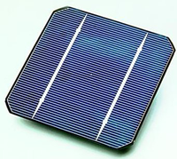
Transparent conducting films (TCFs) are optically transparent and electrically conductive in thin layers.
TCFs for photovoltaic applications have been fabricated from both inorganic and organic materials. Inorganic films typically are made up of a layer of TCO (transparent conducting oxide), generally in the form of indium tin oxide
(ITO), fluorine doped tin oxide (FTO), and doped zinc oxide
. Organic films are being developed using carbon nanotube
networks and graphene
, which can be fabricated to be highly transparent to the infrared light, along with networks of polymers such as poly(3,4-ethylenedioxythiophene)
and its derivatives.
Transparent conducting films act, as a window for light to pass through to the active material beneath (where carrier generation occurs), as an ohmic contact for carrier transport out of the photovoltaic but also as transparent carrier for smd electronics
used between laminated glass
or light transmissive composites
. Transparent materials possess bandgaps with energies corresponding to wavelengths which are shorter than the visible range of 380 nm to 750 nm. As such, photons with energies below the bandgap are not collected by these materials and thus visible light passes through. However, applications such as photovoltaics may require an even broader bandgap to avoid unwanted absorption of the solar spectra.
| |}>
or amorphous microstructures. On average, these applications use electrode materials that have greater than 80% transmittance of incident light as well as conductivities higher than 103 S
/cm for efficient carrier transport. The transmittance of these films, just as in any transparent material, is limited by light scattering at defects and grain boundaries. In general, TCOs for use as thin-film electrodes in solar cells should have a minimum carrier concentration on the order of 1020 cm−3 for low resistivity and a bandgap greater than 380 nm to avoid absorption of light over most of the solar spectra. Mobility in these films is limited by ionized impurity scattering and is on the order of 40 cm2/(V·s). Current transparent conducting oxides used in industry are primarily n-type conductors, meaning their primary conduction is from the flow of electrons. Suitable p-type transparent conducting oxides are still being researched.
To date, the industry standard in TCO is ITO, or tin-doped indium-oxide
. This material boasts a low resistivity of ~10−4 Ω·cm and a transmittance of greater than 80%. However ITO has the drawback of being expensive. Indium
, the film’s primary metal, is rare (6000 metric tons worldwide in 2006), and its price fluctuates due to market demand (over $800 per kg in 2006). For this reason, doped binary compounds such as aluminum-doped zinc-oxide (AZO) and indium-doped cadmium-oxide
have been proposed as alternative materials. AZO is composed of aluminum and zinc, two common and inexpensive materials, while indium-doped cadmium oxide only uses indium in low concentrations.
Binary compounds of metal oxides without any intentional impurity doping have also been developed for use as TCOs. These systems are typically n-type with a carrier concentration on the order of 1020 cm−3, provided by interstitial metal ions and oxygen vacancies which both act as donors. However, these simple TCOs have not found practical use due to their electrical properties’ high temperature and oxygen partial pressure dependence.
substrate. This glass substrate, apart from providing a support that the oxide can grow on, has the additional benefit of blocking most infrared wavelengths greater than 2 µm for most silicates, and converting it to heat in the glass layer. This in turn helps maintain a low temperature of the active region of the solar cell, which degrades in performance as it heats up. TCO films can be deposited on a substrate through various deposition methods, including metal organic chemical vapor deposition
(MOCVD), metal organic molecular beam deposition (MOMBD), spray pyrolysis, and pulsed laser deposition
(PLD), however conventional fabrication techniques typically involve magnetron sputtering
of the film. The sputtering process is very inefficient, with only 30% of the material actually being deposited on the substrate. In the case of ITO this inefficiency is a significant drawback, however work is still underway to increase the recoverable amount of the unused material. Growth typically is performed in a reducing environment to encourage oxygen vacancy formation within the film, which contribute to the carrier concentration (if n-type).
Here “O” in the subscripts indicates that both the initially bonded oxygen and the vacancy that is produced lie on an oxygen lattice site, while the superscripts on the oxygen and vacancy indicate charge. Thus to enhance their electrical properties, ITO films and other transparent conducting oxides are grown in reducing environments, which encourage oxygen vacancy formation.
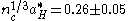
Dopant ionization within the oxide occurs in the same way as in other semiconductor crystals. Shallow donors near the conduction band (n-type) allow electrons to be thermally excited into the conduction band, while acceptors near the valence band (p-type) allow electrons to jump from the valence band to the acceptor level, populating the valence band with holes. It is important to note that carrier scattering in these oxides arises primarily from ionized impurity scattering. Charged impurity ions and point defects have scattering cross-sections that are much greater than their neutral counterparts. Increasing the scattering decreases the mean-free path of the carriers in the oxide, which leads to poor device performance and a high resistivity. These materials can be modeled reasonably well by the free electron gas theory assuming a parabolic conduction band and doping levels above the Mott Criterion. This criterion states that an insulator such as an oxide can experience a composition-induced transition to a metallic state given a minimum doping concentration nc, determined by:
where aH* is the mean ground state Bohr radius
. For ITO, this value requires a minimum doping concentration of roughly 1019 cm−3. Above this level, the typically electrically insulating material becomes metallic and is capable of allowing carrier flow.
s were reported in the mid the 20th century as derivatives of polyaniline. Research continued on such polymers in the 1960s and 70s and continued into the turn of the 21st century. Most conductive polymers are derivatives of polyacetylene
, polyaniline
, polypyrrole
or polythiophene
s. These polymers have conjugated double bonds
which allow for conduction. By manipulating the band structure, polythiophenes have been modified to achieve a HOMO-LUMO
separation (bandgap) that is large enough to make them transparent to visible light.
The transparent conductive polymers can be made into flexible films making them desirable despite their lower conductivity. This makes them useful in the development of flexible electronics
where traditional transparent conductors will fail.
(PEDOT) has conductivity of up to around 1,000 S/cm. Thin oxidized PEDOT films have approx. 10% or less absorption in the visible spectrum and excellent stability. However, PEDOT is insoluble in water making processing more difficult and costly.
The bandgap of PEDOT can be varied between 1.4 and 2.5 eV by varying the degree of π-overlap along the backbone. This can be done by adding substituents along the chain, which result in steric interactions preventing π-overlap. Substituents can also be electron-accepting or donating which will modify the electronic character and thus modify the bandgap. This allows for the formation of a wide bandgap conductor which is transparent to the visible spectrum.
PEDOT is prepared by mixing EDT monomer with an oxidizing agent such as FeCl3
. The oxidizing agent acts as an initiator for polymerization. Research has shown that increasing the ratio of [FeCl3]/[monomer] decreases the solubility of the PEDOT. This is thought to be a result of increased crosslinking
in the polymer making it more difficult to dissolve in a solvent.
is water soluble making processing easier. PEDOT:PSS has a conductivity ranging from 400 to 600 S/cm while still transmitting ~80% of visible light. Treatment in air at 100 °C for over 1000 hours will result in a minimal change in conductivity.
PEDOT:PSS is prepared by polymerizing EDT monomer in an aqueous solution of PSS using Na2S2O8 as the oxidizing agent. This aqueous solution is then spin coated and dried to make a film.
or 2,3-dichloro-5,6-dicyano-1,4-benzoquinone
(DDQ) to form a transparent conductor. The doped polymer has low absorption of the visible spectrum with an absorption band centered around 1050 nm. When doped with iodine, a conductivity of 0.35 S/cm can be achieved. However, the iodine has a tendency to diffuse out in air, making the iodine-doped poly(4,4-dioctylcyclopentadithiophene) unstable.
DDQ itself has a conductivity of 1.1 S/cm. However, DDQ-doped poly(4,4-dioctylcyclopentadithiophene) also tends to decrease its conductivity in air. DDQ-doped polymer has better stability than the iodine-doped polymer, but the stability is still below that of PEDOT. In summary, poly(4,4-dioctylcyclopentadithiophene) has inferior properties relative to PEDOT and PEDOT:PSS, which need to be improved for realistic applications.
Poly(4,4-dioctylcyclopentadithiophene) is solution polymerized by combining monomer with iron(III) chloride
. Once the polymerization is complete the doping is done by exposing the polymer to iodine vapor or DDQ solution.
Carbon nanotubes (CNTs) have attracted much attention because of their materials properties, including a high elastic modulus (~1–2 TPa), a high tensile strength (~13–53 GPa), and a high conductivity (metallic tubes can theoretically carry an electrical current density of 4×10⁹ A/cm2, which is ~1000 times higher than for other metals such as copper
). CNT thin films have been used as transparent electrodes in TCFs because of these good electronic properties.
, electric-arc discharge, or different forms of chemical vapor deposition
(such as PECVD). However, nanotubes are grown en-masse, with nanotubes of different chiralities stuck together due to van der Waals attraction
. Density gradient ultracentrifugation (DGU) has recently been used to get rid of this problem. Using DGU, transparent conductors were constructed using only metallic tubes. Because DGU allows for separation by density, tubes with similar optical properties (due to similar diameters) were selected and used to make CNT conductive films of different colors.
In order to separate the grown tubes, the CNTs are mixed with surfactant and water and sonicated until satisfactory separation occurs. This solution is then sprayed onto the desired substrate in order to create a CNT thin film. The film is then rinsed in water in order to get rid of excess surfactant.
(ITO). PV devices made with these TCOs attained energy-conversion efficiencies of 19.5% in CuIn1−xGaxSe2-based (CIGS
) solar cells and 16.5% in CdTe
-based solar cells. These photovoltaic devices had much higher efficiencies compared to the devices made with CNT thin films: Britz et al. report an efficiency of 8%, with an open circuit voltage (Voc) of 0.676 V, a short circuit flux (Jsc) of 23.9 mA/cm2, and a fill factor of 45.48%. However, CNT thin films show many advantages over other transparent electrodes in the IR range. CNT thin films were reported to have a transmittance of over 90% in this range (400 nm – 22 µm). This paves the way for new applications, indicating that CNT thin films can be used as heat dissipaters in solar cells because of this high transmittance.
As stated previously, nanotube chirality is important in helping determine its potential aid to these devices. Before mass production can occur, more research is needed in exploring the significance of tube diameter and chirality for transparent conducting films in photovoltaic applications. It is expected that the conductivity of the SWNT thin films will increase with an increase in CNT length and purity. As stated previously, the CNT films are made using randomly oriented bundles of CNTs. Ordering these tubes should also increase conductivity, as it will minimize scattering losses and improve contact between the nanotubes.
TCFs for photovoltaic applications have been fabricated from both inorganic and organic materials. Inorganic films typically are made up of a layer of TCO (transparent conducting oxide), generally in the form of indium tin oxide
Indium tin oxide
Indium tin oxide is a solid solution of indium oxide and tin oxide , typically 90% In2O3, 10% SnO2 by weight. It is transparent and colorless in thin layers while in bulk form it is yellowish to grey...
(ITO), fluorine doped tin oxide (FTO), and doped zinc oxide
Zinc oxide
Zinc oxide is an inorganic compound with the formula ZnO. It is a white powder that is insoluble in water. The powder is widely used as an additive into numerous materials and products including plastics, ceramics, glass, cement, rubber , lubricants, paints, ointments, adhesives, sealants,...
. Organic films are being developed using carbon nanotube
Carbon nanotube
Carbon nanotubes are allotropes of carbon with a cylindrical nanostructure. Nanotubes have been constructed with length-to-diameter ratio of up to 132,000,000:1, significantly larger than for any other material...
networks and graphene
Graphene
Graphene is an allotrope of carbon, whose structure is one-atom-thick planar sheets of sp2-bonded carbon atoms that are densely packed in a honeycomb crystal lattice. The term graphene was coined as a combination of graphite and the suffix -ene by Hanns-Peter Boehm, who described single-layer...
, which can be fabricated to be highly transparent to the infrared light, along with networks of polymers such as poly(3,4-ethylenedioxythiophene)
Poly(3,4-ethylenedioxythiophene)
Poly or PEDOT is a conducting polymer based on 3,4-ethylenedioxylthiophene or EDOT monomer. Advantages of this polymer are optical transparency in its conducting state, high stability and moderate band gap and low redox potential...
and its derivatives.
Transparent conducting films act, as a window for light to pass through to the active material beneath (where carrier generation occurs), as an ohmic contact for carrier transport out of the photovoltaic but also as transparent carrier for smd electronics
LEDFilm
The LED Film, also called LED embedded film or LED lighting film is a thin and flexible electronic circuit with surface mounted light emitting diodes on the polymeric film...
used between laminated glass
Ledglass
Ledglass is a building material which contains some functional electronics, light-emitting diodes. The LEDGlass and its technology is described in different articles, It allows for example glass facades to be used as marketing area or windshield glasses to be used as display...
or light transmissive composites
LED Headliner
The Dictionary of Automotive Terms defines headliners "as fabric or vinyl upholstery on the interior of the roof of a vehicle". Wikipedia's definition is a bit more informative: "A headliner is a composite material that consists of a face fabric with nonwoven or foam backing that is adhered to the...
. Transparent materials possess bandgaps with energies corresponding to wavelengths which are shorter than the visible range of 380 nm to 750 nm. As such, photons with energies below the bandgap are not collected by these materials and thus visible light passes through. However, applications such as photovoltaics may require an even broader bandgap to avoid unwanted absorption of the solar spectra.
Transparent conducting oxides
Overview
Transparent conductive oxides (TCO) are doped metal oxides used in optoelectronic devices such as flat panel displays and photovoltaics (including inorganic devices, organic devices, and dye-sensitized solar cell). Most of these films are fabricated with polycrystallinePolycrystalline
Polycrystalline materials are solids that are composed of many crystallites of varying size and orientation. The variation in direction can be random or directed, possibly due to growth and processing conditions. Fiber texture is an example of the latter.Almost all common metals, and many ceramics...
or amorphous microstructures. On average, these applications use electrode materials that have greater than 80% transmittance of incident light as well as conductivities higher than 103 S
Siemens (unit)
The siemens is the SI derived unit of electric conductance and electric admittance. Conductance and admittance are the reciprocals of resistance and impedance respectively, hence one siemens is equal to the reciprocal of one ohm, and is sometimes referred to as the mho. In English, the term...
/cm for efficient carrier transport. The transmittance of these films, just as in any transparent material, is limited by light scattering at defects and grain boundaries. In general, TCOs for use as thin-film electrodes in solar cells should have a minimum carrier concentration on the order of 1020 cm−3 for low resistivity and a bandgap greater than 380 nm to avoid absorption of light over most of the solar spectra. Mobility in these films is limited by ionized impurity scattering and is on the order of 40 cm2/(V·s). Current transparent conducting oxides used in industry are primarily n-type conductors, meaning their primary conduction is from the flow of electrons. Suitable p-type transparent conducting oxides are still being researched.
To date, the industry standard in TCO is ITO, or tin-doped indium-oxide
Indium tin oxide
Indium tin oxide is a solid solution of indium oxide and tin oxide , typically 90% In2O3, 10% SnO2 by weight. It is transparent and colorless in thin layers while in bulk form it is yellowish to grey...
. This material boasts a low resistivity of ~10−4 Ω·cm and a transmittance of greater than 80%. However ITO has the drawback of being expensive. Indium
Indium
Indium is a chemical element with the symbol In and atomic number 49. This rare, very soft, malleable and easily fusible post-transition metal is chemically similar to gallium and thallium, and shows the intermediate properties between these two...
, the film’s primary metal, is rare (6000 metric tons worldwide in 2006), and its price fluctuates due to market demand (over $800 per kg in 2006). For this reason, doped binary compounds such as aluminum-doped zinc-oxide (AZO) and indium-doped cadmium-oxide
Cadmium oxide
Cadmium oxide is an inorganic compound with the formula CdO. It is one of the main precursors to other cadmium compounds. It crystallizes in a cubic rocksalt lattice like sodium chloride, with octahedral cation and anion centers. It occurs naturally as the rare mineral monteponite. Cadmium oxide...
have been proposed as alternative materials. AZO is composed of aluminum and zinc, two common and inexpensive materials, while indium-doped cadmium oxide only uses indium in low concentrations.
Binary compounds of metal oxides without any intentional impurity doping have also been developed for use as TCOs. These systems are typically n-type with a carrier concentration on the order of 1020 cm−3, provided by interstitial metal ions and oxygen vacancies which both act as donors. However, these simple TCOs have not found practical use due to their electrical properties’ high temperature and oxygen partial pressure dependence.
Fabrication
Doped metal oxides for use as transparent conducting layers in photovoltaic devices are typically grown on a glassGlass
Glass is an amorphous solid material. Glasses are typically brittle and optically transparent.The most familiar type of glass, used for centuries in windows and drinking vessels, is soda-lime glass, composed of about 75% silica plus Na2O, CaO, and several minor additives...
substrate. This glass substrate, apart from providing a support that the oxide can grow on, has the additional benefit of blocking most infrared wavelengths greater than 2 µm for most silicates, and converting it to heat in the glass layer. This in turn helps maintain a low temperature of the active region of the solar cell, which degrades in performance as it heats up. TCO films can be deposited on a substrate through various deposition methods, including metal organic chemical vapor deposition
Metalorganic vapour phase epitaxy
Metalorganic vapour phase epitaxy , also known as organometallic vapour phase epitaxy or metalorganic chemical vapour deposition , is a chemical vapour deposition method of epitaxial growth of materials, especially compound semiconductors, from the surface reaction of organic compounds or...
(MOCVD), metal organic molecular beam deposition (MOMBD), spray pyrolysis, and pulsed laser deposition
Pulsed laser deposition
Pulsed laser deposition is a thin film deposition technique where a high power pulsed laser beam is focused inside a vacuum chamber to strike a target of the material that is to be deposited...
(PLD), however conventional fabrication techniques typically involve magnetron sputtering
Sputtering
Sputtering is a process whereby atoms are ejected from a solid target material due to bombardment of the target by energetic particles. It is commonly used for thin-film deposition, etching and analytical techniques .-Physics of sputtering:...
of the film. The sputtering process is very inefficient, with only 30% of the material actually being deposited on the substrate. In the case of ITO this inefficiency is a significant drawback, however work is still underway to increase the recoverable amount of the unused material. Growth typically is performed in a reducing environment to encourage oxygen vacancy formation within the film, which contribute to the carrier concentration (if n-type).
Theory
Charge carriers in these oxides arise from three fundamental sources: interstitial metal ion impurities, oxygen vacancies, and doping ions. The first two sources always act as electron donors. Indeed some TCOs are fabricated solely using these two intrinsic sources as carrier generators. When an oxygen vacancy is present in the lattice it acts as a doubly charged electron donor. In ITO, for example, each oxygen vacancy causes the neighboring In3+ ion 5s orbitals to be stabilized from the 5s conduction band by the missing bonds to the oxygen ion, while two electrons are trapped at the site due to charge neutrality effects. This stabilization of the 5s orbitals causes a formation of a donor level for the oxygen ion, determined to be 0.03 eV below the conduction band. Thus these defects act as shallow donors to the bulk crystal. Common notation for this doping is Kröger–Vink notation and is written as:
Here “O” in the subscripts indicates that both the initially bonded oxygen and the vacancy that is produced lie on an oxygen lattice site, while the superscripts on the oxygen and vacancy indicate charge. Thus to enhance their electrical properties, ITO films and other transparent conducting oxides are grown in reducing environments, which encourage oxygen vacancy formation.
Dopant ionization within the oxide occurs in the same way as in other semiconductor crystals. Shallow donors near the conduction band (n-type) allow electrons to be thermally excited into the conduction band, while acceptors near the valence band (p-type) allow electrons to jump from the valence band to the acceptor level, populating the valence band with holes. It is important to note that carrier scattering in these oxides arises primarily from ionized impurity scattering. Charged impurity ions and point defects have scattering cross-sections that are much greater than their neutral counterparts. Increasing the scattering decreases the mean-free path of the carriers in the oxide, which leads to poor device performance and a high resistivity. These materials can be modeled reasonably well by the free electron gas theory assuming a parabolic conduction band and doping levels above the Mott Criterion. This criterion states that an insulator such as an oxide can experience a composition-induced transition to a metallic state given a minimum doping concentration nc, determined by:
where aH* is the mean ground state Bohr radius
Bohr radius
The Bohr radius is a physical constant, approximately equal to the most probable distance between the proton and electron in a hydrogen atom in its ground state. It is named after Niels Bohr, due to its role in the Bohr model of an atom...
. For ITO, this value requires a minimum doping concentration of roughly 1019 cm−3. Above this level, the typically electrically insulating material becomes metallic and is capable of allowing carrier flow.
Transparent conducting polymers
Conductive polymerConductive polymer
Conductive polymers or, more precisely, intrinsically conducting polymers are organic polymers that conduct electricity. Such compounds may have metallic conductivity or can be semiconductors. The biggest advantage of conductive polymers is their processability, mainly by dispersion. Conductive...
s were reported in the mid the 20th century as derivatives of polyaniline. Research continued on such polymers in the 1960s and 70s and continued into the turn of the 21st century. Most conductive polymers are derivatives of polyacetylene
Polyacetylene
Polyacetylene is an organic polymer with the repeat unit n. The high electrical conductivity discovered for these polymers beginning in the 1960's accelerated interest in the use of organic compounds in microelectronics...
, polyaniline
Polyaniline
Polyaniline is a conducting polymer of the semi-flexible rod polymer family. Although the compound itself was discovered over 150 years ago, only since the early 1980s has polyaniline captured the intense attention of the scientific community. This is due to the rediscovery of its high electrical...
, polypyrrole
Polypyrrole
Polypyrrole is a chemical compound formed from a number of connected pyrrole ring structures. For example a tetrapyrrole is a compound with four pyrrole rings connected. Methine-bridged cyclic tetrapyrroles are called porphyrins. Polypyrroles are conducting polymers of the rigid-rod polymer host...
or polythiophene
Polythiophene
Polythiophenes result from the polymerization of thiophenes, a sulfur heterocycle, that can become conducting when electrons are added or removed from the conjugated π-orbitals via doping....
s. These polymers have conjugated double bonds
Conjugated system
In chemistry, a conjugated system is a system of connected p-orbitals with delocalized electrons in compounds with alternating single and multiple bonds, which in general may lower the overall energy of the molecule and increase stability. Lone pairs, radicals or carbenium ions may be part of the...
which allow for conduction. By manipulating the band structure, polythiophenes have been modified to achieve a HOMO-LUMO
HOMO/LUMO
HOMO and LUMO are acronyms for highest occupied molecular orbital and lowest unoccupied molecular orbital, respectively. The energy difference between the HOMO and LUMO is termed the HOMO-LUMO gap...
separation (bandgap) that is large enough to make them transparent to visible light.
Applications
Transparent conductive polymers can be [are?] used as electrodes on light emitting diodes and photovoltaic devices. They have conductivity below that of transparent conducting oxides but have low absorption of the visible spectrum allowing them to act as a transparent conductor on these devices. However, because transparent conductive polymers do absorb some of the visible spectrum and significant amounts of the mid to near IR, they lower the efficiency of photovoltaic devices.The transparent conductive polymers can be made into flexible films making them desirable despite their lower conductivity. This makes them useful in the development of flexible electronics
Flexible electronics
Flexible electronics, also known as flex circuits, is a technology for assembling electronic circuits by mounting electronic devices on flexible plastic substrates, such as polyimide, PEEK or transparent conductive polyester film. Additionally, flex circuits can be screen printed silver circuits on...
where traditional transparent conductors will fail.
Poly(3,4-ethylenedioxythiophene) (PEDOT)
Poly(3,4-ethylenedioxythiophene)Poly(3,4-ethylenedioxythiophene)
Poly or PEDOT is a conducting polymer based on 3,4-ethylenedioxylthiophene or EDOT monomer. Advantages of this polymer are optical transparency in its conducting state, high stability and moderate band gap and low redox potential...
(PEDOT) has conductivity of up to around 1,000 S/cm. Thin oxidized PEDOT films have approx. 10% or less absorption in the visible spectrum and excellent stability. However, PEDOT is insoluble in water making processing more difficult and costly.
The bandgap of PEDOT can be varied between 1.4 and 2.5 eV by varying the degree of π-overlap along the backbone. This can be done by adding substituents along the chain, which result in steric interactions preventing π-overlap. Substituents can also be electron-accepting or donating which will modify the electronic character and thus modify the bandgap. This allows for the formation of a wide bandgap conductor which is transparent to the visible spectrum.
PEDOT is prepared by mixing EDT monomer with an oxidizing agent such as FeCl3
Iron(III) chloride
Iron chloride, also called ferric chloride, is an industrial scale commodity chemical compound, with the formula FeCl3. The colour of iron chloride crystals depends on the viewing angle: by reflected light the crystals appear dark green, but by transmitted light they appear purple-red...
. The oxidizing agent acts as an initiator for polymerization. Research has shown that increasing the ratio of [FeCl3]/[monomer] decreases the solubility of the PEDOT. This is thought to be a result of increased crosslinking
Cross-link
Cross-links are bonds that link one polymer chain to another. They can be covalent bonds or ionic bonds. "Polymer chains" can refer to synthetic polymers or natural polymers . When the term "cross-linking" is used in the synthetic polymer science field, it usually refers to the use of...
in the polymer making it more difficult to dissolve in a solvent.
Poly(3,4-ethylenedioxythiophene) PEDOT: poly(styrene sulfonate) PSS
Doping PEDOT with poly(styrene sulfonate) can improve the properties over the unmodified PEDOT. This PEDOT:PSS compound has become the industry leader in transparent conductive polymers. PEDOT:PSSPEDOT:PSS
PEDOT:PSS or Poly poly is a polymer mixture of two ionomers. One component in this mixture is made up of sodium polystyrene sulfonate which is a sulfonated polystyrene. Part of the sulfonyl groups are deprotonated and carry a negative charge...
is water soluble making processing easier. PEDOT:PSS has a conductivity ranging from 400 to 600 S/cm while still transmitting ~80% of visible light. Treatment in air at 100 °C for over 1000 hours will result in a minimal change in conductivity.
PEDOT:PSS is prepared by polymerizing EDT monomer in an aqueous solution of PSS using Na2S2O8 as the oxidizing agent. This aqueous solution is then spin coated and dried to make a film.
Poly(4,4-dioctylcyclopentadithiophene)
Poly(4,4-dioctylcyclopentadithiophene) can be doped with iodineIodine
Iodine is a chemical element with the symbol I and atomic number 53. The name is pronounced , , or . The name is from the , meaning violet or purple, due to the color of elemental iodine vapor....
or 2,3-dichloro-5,6-dicyano-1,4-benzoquinone
2,3-Dichloro-5,6-dicyano-1,4-benzoquinone
2,3-Dichloro-5,6-dicyano-1,4-benzoquinone is the chemical reagent with formula C8Cl2N2O2. This oxidant is useful for the dehydrogenation of alcohols, phenols and steroid ketones in organic chemistry. DDQ decomposes in water, but is stable in aqueous mineral acid.-Preparation:Synthesis of DDQ...
(DDQ) to form a transparent conductor. The doped polymer has low absorption of the visible spectrum with an absorption band centered around 1050 nm. When doped with iodine, a conductivity of 0.35 S/cm can be achieved. However, the iodine has a tendency to diffuse out in air, making the iodine-doped poly(4,4-dioctylcyclopentadithiophene) unstable.
DDQ itself has a conductivity of 1.1 S/cm. However, DDQ-doped poly(4,4-dioctylcyclopentadithiophene) also tends to decrease its conductivity in air. DDQ-doped polymer has better stability than the iodine-doped polymer, but the stability is still below that of PEDOT. In summary, poly(4,4-dioctylcyclopentadithiophene) has inferior properties relative to PEDOT and PEDOT:PSS, which need to be improved for realistic applications.
Poly(4,4-dioctylcyclopentadithiophene) is solution polymerized by combining monomer with iron(III) chloride
Iron(III) chloride
Iron chloride, also called ferric chloride, is an industrial scale commodity chemical compound, with the formula FeCl3. The colour of iron chloride crystals depends on the viewing angle: by reflected light the crystals appear dark green, but by transmitted light they appear purple-red...
. Once the polymerization is complete the doping is done by exposing the polymer to iodine vapor or DDQ solution.
Advantages
Transparent conductors are fragile and tend to break down due to fatigue. The most commonly used TCF is Indium-Tin-Oxide (ITO) because of its good electrical properties and ease of fabrication. However, these thin films are usually fragile and such problems as lattice mismatch and stress-strain constraints lead to restrictions in possible uses for TCFs. ITO has been shown to degrade with time when subject to mechanical stresses. Recent increases in cost are also forcing many to look to carbon nanotube films as a potential alternative.Carbon nanotubes (CNTs) have attracted much attention because of their materials properties, including a high elastic modulus (~1–2 TPa), a high tensile strength (~13–53 GPa), and a high conductivity (metallic tubes can theoretically carry an electrical current density of 4×10⁹ A/cm2, which is ~1000 times higher than for other metals such as copper
Copper
Copper is a chemical element with the symbol Cu and atomic number 29. It is a ductile metal with very high thermal and electrical conductivity. Pure copper is soft and malleable; an exposed surface has a reddish-orange tarnish...
). CNT thin films have been used as transparent electrodes in TCFs because of these good electronic properties.
Preparation of CNT thin films
The preparation of CNT thin films for TCFs is composed of three steps: the CNT growth process, putting the CNTs in solution, and, finally, creation of the CNT thin film. Nanotubes can be grown using laser ablationLaser ablation
Laser ablation is the process of removing material from a solid surface by irradiating it with a laser beam. At low laser flux, the material is heated by the absorbed laser energy and evaporates or sublimates. At high laser flux, the material is typically converted to a plasma...
, electric-arc discharge, or different forms of chemical vapor deposition
Chemical vapor deposition
Chemical vapor deposition is a chemical process used to produce high-purity, high-performance solid materials. The process is often used in the semiconductor industry to produce thin films. In a typical CVD process, the wafer is exposed to one or more volatile precursors, which react and/or...
(such as PECVD). However, nanotubes are grown en-masse, with nanotubes of different chiralities stuck together due to van der Waals attraction
Van der Waals force
In physical chemistry, the van der Waals force , named after Dutch scientist Johannes Diderik van der Waals, is the sum of the attractive or repulsive forces between molecules other than those due to covalent bonds or to the electrostatic interaction of ions with one another or with neutral...
. Density gradient ultracentrifugation (DGU) has recently been used to get rid of this problem. Using DGU, transparent conductors were constructed using only metallic tubes. Because DGU allows for separation by density, tubes with similar optical properties (due to similar diameters) were selected and used to make CNT conductive films of different colors.
In order to separate the grown tubes, the CNTs are mixed with surfactant and water and sonicated until satisfactory separation occurs. This solution is then sprayed onto the desired substrate in order to create a CNT thin film. The film is then rinsed in water in order to get rid of excess surfactant.
Comparing CNTs to TCOs
CNTs can also be used in addition to transparent conducting oxides (TCOs) in thin-film photovoltaic devices. Two TCOs which are often used are ZnO/Al and In2O3/Sn indium tin oxideIndium tin oxide
Indium tin oxide is a solid solution of indium oxide and tin oxide , typically 90% In2O3, 10% SnO2 by weight. It is transparent and colorless in thin layers while in bulk form it is yellowish to grey...
(ITO). PV devices made with these TCOs attained energy-conversion efficiencies of 19.5% in CuIn1−xGaxSe2-based (CIGS
Copper indium gallium selenide
Copper indium gallium selenide is a I-III-VI2 semiconductor material composed of copper, indium, gallium, and selenium. The material is a solid solution of copper indium selenide and copper gallium selenide...
) solar cells and 16.5% in CdTe
Cadmium telluride
Cadmium telluride is a crystalline compound formed from cadmium and tellurium. It is used as an infrared optical window and a solar cell material. It is usually sandwiched with cadmium sulfide to form a p-n junction photovoltaic solar cell...
-based solar cells. These photovoltaic devices had much higher efficiencies compared to the devices made with CNT thin films: Britz et al. report an efficiency of 8%, with an open circuit voltage (Voc) of 0.676 V, a short circuit flux (Jsc) of 23.9 mA/cm2, and a fill factor of 45.48%. However, CNT thin films show many advantages over other transparent electrodes in the IR range. CNT thin films were reported to have a transmittance of over 90% in this range (400 nm – 22 µm). This paves the way for new applications, indicating that CNT thin films can be used as heat dissipaters in solar cells because of this high transmittance.
As stated previously, nanotube chirality is important in helping determine its potential aid to these devices. Before mass production can occur, more research is needed in exploring the significance of tube diameter and chirality for transparent conducting films in photovoltaic applications. It is expected that the conductivity of the SWNT thin films will increase with an increase in CNT length and purity. As stated previously, the CNT films are made using randomly oriented bundles of CNTs. Ordering these tubes should also increase conductivity, as it will minimize scattering losses and improve contact between the nanotubes.