

Phase-change memory
Encyclopedia
Phase-change memory is a type of non-volatile computer memory
. PRAMs exploit the unique behavior of chalcogenide glass
. Heat produced by the passage of an electric current switches this material between two states, crystal
line and amorphous
. Recent versions can achieve two additional distinct states, in effect doubling their storage capacity. PRAM is one of several new memory technologies competing in the non-volatile role with the almost universal flash memory
. The latter technology has a number of practical problems that these replacements hope to address.
array. A cinematographic study in 1970 established that the phase change memory mechanism in chalcogenide glass involves electric-field-induced crystalline filament growth. In the September 1970 issue of Electronics
, Gordon Moore
— co-founder of Intel — published an article on the technology. However, material quality and power consumption issues prevented commercialization of the technology. More recently, interest and research have resumed as flash and DRAM
memory technologies are expected to encounter scaling difficulties as chip lithography
shrinks.
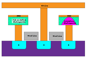
The crystalline and amorphous states of chalcogenide glass have dramatically different electrical resistivity
. The amorphous, high resistance state represents a binary
0, while the crystalline, low resistance state represents a 1. Chalcogenide is the same material used in re-writable optical media (such as CD-RW
and DVD-RW
). In those instances, the material's optical properties are manipulated, rather than its electrical resistivity, as chalcogenide's refractive index
also changes with the state of the material.
Although PRAM has not yet reached the commercialization stage for consumer electronic devices, nearly all prototype devices make use of a chalcogenide
alloy of germanium
, antimony
and tellurium (GeSbTe
) called GST. The stoichiometry
or Ge:Sb:Te element ratio is 2:2:5. When GST is heated to a high temperature (over 600°C), its chalcogenide crystallinity is lost. Once cooled, it is frozen into an amorphous glass-like state and its electrical resistance
is high. By heating the chalcogenide to a temperature above its crystallization point
, but below the melting point
, it will transform into a crystalline state with a much lower resistance. The time to complete this phase transition is temperature-dependent. Cooler portions of the chalcogenide take longer to crystallize, and overheated portions may be remelted. A crystallization time scale on the order of 100 ns is commonly used. This is longer than conventional volatile memory devices like modern DRAM
, which have a switching time on the order of two nanoseconds. However, a January 2006 Samsung Electronics patent application indicates PRAM may achieve switching times as fast as five nanoseconds.
A more recent advance pioneered by Intel and ST Microelectronics allows the material state to be more carefully controlled, allowing it to be transformed into one of four distinct states; the previous amorphic or crystalline states, along with two new partially crystalline ones. Each of these states has different electrical properties that can be measured during reads, allowing a single cell to represent two bits, doubling memory density.
Flash memory works by modulating charge (electron
s) stored within the gate of a MOS transistor
. The gate is constructed with a special "stack" designed to trap charges (either on a floating gate or in insulator "traps"
). The presence of charge within the gate shifts the transistor's threshold voltage
, higher or lower, corresponding to a 1 to 0, for instance. Changing the bit's state requires removing the accumulated charge, which demands a relatively large voltage to "suck" the electrons off the floating gate. This burst of voltage is provided by a charge pump
, which takes some time to build up power. General write times for common Flash devices are on the order of 0.1ms (for a block of data), about 10,000 times the typical 10 ns read time, for SRAM for example (for a byte).
PRAM can offer much higher performance in applications where writing quickly is important, both because the memory element can be switched more quickly, and also because single bits may be changed to either 1 or 0 without needing to first erase an entire block of cells. PRAM's high performance, thousands of times quicker than conventional hard drives, makes it particularly interesting in nonvolatile memory roles that are currently performance-limited by memory access timing.
In addition, with Flash, each burst of voltage across the cell causes degradation. As the size of the cells decreases, damage from programming grows worse because the voltage necessary to program the device does not scale with the lithography. Most flash devices are rated for, currently, only 5,000 writes per sector, and many flash controllers perform wear leveling
to spread writes across many physical sectors.
PRAM devices also degrade with use, for different reasons than Flash, but degrade much more slowly. A PRAM device may endure around 100 million write cycles. PRAM lifetime is limited by mechanisms such as degradation due to GST thermal expansion during programming, metal (and other material) migration, and other mechanisms still unknown.
Flash parts can be programmed before being soldered on to a board
, or even purchased pre-programmed. The contents of a PRAM, however, are lost because of the high temperatures needed to solder the device to a board (see reflow soldering
or wave soldering
). This is made worse by the recent drive to lead-free
manufacturing requiring higher soldering temperatures. The manufacturer using PRAM parts must provide a mechanism to program the PRAM "in-system" after it has been soldered in place.
The special gates used in Flash memory "leak" charge (electrons) over time, causing corruption and loss of data. The resistivity of the memory element in PCM is more stable; at the normal working temperature of 85°C, it is projected to retain data for 300 years.
By carefully modulating the amount of charge stored on the gate, Flash devices can store multiple (usually two) bits in each physical cell. In effect, this doubles the memory density, reducing cost. PRAM devices originally stored only a single bit in each cell, but Intel's recent advances have removed this problem.
Because Flash devices trap electrons to store information, they are susceptible to data corruption from radiation, making them unsuitable for many space and military applications. PRAM exhibits higher resistance to radiation.
PRAM cell selectors can use various devices: diode
s, BJTs
and MOSFET
s. Using a diode or a BJT provides the greatest amount of current for a given cell size. However, the concern with using a diode stems from parasitic currents to neighboring cells, as well as a higher voltage requirement, resulting in higher power consumption. The chalcogenide resistance being a necessarily larger resistance than the diode entails that the operating voltage must exceed 1 V by a wide margin to guarantee adequate forward bias current from the diode. Perhaps the most severe consequence of using a diode-selected array, in particular for large arrays, is the total reverse bias leakage current from the unselected bit lines. In transistor-selected arrays, only the selected bit lines contribute reverse bias leakage current. The difference in leakage current is several orders of magnitude. A further concern with scaling below 40 nm is the effect of discrete dopants as the p-n junction width scales down.
(micro-electric-mechanical-systems) probe storage devices. These devices are not solid state. Instead, a very small platter coated in chalcogenide is dragged beneath many (thousands or even millions) of electrical probes that can read and write the chalcogenide. Hewlett-Packard's micro-mover technology can accurately position the platter to 3 nm so densities of more than 1 Tbit (125 GB) per square inch will be possible if the technology can be perfected. The basic idea is to reduce the amount of wiring needed on-chip; instead of wiring every cell, the cells are placed closer together and read by current passing through the MEMS probes, acting like wires. This approach bears much resemblance to IBM's Millipede
technology.
In September 2006, Samsung
announced a prototype 512 Mb (64 MB) device using diode switches. The announcement was something of a surprise, and it was especially notable for its fairly high density. The prototype featured a cell size of only 46.7 nm, smaller than commercial Flash devices available at the time. Although Flash devices of higher capacity were available (64 Gb, or 8 GB, was just coming to market), other technologies competing to replace Flash in general offered lower densities (larger cell sizes). The only production MRAM
and FeRAM devices are only 4 Mb, for example. The high density of Samsung's prototype PRAM device suggested it could be a viable Flash competitor, and not limited to niche roles as other devices have been. PRAM appeared to be particularly attractive as a potential replacement for NOR Flash, where device capacities typically lag behind those of NAND
Flash devices. (State-of-the-art capacities on NAND passed 512 Mb some time ago.) NOR Flash offers similar densities to Samsung's PRAM prototype and already offers bit addressability (unlike NAND where memory is accessed in banks of many bytes at a time).
Samsung's announcement was followed by one from Intel and STMicroelectronics
, who demonstrated their own PCM devices at the 2006 Intel Developer Forum
in October. They showed a 128 Mb part that recently began manufacture at STMicroelectronics's research lab in Agrate, Italy. Intel stated that the devices were strictly proof-of-concept, but they expect to start sampling within months, and have widespread commercial production within a few years. Intel appears to be aiming their PCM products at the same market as Samsung.
PCM is also a promising technology in the military and aerospace industries where radiation effects make the use of standard non-volatile memories such as Flash impractical. PCM memory devices have been introduced by BAE Systems
, referred to as C-RAM, claiming excellent radiation tolerance (rad-hard) and latchup
immunity. In addition, BAE claims a write cycle endurance of 108, which will allow it to be a contender for replacing PROM
s and EEPROM
s in space systems.
In February 2008, Intel engineers, in cooperation with STMicroelectronics, revealed the first multilevel (MLC
) PCM array prototype. The prototype stored two logical bits in each physical cell, in effect 256 Mb of memory stored in a 128 Mb physical array. This means that instead of the normal two states—fully amorphous and fully crystalline—an additional two distinct intermediate states represent different degrees of partial crystallization, allowing for twice as many bits to be stored in the same physical area on the chip.
Also in February 2008, Intel and STMicroelectronics began shipping prototype samples of their first PCM product released to customers. The 90 nm, 128 Mb (16 MB) product is called Alverstone.
In June 2009, Samsung and Numonyx B.V. announced a collaborative effort in the development of PCM market tailored hardware products that would revolutionise the memory industry in terms of design and efficient in production.
In April 2010, Numonyx announced the Omneo line of 128-Mbit NOR-compatible phase-change memories and Samsung announced shipment of it 512 Mb phase-change RAM (PRAM) in a multi-chip package (MCP) for use in mobile handsets by Fall 2010.
In June 2011, IBM announced that they had created stable, reliable, multi-bit phase change memory with high performance and stability.
The contact between the hot phase-change region and the adjacent dielectric is another fundamental concern. The dielectric may begin to leak current at higher temperature, or may lose adhesion when expanding at a different rate from the phase-change material.
Phase-change memory is susceptible to a fundamental tradeoff of unintended vs. intended phase-change. This stems primarily from the fact that phase-change is a thermally driven process rather than an electronic process. Thermal conditions that allow for fast crystallization should not be too similar to standby conditions, e.g. room temperature. Otherwise data retention cannot be sustained. With the proper activation energy for crystallization it is possible to have fast crystallization at programming conditions while having very slow crystallization at normal conditions.
Probably the biggest challenge for phase change memory is its long-term resistance and threshold voltage drift. The resistance of the amorphous state slowly increases according to a power law (~t0.1). This severely limits the ability for multilevel operation (a lower intermediate state would be confused with a higher intermediate state at a later time) and could also jeopardize standard two-state operation if the threshold voltage increases beyond the design value.
In April 2010, Numonyx released its Omneo line of parallel and serial interface 128 Mb NOR-Flash replacement PCM chips. Although the NOR flash chips they intended to replace operated in the -40-85 °C range, the PCM chips operated in the 0-70°C range, indicating a smaller operating window compared to NOR flash. This is likely due to the use of highly temperature sensitive p-n junctions to provide the high currents needed for programming.
NVRAM
Non-volatile random-access memory is random-access memory that retains its information when power is turned off, which is described technically as being non-volatile...
. PRAMs exploit the unique behavior of chalcogenide glass
Chalcogenide glass
A chalcogenide glass is a glass containing one or more chalcogenide elements. These are Group 16 in the periodic table e.g. sulfur, selenium or tellurium. Such glasses are covalently bonded materials and may be classified as network solids. In effect, the entire glass matrix acts like an...
. Heat produced by the passage of an electric current switches this material between two states, crystal
Crystal
A crystal or crystalline solid is a solid material whose constituent atoms, molecules, or ions are arranged in an orderly repeating pattern extending in all three spatial dimensions. The scientific study of crystals and crystal formation is known as crystallography...
line and amorphous
Amorphous solid
In condensed matter physics, an amorphous or non-crystalline solid is a solid that lacks the long-range order characteristic of a crystal....
. Recent versions can achieve two additional distinct states, in effect doubling their storage capacity. PRAM is one of several new memory technologies competing in the non-volatile role with the almost universal flash memory
Flash memory
Flash memory is a non-volatile computer storage chip that can be electrically erased and reprogrammed. It was developed from EEPROM and must be erased in fairly large blocks before these can be rewritten with new data...
. The latter technology has a number of practical problems that these replacements hope to address.
Background
In the 1960s, Stanford R. Ovshinsky of Energy Conversion Devices first explored the properties of chalcogenide glasses as a potential memory technology. In 1969, Charles Sie published a dissertation, at Iowa State University that both described and demonstrated the feasibility of a phase change memory device by integrating chalcogenide film with a diodeDiode
In electronics, a diode is a type of two-terminal electronic component with a nonlinear current–voltage characteristic. A semiconductor diode, the most common type today, is a crystalline piece of semiconductor material connected to two electrical terminals...
array. A cinematographic study in 1970 established that the phase change memory mechanism in chalcogenide glass involves electric-field-induced crystalline filament growth. In the September 1970 issue of Electronics
Electronics (magazine)
Electronics was an American trade journal that covered the radio industry and its later spin-offs in the mid to late 1900s. Published by McGraw-Hill and Penton Publishing , its first issue was dated in April 1930....
, Gordon Moore
Gordon Moore
Gordon Earle Moore is the co-founder and Chairman Emeritus of Intel Corporation and the author of Moore's Law .-Life and career:...
— co-founder of Intel — published an article on the technology. However, material quality and power consumption issues prevented commercialization of the technology. More recently, interest and research have resumed as flash and DRAM
Dynamic random access memory
Dynamic random-access memory is a type of random-access memory that stores each bit of data in a separate capacitor within an integrated circuit. The capacitor can be either charged or discharged; these two states are taken to represent the two values of a bit, conventionally called 0 and 1...
memory technologies are expected to encounter scaling difficulties as chip lithography
Lithography
Lithography is a method for printing using a stone or a metal plate with a completely smooth surface...
shrinks.
The crystalline and amorphous states of chalcogenide glass have dramatically different electrical resistivity
Resistivity
Electrical resistivity is a measure of how strongly a material opposes the flow of electric current. A low resistivity indicates a material that readily allows the movement of electric charge. The SI unit of electrical resistivity is the ohm metre...
. The amorphous, high resistance state represents a binary
Binary numeral system
The binary numeral system, or base-2 number system, represents numeric values using two symbols, 0 and 1. More specifically, the usual base-2 system is a positional notation with a radix of 2...
0, while the crystalline, low resistance state represents a 1. Chalcogenide is the same material used in re-writable optical media (such as CD-RW
CD-RW
A CD-RW is a rewritable optical disc. It was introduced in 1997, and was known as "CD-Writable" during development. It was preceded by the CD-MO, which was never commercially released....
and DVD-RW
DVD-RW
A DVD-RW disc is a rewritable optical disc with equal storage capacity to a DVD-R, typically 4.7 GB. The format was developed by Pioneer in November 1999 and has been approved by the DVD Forum. The smaller Mini DVD-RW holds 1.46 GB, with a diameter of 8 cm.The primary advantage of DVD-RW over...
). In those instances, the material's optical properties are manipulated, rather than its electrical resistivity, as chalcogenide's refractive index
Refractive index
In optics the refractive index or index of refraction of a substance or medium is a measure of the speed of light in that medium. It is expressed as a ratio of the speed of light in vacuum relative to that in the considered medium....
also changes with the state of the material.
Although PRAM has not yet reached the commercialization stage for consumer electronic devices, nearly all prototype devices make use of a chalcogenide
Chalcogenide
A chalcogenide is a chemical compound consisting of at least one chalcogen ion and at least one more electropositive element. Although all group 16 elements of the periodic table are defined as chalcogens, the term is more commonly reserved for sulfides, selenides, and tellurides, rather than...
alloy of germanium
Germanium
Germanium is a chemical element with the symbol Ge and atomic number 32. It is a lustrous, hard, grayish-white metalloid in the carbon group, chemically similar to its group neighbors tin and silicon. The isolated element is a semiconductor, with an appearance most similar to elemental silicon....
, antimony
Antimony
Antimony is a toxic chemical element with the symbol Sb and an atomic number of 51. A lustrous grey metalloid, it is found in nature mainly as the sulfide mineral stibnite...
and tellurium (GeSbTe
GeSbTe
GeSbTe, Germanium-Antimony-Tellurium or GST is a phase change material from the group of chalcogenide glasses, used in rewritable optical discs and phase-change memory applications. Its recrystallization time is 20 nanoseconds, allowing bitrates of up to 35 Mbit/s to be written, and direct...
) called GST. The stoichiometry
Stoichiometry
Stoichiometry is a branch of chemistry that deals with the relative quantities of reactants and products in chemical reactions. In a balanced chemical reaction, the relations among quantities of reactants and products typically form a ratio of whole numbers...
or Ge:Sb:Te element ratio is 2:2:5. When GST is heated to a high temperature (over 600°C), its chalcogenide crystallinity is lost. Once cooled, it is frozen into an amorphous glass-like state and its electrical resistance
Electrical resistance
The electrical resistance of an electrical element is the opposition to the passage of an electric current through that element; the inverse quantity is electrical conductance, the ease at which an electric current passes. Electrical resistance shares some conceptual parallels with the mechanical...
is high. By heating the chalcogenide to a temperature above its crystallization point
Crystallization
Crystallization is the process of formation of solid crystals precipitating from a solution, melt or more rarely deposited directly from a gas. Crystallization is also a chemical solid–liquid separation technique, in which mass transfer of a solute from the liquid solution to a pure solid...
, but below the melting point
Melting point
The melting point of a solid is the temperature at which it changes state from solid to liquid. At the melting point the solid and liquid phase exist in equilibrium. The melting point of a substance depends on pressure and is usually specified at standard atmospheric pressure...
, it will transform into a crystalline state with a much lower resistance. The time to complete this phase transition is temperature-dependent. Cooler portions of the chalcogenide take longer to crystallize, and overheated portions may be remelted. A crystallization time scale on the order of 100 ns is commonly used. This is longer than conventional volatile memory devices like modern DRAM
Dram
Dram or DRAM may refer to:As a unit of measure:* Dram , an imperial unit of mass and volume* Armenian dram, a monetary unit* Dirham, a unit of currency in several Arab nationsOther uses:...
, which have a switching time on the order of two nanoseconds. However, a January 2006 Samsung Electronics patent application indicates PRAM may achieve switching times as fast as five nanoseconds.
A more recent advance pioneered by Intel and ST Microelectronics allows the material state to be more carefully controlled, allowing it to be transformed into one of four distinct states; the previous amorphic or crystalline states, along with two new partially crystalline ones. Each of these states has different electrical properties that can be measured during reads, allowing a single cell to represent two bits, doubling memory density.
PRAM vs. Flash
It is the switching time and inherent scalability that makes PRAM most appealing. PRAM's temperature sensitivity is perhaps its most notable drawback, one that may require changes in the production process of manufacturers incorporating the technology.Flash memory works by modulating charge (electron
Electron
The electron is a subatomic particle with a negative elementary electric charge. It has no known components or substructure; in other words, it is generally thought to be an elementary particle. An electron has a mass that is approximately 1/1836 that of the proton...
s) stored within the gate of a MOS transistor
MOSFET
The metal–oxide–semiconductor field-effect transistor is a transistor used for amplifying or switching electronic signals. The basic principle of this kind of transistor was first patented by Julius Edgar Lilienfeld in 1925...
. The gate is constructed with a special "stack" designed to trap charges (either on a floating gate or in insulator "traps"
Charge trap flash
Charge Trap Flash is a new technology for the fabrication of NAND flash devices. It was invented by Samsung Electronics in 2006. The technology depends on a SONOS or MONOS capacitor structure, storing the information in charge traps in the nitride layer.-Further reading:* Kinam Kim, "Technology...
). The presence of charge within the gate shifts the transistor's threshold voltage
Threshold voltage
The threshold voltage of a MOSFET is usually defined as the gate voltage where an inversion layer forms at the interface between the insulating layer and the substrate of the transistor. The purpose of the inversion layer's forming is to allow the flow of electrons through the gate-source junction...
,
higher or lower, corresponding to a 1 to 0, for instance. Changing the bit's state requires removing the accumulated charge, which demands a relatively large voltage to "suck" the electrons off the floating gate. This burst of voltage is provided by a charge pumpCharge pump
A charge pump is a kind of DC to DC converter that uses capacitors as energy storage elements to create either a higher or lower voltage power source. Charge pump circuits are capable of high efficiencies, sometimes as high as 90–95% while being electrically simple circuits.Charge pumps use some...
, which takes some time to build up power. General write times for common Flash devices are on the order of 0.1ms (for a block of data), about 10,000 times the typical 10 ns read time, for SRAM for example (for a byte).
PRAM can offer much higher performance in applications where writing quickly is important, both because the memory element can be switched more quickly, and also because single bits may be changed to either 1 or 0 without needing to first erase an entire block of cells. PRAM's high performance, thousands of times quicker than conventional hard drives, makes it particularly interesting in nonvolatile memory roles that are currently performance-limited by memory access timing.
In addition, with Flash, each burst of voltage across the cell causes degradation. As the size of the cells decreases, damage from programming grows worse because the voltage necessary to program the device does not scale with the lithography. Most flash devices are rated for, currently, only 5,000 writes per sector, and many flash controllers perform wear leveling
Wear leveling
Wear leveling is a technique for prolonging the service life of some kinds of erasable computer storage media, such as Flash memory used in solid-state drives and USB Flash drives...
to spread writes across many physical sectors.
PRAM devices also degrade with use, for different reasons than Flash, but degrade much more slowly. A PRAM device may endure around 100 million write cycles. PRAM lifetime is limited by mechanisms such as degradation due to GST thermal expansion during programming, metal (and other material) migration, and other mechanisms still unknown.
Flash parts can be programmed before being soldered on to a board
Printed circuit board
A printed circuit board, or PCB, is used to mechanically support and electrically connect electronic components using conductive pathways, tracks or signal traces etched from copper sheets laminated onto a non-conductive substrate. It is also referred to as printed wiring board or etched wiring...
, or even purchased pre-programmed. The contents of a PRAM, however, are lost because of the high temperatures needed to solder the device to a board (see reflow soldering
Reflow soldering
Reflow soldering is a process in which a solder paste is used to temporarily attach one or several electrical components to their contact pads, after which the entire assembly is subjected to controlled heat, which melts the solder, permanently connecting the joint...
or wave soldering
Wave soldering
Wave soldering is a large-scale soldering process by which electronic components are soldered to a printed circuit board to form an electronic assembly. The name is derived from the use of waves of molten solder to attach metal components to the PCB...
). This is made worse by the recent drive to lead-free
Restriction of Hazardous Substances Directive
The Directive on the restriction of the use of certain hazardous substances in electrical and electronic equipment 2002/95/EC was adopted in February 2003 by the European Union. The RoHS directive took effect on 1 July 2006, and is required to be enforced and become law in each member state...
manufacturing requiring higher soldering temperatures. The manufacturer using PRAM parts must provide a mechanism to program the PRAM "in-system" after it has been soldered in place.
The special gates used in Flash memory "leak" charge (electrons) over time, causing corruption and loss of data. The resistivity of the memory element in PCM is more stable; at the normal working temperature of 85°C, it is projected to retain data for 300 years.
By carefully modulating the amount of charge stored on the gate, Flash devices can store multiple (usually two) bits in each physical cell. In effect, this doubles the memory density, reducing cost. PRAM devices originally stored only a single bit in each cell, but Intel's recent advances have removed this problem.
Because Flash devices trap electrons to store information, they are susceptible to data corruption from radiation, making them unsuitable for many space and military applications. PRAM exhibits higher resistance to radiation.
PRAM cell selectors can use various devices: diode
Diode
In electronics, a diode is a type of two-terminal electronic component with a nonlinear current–voltage characteristic. A semiconductor diode, the most common type today, is a crystalline piece of semiconductor material connected to two electrical terminals...
s, BJTs
Bipolar junction transistor
|- align = "center"| || PNP|- align = "center"| || NPNA bipolar transistor is a three-terminal electronic device constructed of doped semiconductor material and may be used in amplifying or switching applications. Bipolar transistors are so named because their operation involves both electrons...
and MOSFET
MOSFET
The metal–oxide–semiconductor field-effect transistor is a transistor used for amplifying or switching electronic signals. The basic principle of this kind of transistor was first patented by Julius Edgar Lilienfeld in 1925...
s. Using a diode or a BJT provides the greatest amount of current for a given cell size. However, the concern with using a diode stems from parasitic currents to neighboring cells, as well as a higher voltage requirement, resulting in higher power consumption. The chalcogenide resistance being a necessarily larger resistance than the diode entails that the operating voltage must exceed 1 V by a wide margin to guarantee adequate forward bias current from the diode. Perhaps the most severe consequence of using a diode-selected array, in particular for large arrays, is the total reverse bias leakage current from the unselected bit lines. In transistor-selected arrays, only the selected bit lines contribute reverse bias leakage current. The difference in leakage current is several orders of magnitude. A further concern with scaling below 40 nm is the effect of discrete dopants as the p-n junction width scales down.
2000 and later
In August 2004, Nanochip licensed PRAM technology for use in MEMSMicroelectromechanical systems
Microelectromechanical systems is the technology of very small mechanical devices driven by electricity; it merges at the nano-scale into nanoelectromechanical systems and nanotechnology...
(micro-electric-mechanical-systems) probe storage devices. These devices are not solid state. Instead, a very small platter coated in chalcogenide is dragged beneath many (thousands or even millions) of electrical probes that can read and write the chalcogenide. Hewlett-Packard's micro-mover technology can accurately position the platter to 3 nm so densities of more than 1 Tbit (125 GB) per square inch will be possible if the technology can be perfected. The basic idea is to reduce the amount of wiring needed on-chip; instead of wiring every cell, the cells are placed closer together and read by current passing through the MEMS probes, acting like wires. This approach bears much resemblance to IBM's Millipede
IBM Millipede
Millipede is a non-volatile computer memory stored on nanoscopic pits burned into the surface of a thin polymer layer, read and written by a MEMS-based probe...
technology.
In September 2006, Samsung
Samsung
The Samsung Group is a South Korean multinational conglomerate corporation headquartered in Samsung Town, Seoul, South Korea...
announced a prototype 512 Mb (64 MB) device using diode switches. The announcement was something of a surprise, and it was especially notable for its fairly high density. The prototype featured a cell size of only 46.7 nm, smaller than commercial Flash devices available at the time. Although Flash devices of higher capacity were available (64 Gb, or 8 GB, was just coming to market), other technologies competing to replace Flash in general offered lower densities (larger cell sizes). The only production MRAM
MRAM
Magnetoresistive Random-Access Memory is a non-volatile computer memory technology that has been under development since the 1990s. Continued increases in density of existing memory technologies – notably flash RAM and DRAM – kept it in a niche role in the market, but its proponents...
and FeRAM devices are only 4 Mb, for example. The high density of Samsung's prototype PRAM device suggested it could be a viable Flash competitor, and not limited to niche roles as other devices have been. PRAM appeared to be particularly attractive as a potential replacement for NOR Flash, where device capacities typically lag behind those of NAND
Nand
NAND may stand for:*Nand , an Indian classical raga.*Logical NAND , a binary operation in logic.**NAND gate, an electronic gate that implements a logical NAND....
Flash devices. (State-of-the-art capacities on NAND passed 512 Mb some time ago.) NOR Flash offers similar densities to Samsung's PRAM prototype and already offers bit addressability (unlike NAND where memory is accessed in banks of many bytes at a time).
Samsung's announcement was followed by one from Intel and STMicroelectronics
STMicroelectronics
STMicroelectronics is an Italian-French electronics and semiconductor manufacturer headquartered in Geneva, Switzerland.While STMicroelectronics corporate headquarters and the headquarters for EMEA region are based in Geneva, the holding company, STMicroelectronics N.V. is registered in Amsterdam,...
, who demonstrated their own PCM devices at the 2006 Intel Developer Forum
Intel Developer Forum
Intel Developer Forum , is a gathering of technologists to discuss Intel products and products based around Intel products. The first IDF was in 1997...
in October. They showed a 128 Mb part that recently began manufacture at STMicroelectronics's research lab in Agrate, Italy. Intel stated that the devices were strictly proof-of-concept, but they expect to start sampling within months, and have widespread commercial production within a few years. Intel appears to be aiming their PCM products at the same market as Samsung.
PCM is also a promising technology in the military and aerospace industries where radiation effects make the use of standard non-volatile memories such as Flash impractical. PCM memory devices have been introduced by BAE Systems
BAE Systems
BAE Systems plc is a British multinational defence, security and aerospace company headquartered in London, United Kingdom, that has global interests, particularly in North America through its subsidiary BAE Systems Inc. BAE is among the world's largest military contractors; in 2009 it was the...
, referred to as C-RAM, claiming excellent radiation tolerance (rad-hard) and latchup
Latchup
Latchup is a term used in the realm of integrated circuits to describe a particular type of short circuit which can occur in an improperly designed circuit...
immunity. In addition, BAE claims a write cycle endurance of 108, which will allow it to be a contender for replacing PROM
Programmable read-only memory
A programmable read-only memory or field programmable read-only memory or one-time programmable non-volatile memory is a form of digital memory where the setting of each bit is locked by a fuse or antifuse. Such PROMs are used to store programs permanently...
s and EEPROM
EEPROM
EEPROM stands for Electrically Erasable Programmable Read-Only Memory and is a type of non-volatile memory used in computers and other electronic devices to store small amounts of data that must be saved when power is removed, e.g., calibration...
s in space systems.
In February 2008, Intel engineers, in cooperation with STMicroelectronics, revealed the first multilevel (MLC
Multi-level cell
In electronics, a multi-level cell is a memory element capable of storing more than a single bit of information.MLC NAND flash is a flash memory technology using multiple levels per cell to allow more bits to be stored using the same number of transistors...
) PCM array prototype. The prototype stored two logical bits in each physical cell, in effect 256 Mb of memory stored in a 128 Mb physical array. This means that instead of the normal two states—fully amorphous and fully crystalline—an additional two distinct intermediate states represent different degrees of partial crystallization, allowing for twice as many bits to be stored in the same physical area on the chip.
Also in February 2008, Intel and STMicroelectronics began shipping prototype samples of their first PCM product released to customers. The 90 nm, 128 Mb (16 MB) product is called Alverstone.
In June 2009, Samsung and Numonyx B.V. announced a collaborative effort in the development of PCM market tailored hardware products that would revolutionise the memory industry in terms of design and efficient in production.
In April 2010, Numonyx announced the Omneo line of 128-Mbit NOR-compatible phase-change memories and Samsung announced shipment of it 512 Mb phase-change RAM (PRAM) in a multi-chip package (MCP) for use in mobile handsets by Fall 2010.
In June 2011, IBM announced that they had created stable, reliable, multi-bit phase change memory with high performance and stability.
Challenges
The greatest challenge for phase-change memory has been the requirement of high programming current density (>107 A/cm², compared to 105-106 A/cm² for a typical transistor or diode) in the active volume. This has led to active areas that are much smaller than the driving transistor area. The discrepancy has forced phase-change memory structures to package the heater and sometimes the phase-change material itself in sublithographic dimensions. This is a process cost disadvantage compared to Flash.The contact between the hot phase-change region and the adjacent dielectric is another fundamental concern. The dielectric may begin to leak current at higher temperature, or may lose adhesion when expanding at a different rate from the phase-change material.
Phase-change memory is susceptible to a fundamental tradeoff of unintended vs. intended phase-change. This stems primarily from the fact that phase-change is a thermally driven process rather than an electronic process. Thermal conditions that allow for fast crystallization should not be too similar to standby conditions, e.g. room temperature. Otherwise data retention cannot be sustained. With the proper activation energy for crystallization it is possible to have fast crystallization at programming conditions while having very slow crystallization at normal conditions.
Probably the biggest challenge for phase change memory is its long-term resistance and threshold voltage drift. The resistance of the amorphous state slowly increases according to a power law (~t0.1). This severely limits the ability for multilevel operation (a lower intermediate state would be confused with a higher intermediate state at a later time) and could also jeopardize standard two-state operation if the threshold voltage increases beyond the design value.
In April 2010, Numonyx released its Omneo line of parallel and serial interface 128 Mb NOR-Flash replacement PCM chips. Although the NOR flash chips they intended to replace operated in the -40-85 °C range, the PCM chips operated in the 0-70°C range, indicating a smaller operating window compared to NOR flash. This is likely due to the use of highly temperature sensitive p-n junctions to provide the high currents needed for programming.
Timeline
- January 1955: Kolomiets and Gorunova revealed semiconducting properties of chalcogenide glassChalcogenide glassA chalcogenide glass is a glass containing one or more chalcogenide elements. These are Group 16 in the periodic table e.g. sulfur, selenium or tellurium. Such glasses are covalently bonded materials and may be classified as network solids. In effect, the entire glass matrix acts like an...
es. - September 1966: Stanford Ovshinsky files first patent on phase change technology
- January 1969: Charles H. Sie published a dissertation at Iowa State University on chalcogenide phase change memory device
- June 1969: US Patent 3,448,302 (D. J. Shanefield) licensed to Ovshinsky claims first reliable operation of PCM device
- September 1970: Gordon MooreGordon MooreGordon Earle Moore is the co-founder and Chairman Emeritus of Intel Corporation and the author of Moore's Law .-Life and career:...
publishes research in Electronics Magazine - June 1999: Ovonyx joint venture is formed to commercialize PRAM technology
- November 1999: Lockheed Martin works with Ovonyx on PRAM for space applications
- February 2000: Intel invests in Ovonyx, licenses technology
- December 2000: ST Microelectronics licenses PRAM technology from Ovonyx
- March 2002: Macronix files a patent application for transistor-less PRAM
- July 2003: Samsung begins work on PRAM technology
- 2003 through 2005: PRAM-related patent applications filed by Toshiba, Hitachi, Macronix, Renesas, Elpida, Sony, Matsushita, Mitsubishi, Infineon and more
- August 2004: Nanochip licenses PRAM technology from Ovonyx for use in MEMS probe storage
- August 2004: Samsung announces successful 64 Mbit PRAM array
- February 2005: Elpida licenses PRAM technology from Ovonyx
- September 2005: Samsung announces successful 256 Mbit PRAM array, touts 400 µA programming current
- October 2005: Intel increases investment in Ovonyx
- December 2005; Hitachi and Renesas announce 1.5 V PRAM with 100 µA programming current
- December 2005: Samsung licenses PRAM technology from Ovonyx
- July 2006: BAE Systems begins selling the first commercial PRAM, a Radiation Hardened C-RAM 512Kx8 chip
- September 2006: Samsung announces 512 Mbit PRAM device
- October 2006: Intel and STMicroelectronics show a 128 Mbit PRAM chip
- December 2006: IBM Research Labs demonstrate a prototype 3 by 20 nanometers
- January 2007: QimondaQimondaQimonda AG, was a memory company split out of Infineon Technologies on 1 May 2006, to form at the time the second largest DRAM company worldwide, according to the industry research firm Gartner Dataquest...
licenses PRAM technology from Ovonyx - April 2007: Intel's chief technology officer Justin Rattner is set to give the first public demonstration of the company's PRAM (phase-change RAM) technology
- October 2007: HynixHynixHynix Semiconductor Inc. chips and flash memory chips. Founded in 1983, Hynix is the world's second-largest memory chipmaker, the largest being Samsung Electronics. Formerly known as Hyundai Electronics, the company has manufacturing sites in Korea, the U.S., China and Taiwan...
begins pursuing PRAM by licensing Ovonyx' technology - February 2008: Intel and STMicroelectronics announce four-state MLC PRAM and begin shipping samples to customers.
- December 2008: Numonyx announces mass production 128 Mbit PCM device to selected customer.
- June 2009: Samsung's phase change RAM will go into mass production starting in June
- September 2009: Samsung announces mass production start of 512 Mbit PRAM device
- October 2009: Intel and Numonyx announce they have found a way to stack phase change memory arrays on one die
- December 2009: Numonyx announces 1 Gb 45 nm product
- April 2010: Numonyx releases Omneo PCM Series (P8P and P5Q), both in 90 nm.
- April 2010: Samsung releases 512Mbit PCM with 65 nm process, in Multi-Chip-Package.