

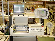
Wave soldering
Encyclopedia
Soldering
Soldering is a process in which two or more metal items are joined together by melting and flowing a filler metal into the joint, the filler metal having a lower melting point than the workpiece...
process by which electronic component
Electronic component
An electronic component is a basic electronic element and may be available in a discrete form having two or more electrical terminals . These are intended to be connected together, usually by soldering to a printed circuit board, in order to create an electronic circuit with a particular function...
s are soldered to a printed circuit board
Printed circuit board
A printed circuit board, or PCB, is used to mechanically support and electrically connect electronic components using conductive pathways, tracks or signal traces etched from copper sheets laminated onto a non-conductive substrate. It is also referred to as printed wiring board or etched wiring...
(PCB) to form an electronic assembly. The name is derived from the use of waves of molten solder to attach metal components to the PCB. The process uses a tank to hold a quantity of molten solder; the components are inserted into or placed on the PCB and the loaded PCB is passed across a pumped wave or waterfall of solder. The solder wets the exposed metallic areas of the board (those not protected with solder mask
Solder mask
Solder mask or solder resist is a lacquer-like layer of polymer that provides a permanent protective coating for the copper traces of a printed circuit board and prevents solder from bridging between conductors, thereby preventing short circuits. Solder mask was created primarily to facilitate...
, a protective coating that prevents the solder from bridging between connections), creating a reliable mechanical and electrical connection. The process is much faster and can create a higher quality product than manual soldering of components.
Wave soldering is used for both through-hole
Through-hole technology
Through-hole technology, also spelled "thru-hole", refers to the mounting scheme used for electronic components that involves the use of leads on the components that are inserted into holes drilled in printed circuit boards and soldered to pads on the opposite side either by manual assembly by...
printed circuit assemblies, and surface mount
Surface-mount technology
Surface mount technology is a method for constructing electronic circuits in which the components are mounted directly onto the surface of printed circuit boards . An electronic device so made is called a surface mount device...
. In the latter case, the components are glued by the placement equipment
SMT Placement Equipment
SMT component placement systems, commonly called pick-and-place machines or P&Ps, are robotic machines which are used to place surface-mount devices onto a printed circuit board...
onto the printed circuit board surface before being run through the molten solder wave.
As through-hole components have been largely replaced by surface mount components, wave soldering has been supplanted by reflow soldering
Reflow soldering
Reflow soldering is a process in which a solder paste is used to temporarily attach one or several electrical components to their contact pads, after which the entire assembly is subjected to controlled heat, which melts the solder, permanently connecting the joint...
methods in many large-scale electronics applications. However, there is still significant wave soldering where SMT is not suitable (e.g. large power devices and high pin count connectors), or where simple through-hole technology prevails (certain major appliance
Major appliance
A major appliance, or domestic appliance, is usually defined as a large machine which accomplishes some routine housekeeping task, which includes purposes such as cooking, or food preservation, whether in a household, institutional, commercial or industrial setting...
s).
Wave solder process
Flux (metallurgy)
In metallurgy, a flux , is a chemical cleaning agent, flowing agent, or purifying agent. Fluxes may have more than one function at a time...
applied. The basic equipment used during the process is a conveyor that moves the PCB through the different zones, a pan of solder used in the soldering process, a pump that produces the actual wave, the sprayer for the flux and the preheating pad. The solder is usually a mixture of metals. A typical solder has the chemical makeup of 50% tin, 49.5% lead, and 0.5% antimony. There are three types of waves: normal wave, a medium speed, long leads used for horizontal soldering; cascade wave, high speed, short leads, used for inclined soldering; and flat wave with extenders; medium to high speeds, long leads that is used for horizontal soldering.
Process Characteristics
The following are characteristics of the wave soldering process:- The solder connection is very reliable and also a clean connection
- The process is automated
- The process reuses the flux and solder that is left over
- It does require inspection, some touch ups, and also testing
- The productivity and efficiency is increased
Fluxing
The PCB first enters the fluxing zone, a fluxer applies flux to the underside of the board. Three types of fluxers are used: spray fluxers, foam fluxers, and rotary fluxers (least common).Spray fluxer
Some spray fluxers consist of a robotic arm which travels from side to side while spraying a fine mistMist
Mist is a phenomenon of small droplets suspended in air. It can occur as part of natural weather or volcanic activity, and is common in cold air above warmer water, in exhaled air in the cold, and in a steam room of a sauna. It can also be created artificially with aerosol canisters if the...
of flux onto the bottom side of the board. Other spray fluxers consist of a stationary bar with a series of nozzles that spray a fine mist. There are also additional ones that can consist of a single stationary ultrasonic head and/or an oscillating ultrasonic head. Some systems will then use compressed air
Compressed air
Compressed air is air which is kept under a certain pressure, usually greater than that of the atmosphere. In Europe, 10 percent of all electricity used by industry is used to produce compressed air, amounting to 80 terawatt hours consumption per year....
to remove excess flux or to completely remove flux from some areas.
Foam fluxer
The foam fluxer consists of a tank of flux into which a plastic cylinder with tiny holes is immersed; this is sometimes called a "stone". The plastic cylinder is covered with a metal chimneyChimney
A chimney is a structure for venting hot flue gases or smoke from a boiler, stove, furnace or fireplace to the outside atmosphere. Chimneys are typically vertical, or as near as possible to vertical, to ensure that the gases flow smoothly, drawing air into the combustion in what is known as the...
. Air is passed through this cylinder which causes flux foam
Foam
-Definition:A foam is a substance that is formed by trapping gas in a liquid or solid in a divided form, i.e. by forming gas regions inside liquid regions, leading to different kinds of dispersed media...
to rise up the chimney, forming a cascading head of foam. As the PCB passes over the foam head, flux is applied to the PCB.
For either flux application method, precise control of flux quantities are required. Too little flux will cause poor joints, while too much flux may cause cosmetic, cleanliness, or other problems. An air knife, can be used ensure flux is evenly applied to the bottom of the circuit board and remove excess flux. Also the types of flux affect the end result. There are two types of flux, corrosive and noncorrosive. Noncorrosive flux requires precleaning and is used when low acidity is required. Corrosive flux is quick and requires little precleaning, but has a higher acidity.
Preheating
Once fluxed, the PCB enters the preheating zone. The preheating zone consists of convection heaters which blow hot air onto the PCB to increase its temperature. For thicker or densely populated PCBs, an upper preheater might be used. The upper preheater is usually an infraredInfrared
Infrared light is electromagnetic radiation with a wavelength longer than that of visible light, measured from the nominal edge of visible red light at 0.74 micrometres , and extending conventionally to 300 µm...
heater.
Preheating is necessary to activate the flux, and to remove any flux carrier solvents. Preheating is also necessary to prevent thermal shock
Thermal shock
Thermal shock is the name given to cracking as a result of rapid temperature change. Glass and ceramic objects are particularly vulnerable to this form of failure, due to their low toughness, low thermal conductivity, and high thermal expansion coefficients...
. Thermal shock occurs when a PCB is suddenly exposed to the high temperature of the molten solder wave.
Soldering
The tank of molten solder has a pattern of standing waveStanding wave
In physics, a standing wave – also known as a stationary wave – is a wave that remains in a constant position.This phenomenon can occur because the medium is moving in the opposite direction to the wave, or it can arise in a stationary medium as a result of interference between two waves traveling...
s (or, in some cases, intermittent waves) on its surface. When the PCB is moved over this tank, the solder waves contact the bottom of the board, and stick to the solder pads and component leads via surface tension
Surface tension
Surface tension is a property of the surface of a liquid that allows it to resist an external force. It is revealed, for example, in floating of some objects on the surface of water, even though they are denser than water, and in the ability of some insects to run on the water surface...
. Precise control of wave height is required to ensure solder is applied to all areas but does not splash to the top of the board or other undesired areas. This process is sometimes performed in an inert
Inert gas
An inert gas is a non-reactive gas used during chemical synthesis, chemical analysis, or preservation of reactive materials. Inert gases are selected for specific settings for which they are functionally inert since the cost of the gas and the cost of purifying the gas are usually a consideration...
nitrogen (N2) atmosphere to increase the quality of the joints. The presence of N2 also reduces oxidization known as solder dross
Dross
Dross is a mass of solid impurities floating on a molten metal. It appears usually on the melting of low-melting-point metals or alloys such as tin, lead, zinc or aluminium, or by oxidation of the metal. It can also consist of impurities such as paint leftovers...
.
Solder dross, its reduction and elimination, is a growing industry concern as lead
Lead
Lead is a main-group element in the carbon group with the symbol Pb and atomic number 82. Lead is a soft, malleable poor metal. It is also counted as one of the heavy metals. Metallic lead has a bluish-white color after being freshly cut, but it soon tarnishes to a dull grayish color when exposed...
soldering is being replaced by lead-free alternatives at significantly higher cost. Dross eliminators are entering the market and may hold some solutions for this concern.
Cleaning
Some types of flux, called "no-clean" fluxes, do not require cleaning; their residues are benign after the soldering process. Others, however, require a cleaning stage, in which the PCB is washed with solventSolvent
A solvent is a liquid, solid, or gas that dissolves another solid, liquid, or gaseous solute, resulting in a solution that is soluble in a certain volume of solvent at a specified temperature...
s and/or deionized water to remove flux residue.
Finish and Quality
Quality depends on proper temperatures when heating and on properly treated surfaces.| Defect | Possible causes | Effects |
|---|---|---|
| Cracks | Mechanical Stress | Loss of Conductivity |
| Cavities | Contaminated surface Lack of flux Insufficient preheating |
Reduction in strength Poor conductivity |
| Wrong solder thickness | Wrong solder temperature Wrong conveyor speed |
Susceptible to stress Too thin for current load Undesired bridging between paths |
| Poor Conductor | Contaminated solder | Product Failures |
Geometrical Possibilities
The typical range of the wire diameter used in wave soldering is about 0.01 in, but the feasible range is from 0.001 in to 0.1 in. The PC board is usually anywhere from about 2 in to 10 in. But it also has a much larger feasible range of about 0.5 in to 600 in.Process monitoring
Due to the precise requirements needed for wave soldering, the soldering equipment must be closely monitored. Common tests include visually inspecting boards for signs of problems such as: bridging- if the wave is too high or too low then the board will not make proper contact with the wave and it can lead to undesirable bridging, causing short circuits. Ventilation does not affect the boards' quality, but if the ventilation in the machine is poor, the fumes from the flux as it goes through the pre-heat can lead to a fire, in which case a foam or powder extinguisher should be used. Due to the extreme temperatures of the wave when it comes into contact with the water, the water flashes off so rapidly it can cause splashes or solder jumping into the air with heights up to 1 meter or even more. Smearing- another flux related problem, is caused by not enough flux being applied during the fluxing stage. Solder sticks to the board and causes streaking. Quality assurance often includes a resistanceElectrical resistance
The electrical resistance of an electrical element is the opposition to the passage of an electric current through that element; the inverse quantity is electrical conductance, the ease at which an electric current passes. Electrical resistance shares some conceptual parallels with the mechanical...
test, to make sure no flux or other deposits cause conduction between traces, halide
Halide
A halide is a binary compound, of which one part is a halogen atom and the other part is an element or radical that is less electronegative than the halogen, to make a fluoride, chloride, bromide, iodide, or astatide compound. Many salts are halides...
content tests to check for proper flux activation, and others. In modern equipment, virtually all control of the process is computerized, with little human interaction needed to monitor and adjust the equipment.
Some defects may occur during the soldering process. Cracks occur due to mechanical stress and can cause loss of conductivity. Cavities, also known as porosity, is caused from either contaminated surfaces, lack of flux, or insufficient heating. Decrease in strength and conductivity is the result. If the wrong solder thickness is produced, the product may be susceptible to stress, or too thin for the load placed upon it. This can be caused by the wrong temperature being used or wrong conveyor speed.
Fixtures
The printed circuit board with through-hole components on top of the board and/or surface mount components glued on the bottom side are sometimes placed on a fixture. The fixture is a fiberglass composite or titanium frame with openings exposing the components to be soldered. Wave solder fixtures are required for PCBs where bottom side components cannot be exposed to the solder, or the board is either too small or has a non rectangular shape and cannot be 'picked up' by the titanium fingers. The fixtures can also be used to incorporate clamping and alignment devices designed to hold components in place and prevent 'lifting' of the components as the leads hit the wave, whilst ensuring correct vertical alignment. In some cases fixtures are also used to reduce changeover time by having fixtures of the same width for different assemblies. This way no changes are needed for the conveyor of the wave solder.The fixture is then placed on a conveyor which will carry the PCB through the machine. The conveyor consists of titanium fingers. Titanium
Titanium
Titanium is a chemical element with the symbol Ti and atomic number 22. It has a low density and is a strong, lustrous, corrosion-resistant transition metal with a silver color....
is used because solder will not adhere to this metal.
The introduction of RoHS
Restriction of Hazardous Substances Directive
The Directive on the restriction of the use of certain hazardous substances in electrical and electronic equipment 2002/95/EC was adopted in February 2003 by the European Union. The RoHS directive took effect on 1 July 2006, and is required to be enforced and become law in each member state...
and the subsequent development of lead free solder (which has a much higher melting point than conventional solder), has caused problems for the manufacturers of material used in fixtures. The higher temperatures causes resin burn out which, in turn, compromises the structural integrity of the fixture. This has created a significant challenge to some manufacturers of both the material and fixtures. Recently fixtures manufactures have introduced higher temperature resistant materials to deal with these challenges. A move from FR4 fiberglass to composite materials has already been made.
Solder types
Although there are many different types of solder that can be used in wave soldering, tin/lead-based solders are the most common. However, these types of solder are quickly being replaced by lead-free solder. Tin/lead-based solder is highly toxic, and government regulations regarding all lead products are becoming increasingly strict. Workers dealing with tin/lead-based solder can be contaminated at work or carry it home on their clothes, where it can cause contamination. Lead-free solder provides a solution to this problem, but it also has its own set of problems that must be taken into consideration.Lead adheres best to copper. The next best metals to use are nickel, brass, aluminum, tungsten, and lastly steel.
Lead-free solder problems
In addition to higher material costs, lead-free solder has a higher melting point, slower flow rates, and can sometimes cause leeching in the iron components. Higher melting points and decreased flow rates require a longer contact period (4 – 6 seconds)between the solder and the connections in order for the solder to completely fill the holes. Higher melting points also require a melting pot made of more stable material. The melting pot and ducts also need to be made from material that will prevent dissolution. Replacing those parts in a typical wave soldering machine can cost up to $25,000.Common solder compositions
Different combinations of tin, lead and other metals are used to create solder. The combinations used depend on the desired properties. The most popular combination is 63% tin, 37% lead. This combination is strong, has a low melting range, and melts and sets quickly. Higher tin compositions gives the solder higher corrosion resistances, but raises the melting point. Another common composition is 11% tin, 37% lead, 42% bismuth, and 10% cadmium. This combination has a low melting point and is useful for soldering components that are sensitive to heat. (Todd p. 395)Defects
Cracks in the solder can occur and are usually caused by stress on the solder and can cause a loss of conductivity. Cavities, pores in the solder, can be caused by contaminated surfaces, insufficient flux, and insufficient preheating. Cavities can reduce strength and conductivity. Improper solder temperature or conveyor speed can cause an undesired thickness. If the solder is too thin, then it is susceptible to stress and may not support the required load. If it is too thick, then unwanted shorts and bridging can occur. Poor conduction in the solder can be caused by contaminated solder and can cause the product to be disfunctional.Excess heat
Excess heat can cause the circuit board to delaminate, become brittle, and become warped. Excess heat can also damage components that are sensitive to heat..Effects of cooling rate
It is important that the PCBs be allowed to cool at a reasonable rate. If they are cooled too fast, then the PCB can become warped and the solder can be compromised. On the other hand if the PCB is allowed to cool too slowly, then the PCB can become brittle and some components may be damaged by heat. The PCB should be cooled by either a fine water spray or air cooled to decrease the amount of damage to the board.Thermal profiling
.svg.png)
Process Window Index
Process Window Index is a statistical measure that quantifies the robustness of a manufacturing process which involves heating and cooling, known as a thermal process...
(PWI) is used to quantify the robustness of a thermal process. PWI helps measure how well a process "fits" into a user-defined process limit known as the Specification Limit.
Each thermal profile is ranked on how it "fits" in a process window (the specification or tolerance limit). The center of the process window is defined as zero, and the extreme edge of the process window as 99%. A PWI greater than or equal to 100% indicates that the profile does not process the product within specification. A PWI of 99% indicates that the profile processes the product within specification, but runs at the edge of the process window. A PWI of 60% indicates a profile uses 60% of the process specification. By using PWI values, manufacturers can determine how much of the process window a particular thermal profile uses. A lower PWI value indicates a more robust profile.
For maximum efficiency, separate PWI values are computed for peak, slope, reflow, and soak processes of a thermal profile. To avoid the possibility of thermal shock affecting the output, the steepest slope in the thermal profile must be determined and leveled. Manufacturers use custom-built software to accurately determine and decrease the steepness of the slope. In addition, the software also automatically recalibrates the PWI values for the peak, slope, reflow, and soak processes. By setting PWI values, engineers can ensure that the reflow soldering work does not overheat or cool too quickly.
Further reading
- Seeling, Karl (1995). A study of lead-free alloys. AIM, 1, Retrieved April 18, 2008, from http://www.aimsolder.com/techarticles/A%20Study%20of%20Lead-Free%20Solder%20Alloys.pdf
- Biocca, Peter (2005, April 5). Lead-free wave soldering. Retrieved April 18, 2008, from EMSnow Web site: http://www.emsnow.com/npps/story.cfm?ID=10669