

Self-assembled monolayer
Encyclopedia
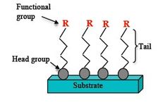
A self assembled monolayer (SAM) is an organized layer of amphiphilic molecules in which one end of the molecule, the “head group” shows a specific, reversible affinity for a substrate. SAMs also consist of a tail with a functional group at the terminal end as seen in Figure 1.
 SAMs are created by the chemisorption
of hydrophilic “head groups” onto a substrate from either the vapor or liquid phase followed by a slow two-dimensional organization of hydrophobic “tail groups”. Initially, adsorbate molecules form either a disordered mass of molecules or form a “lying down phase”, and over a period of minutes to hours, begin to form crystalline or semicrystalline structures on the substrate surface. The hydrophilic “head groups” assemble together on the substrate, while the hydrophobic tail groups assemble far from the substrate. Areas of close-packed molecules nucleate and grow until the surface of the substrate is covered in a single monolayer.
Adsorbate molecules adsorb readily because they lower the surface free-energy of the substrate and are stable due to the strong chemisorption of the “head groups.” These bonds create monolayers that are more stable than the physisorbed bonds of Langmuir–Blodgett films. Thiol-metal bonds, for example, are on the order of 100 kJ/mol, making the bond stable in a wide variety of temperature, solvents, and potentials. The monolayer packs tightly due to van der Waals interactions, thereby reducing its own free energy. The adsorption can be described by the Langmuir adsorption isotherm if lateral interactions are neglected. If they cannot be neglected, the adsorption is better described by the Frumkin isotherm.
and interfacial properties. An appropriate substrate is chosen to react with the head group. Substrates can be planar surfaces, such as silicon and metals, or curved surfaces, such as nanoparticles. Alkanethiols are the most commonly used molecules for SAMs. Alkanethiols are molecules with an alkyl chain, (C-C)ⁿ chain, as the back bone, a tail group, and a S-H head group. They are used on noble metal substrates because of the strong affinity of sulfur for these metals. The sulfur gold interaction is semi-covalent and has a strength of approximately 45kcal/mol. In addition, gold is an inert and biocompatible material that is easy to acquire. It is also easy to pattern via lithography, a useful feature for applications in nanoelectromechanical systems
(NEMS). Additionally, it can withstand harsh chemical cleaning treatments. Silanes are generally used on nonmetallic oxide surfaces; however monolayers formed from covalent bonds between silicon and carbon or oxygen cannot be considered self assembled
because they do not form reversibly
. Self-assembled monolayers of thiolates on noble metals are a special case because the metal-metal bonds become reversible after the formation of the thiolate-metal complex. This reversibility is what gives rise to vacancy islands and it is why SAMs of alkanethiolates can be thermally desorbed and undergo exchange with free thiols.
techniques, electrodeposition
or electroless deposition. Alkanethiol SAMs produced by adsorption from solution are typically made by immersing a substrate into a dilute solution of alkane thiol in ethanol, though many different solvents can be used. While SAMs are often allowed to form over 12 to 72 hours at room temperature, SAMs of alkanethiolates form within minutes. Self-assembled monolayers can also be adsorbed from the vapor phase.
or X-ray photoelectron spectroscopy (XPS)
. Contact angle
measurements can be used to determine the surface free-energy which reflects the average composition of the surface of the SAM and can be used to probe the kinetics and thermodynamics of the formation of SAMs. The structures of SAMs are most commonly determined using scanning probe microscopy techniques such as atomic force microscopy (AFM) and scanning tunneling microscopy (STM). STM has been able to help understand the mechanisms of SAM formation as well as determine the important structural features that lend SAMs their integrity as surface-stable entities. In particular STM can image the shape, spatial distribution, terminal groups and their packing structure. AFM offers an equally powerful tool without the requirement of the SAM being conducting or semi-conducting. AFM has been used to determine chemical functionality, conductance, magnetic properties, surface charge, and frictional forces of SAMs. More recently, however, diffractive methods have also been used. The structure can be used to characterize the kinetics and defects found on the monolayer surface. These techniques have also shown physical differences between SAMs with planar substrates and nanoparticle substrates.
An alternative characterisation instrument for measuring the self assembly in real time is dual polarisation interferometry
where the refractive index, thickness, mass and birefringence of the self assembled layer are quantified at high resolution.

Where θ is the proportional amount of area deposited and k is the rate constant. Although this model is robust it is only used for approximations because it fails to take into account intermediate processes. Dual polarisation interferometry
being a real time technique with ~10Hz resolution can measure the kinetics of monolayer self assembly directly.
Once the molecules are at the surface the self organization occurs in three phases:
The phase transitions in which a SAM forms depends on the temperature of the environment relative to the triple point temperature, the temperature in which the tip of the low density phase intersects with the intermediate phase region. At temperatures below the triple point the growth goes from phase 1 to phase 2 where many islands form with the final SAM structure, but are surrounded by random molecules. Similar to nucleation in metals, as these islands grow larger they intersect forming boundaries until they end up in phase 3, as seen below.
At temperatures above the triple point the growth is more complex and can take two paths. In the first path the heads of the SAM organize to their near final locations with the tail groups loosely formed on top. Then as they transit to phase 3, the tail groups become ordered and straighten out. In the second path the molecules start in a laying down position along the surface. These then form into islands of ordered SAMs, where they grow into phase 3, as seen below.
The nature in which the tail groups organize themselves into a straight ordered monolayer is dependent on the inter-molecular attraction, or Van der Waals forces, between the alkyl and tail groups. To minimize the free energy of the organic layer the molecules adopt conformations that allow high degree of Van der Waals forces with some hydrogen bonding. The small size of the SAM molecules are important here because Van der Waals forces arise from the dipoles of molecules and are thus much weaker than the surrounding surface forces at larger scales. The assembly process begins with a small group of molecules, usually two, getting close enough that the Van der Waals forces overcome the surrounding force. The forces between the molecules orientate themselves so they are in their straight, optimal, configuration. Then as other molecules come close by they interact with these already organized molecules in the same fashion and become a part of the conformed group. When this occurs across a large area the molecules support each other into forming their SAM shape seen in Figure 1. The orientation of the molecules can be described with 2 parameters, α and β. α is the angle of tilt of the backbone from the surface normal. In typical applications α varies from 0 to 60 degrees depending on the substrate and type of SAM molecule. β is the angel of rotation along the long axis of tee molecule. β is usually between 30 and 40 degrees.
Many of the SAM properties, such as thickness, are determined in the first few minutes. However, it may take hours for defects to be eliminated via annealing and for final SAM properties to be determined. The exact kinetics of SAM formation depends on the adsorbate, solvent and substrate properties. In general, however, the kinetics are dependent on both preparations conditions and material properties of the solvent, adsorbate and substrate. Specifically, kinetics for adsorption from a liquid solution are dependent on:
The final structure of the SAM is also dependent on the chain length and the structure of both the adsorbate and the substrate. Steric hindrance and metal substrate properties, for example, can affect the packing density of the film, while chain length affects SAM thickness. Longer chain length also increases the thermodynamic stability.
will later be located. This strategy is advantageous because it involves high throughput methods that generally involve fewer steps than the other two strategies. The major techniques that use this strategy are:
(NEMS) and microelectromechanical systems
(MEMS), and everyday household goods. SAMs can serve as models for studying membrane properties of cells and organelles and cell attachment on surfaces. SAMs can also be used to modify the surface properties of electrodes for electrochemistry, general electronics, and various NEMS and MEMS. For example, the properties of SAMs can be used to control electron transfer in electrochemistry. They can serve to protect metals from harsh chemicals and etchants. SAMs can also reduce sticking of NEMS and MEMS components in humid environments. In the same way, SAMs can alter the properties of glass. A common household product, Rain-X
, utilizes SAMs to create a hydrophobic monolayer on car windshields to keep them clear of rain.
Thin film SAMs can also be placed on nanostructures. In this way they functionalize the nanostructure
. This is advantageous because the nanostructure
can now selectively attach itself to other molecules or SAMs. This technique is useful in biosensors or other MEMS devices that need to separate one type of molecule from its environment. One example is the use of magnetic nanoparticles to remove a fungus
from a blood stream. The nanoparticle
is coated with a SAM that binds to the fungus. As the contaminated blood is filtered through a MEMS device the magnetic nanoparticles are inserted into the blood where they bind to the fungus and are then magnetically driven out of the blood stream into a nearby laminar
waste stream.
s, because each adsorbate molecule can be tailored to attract two different materials. Current techniques utilize the head to attract to a surface, like a plate of gold. The terminal group is then modified to attract a specific material like a particular nanoparticle
, wire, ribbon, or other nanostructure
. In this way, wherever the a SAM is patterned to a surface there will be nanostructures attached to the tail groups. One example is the use of two types of SAMs to align single wall carbon nanotubes, SWNTs. Dip pen nanolithography was used to pattern a 16-mercaptohexadecanoic acid (MHA)SAM and the rest of the surface was passivated with 1-octadecanethiol (ODT) SAM. As the solvent that was carrying the SWNTs evaporated, the SWNTs became attracted to the MHA SAM because of its hydrophilic nature. Once the SWNTs became close enough to the MHA SAM they attached to it due to Van der Waals forces. Using this technique Chad Mirkin
, Schatz and their co-workers were able to make complex two dimensional shapes, a representation of a shape created is shown to the right.
Another application of patterned SAMs is the functionalization of biosensors. The tail groups can be modified so they have an affinity for cells
, proteins, or molecules. The SAM can then be placed onto a biosensor
so that binding of these molecules can be detected. The ability to pattern these SAMs allows them to be placed in configurations that increase sensitivity and do not damage or interfere with other components of the biosensor
.
Chemisorption
Chemisorption is a sub-class of adsorption, driven by a chemical reaction occurring at the exposed surface. A new chemical species is generated at the adsorbant surface...
of hydrophilic “head groups” onto a substrate from either the vapor or liquid phase followed by a slow two-dimensional organization of hydrophobic “tail groups”. Initially, adsorbate molecules form either a disordered mass of molecules or form a “lying down phase”, and over a period of minutes to hours, begin to form crystalline or semicrystalline structures on the substrate surface. The hydrophilic “head groups” assemble together on the substrate, while the hydrophobic tail groups assemble far from the substrate. Areas of close-packed molecules nucleate and grow until the surface of the substrate is covered in a single monolayer.
Adsorbate molecules adsorb readily because they lower the surface free-energy of the substrate and are stable due to the strong chemisorption of the “head groups.” These bonds create monolayers that are more stable than the physisorbed bonds of Langmuir–Blodgett films. Thiol-metal bonds, for example, are on the order of 100 kJ/mol, making the bond stable in a wide variety of temperature, solvents, and potentials. The monolayer packs tightly due to van der Waals interactions, thereby reducing its own free energy. The adsorption can be described by the Langmuir adsorption isotherm if lateral interactions are neglected. If they cannot be neglected, the adsorption is better described by the Frumkin isotherm.
Types of SAMs
Selecting the type of head group depends on the application of the SAM. Typically, head groups are connected to an alkyl chain in which the terminal end can be functionalized (i.e. adding –OH, –NH3, or –COOH groups) to vary the wettingWetting
Wetting is the ability of a liquid to maintain contact with a solid surface, resulting from intermolecular interactions when the two are brought together. The degree of wetting is determined by a force balance between adhesive and cohesive forces.Wetting is important in the bonding or adherence of...
and interfacial properties. An appropriate substrate is chosen to react with the head group. Substrates can be planar surfaces, such as silicon and metals, or curved surfaces, such as nanoparticles. Alkanethiols are the most commonly used molecules for SAMs. Alkanethiols are molecules with an alkyl chain, (C-C)ⁿ chain, as the back bone, a tail group, and a S-H head group. They are used on noble metal substrates because of the strong affinity of sulfur for these metals. The sulfur gold interaction is semi-covalent and has a strength of approximately 45kcal/mol. In addition, gold is an inert and biocompatible material that is easy to acquire. It is also easy to pattern via lithography, a useful feature for applications in nanoelectromechanical systems
Nanoelectromechanical systems
Nanoelectromechanical systems are devices integrating electrical and mechanical functionality on the nanoscale. NEMS form the logical next miniaturization step from so-called microelectromechanical systems, or MEMS devices...
(NEMS). Additionally, it can withstand harsh chemical cleaning treatments. Silanes are generally used on nonmetallic oxide surfaces; however monolayers formed from covalent bonds between silicon and carbon or oxygen cannot be considered self assembled
Self-assembly
Self-assembly is a term used to describe processes in which a disordered system of pre-existing components forms an organized structure or pattern as a consequence of specific, local interactions among the components themselves, without external direction...
because they do not form reversibly
Reversibility
Reversibility can refer to:* Reversible dynamics, a mathematical dynamical system, or physical laws of motion, for which time-reversed dynamics are well defined* Reversible diffusion, an example of a reversible stochastic process...
. Self-assembled monolayers of thiolates on noble metals are a special case because the metal-metal bonds become reversible after the formation of the thiolate-metal complex. This reversibility is what gives rise to vacancy islands and it is why SAMs of alkanethiolates can be thermally desorbed and undergo exchange with free thiols.
Preparation of SAMs
Metal substrates for use in SAMs can be produced through physical vapor depositionPhysical vapor deposition
Physical vapor deposition is a variety of vacuum deposition and is a general term used to describe any of a variety of methods to deposit thin films by the condensation of a vaporized form of the desired film material onto various workpiece surfaces...
techniques, electrodeposition
Electrodeposition
Electrodeposition may refer to:*Electroplating*Electrophoretic deposition*Underpotential deposition...
or electroless deposition. Alkanethiol SAMs produced by adsorption from solution are typically made by immersing a substrate into a dilute solution of alkane thiol in ethanol, though many different solvents can be used. While SAMs are often allowed to form over 12 to 72 hours at room temperature, SAMs of alkanethiolates form within minutes. Self-assembled monolayers can also be adsorbed from the vapor phase.
Characterization of SAMs
The thicknesses of SAMs can be measured using ellipsometryEllipsometry
Ellipsometry is an optical technique for the investigation of the dielectric properties of thin films....
or X-ray photoelectron spectroscopy (XPS)
X-ray photoelectron spectroscopy
X-ray photoelectron spectroscopy is a quantitative spectroscopic technique that measures the elemental composition, empirical formula, chemical state and electronic state of the elements that exist within a material...
. Contact angle
Contact angle
The contact angle is the angle at which a liquid/vapor interface meets a solid surface. The contact angle is specific for any given system and is determined by the interactions across the three interfaces. Most often the concept is illustrated with a small liquid droplet resting on a flat...
measurements can be used to determine the surface free-energy which reflects the average composition of the surface of the SAM and can be used to probe the kinetics and thermodynamics of the formation of SAMs. The structures of SAMs are most commonly determined using scanning probe microscopy techniques such as atomic force microscopy (AFM) and scanning tunneling microscopy (STM). STM has been able to help understand the mechanisms of SAM formation as well as determine the important structural features that lend SAMs their integrity as surface-stable entities. In particular STM can image the shape, spatial distribution, terminal groups and their packing structure. AFM offers an equally powerful tool without the requirement of the SAM being conducting or semi-conducting. AFM has been used to determine chemical functionality, conductance, magnetic properties, surface charge, and frictional forces of SAMs. More recently, however, diffractive methods have also been used. The structure can be used to characterize the kinetics and defects found on the monolayer surface. These techniques have also shown physical differences between SAMs with planar substrates and nanoparticle substrates.
An alternative characterisation instrument for measuring the self assembly in real time is dual polarisation interferometry
Dual Polarisation Interferometry
Dual polarization interferometry is an analytical technique that can probe molecular scale layers adsorbed to the surface of a waveguide by using the evanescent wave of a laser beam confined to the waveguide...
where the refractive index, thickness, mass and birefringence of the self assembled layer are quantified at high resolution.
Defects
Defects due to both external and intrinsic factors may appear. External factors include the cleanliness of the substrate, method of preparation, and purity of the adsorbates. SAMs intrinsically form defects due to the thermodynamics of formation, e.g. thiol SAMs on gold typically exhibit etch pits (monoatomic vacancy islands) likely due to extraction of adatoms from the substrate and formation of adatom-adsorbate moieties.Nanoparticle properties
The structure of SAMs is also dependent on the curvature of the substrate. SAMs on nanoparticles including colloids and nanocrystals, “stabilize the reactive surface of the particle and present organic functional groups at the particle-solvent interface”. These organic functional groups are useful for applications, such as immunoassays, that are dependent on chemical composition of the surface.Kinetics
There is evidence that SAM formation occurs in two steps, an initial fast step of adsorption and a second slower step of monolayer organization. Adsorption occurs at the liquid-liquid, liquid-vapor, and liquid-solid interfaces. The transport of molecules to the surface occurs due to a combination of diffusion and convective transport. According to the Langmuir or Avrami kinetic model the rate of deposition onto the surface is proportional to the free space of the surface.Where θ is the proportional amount of area deposited and k is the rate constant. Although this model is robust it is only used for approximations because it fails to take into account intermediate processes. Dual polarisation interferometry
Dual Polarisation Interferometry
Dual polarization interferometry is an analytical technique that can probe molecular scale layers adsorbed to the surface of a waveguide by using the evanescent wave of a laser beam confined to the waveguide...
being a real time technique with ~10Hz resolution can measure the kinetics of monolayer self assembly directly.
Once the molecules are at the surface the self organization occurs in three phases:
- 1. A low density phase with random dispersion of molecules on the surface.
- 2. An intermediate density phase with conformational disordered molecules or molecules lying flat on the surface.
- 3. A high density phase with close packed order and molecules standing normal to the substrate's surface.
The phase transitions in which a SAM forms depends on the temperature of the environment relative to the triple point temperature, the temperature in which the tip of the low density phase intersects with the intermediate phase region. At temperatures below the triple point the growth goes from phase 1 to phase 2 where many islands form with the final SAM structure, but are surrounded by random molecules. Similar to nucleation in metals, as these islands grow larger they intersect forming boundaries until they end up in phase 3, as seen below.
At temperatures above the triple point the growth is more complex and can take two paths. In the first path the heads of the SAM organize to their near final locations with the tail groups loosely formed on top. Then as they transit to phase 3, the tail groups become ordered and straighten out. In the second path the molecules start in a laying down position along the surface. These then form into islands of ordered SAMs, where they grow into phase 3, as seen below.
The nature in which the tail groups organize themselves into a straight ordered monolayer is dependent on the inter-molecular attraction, or Van der Waals forces, between the alkyl and tail groups. To minimize the free energy of the organic layer the molecules adopt conformations that allow high degree of Van der Waals forces with some hydrogen bonding. The small size of the SAM molecules are important here because Van der Waals forces arise from the dipoles of molecules and are thus much weaker than the surrounding surface forces at larger scales. The assembly process begins with a small group of molecules, usually two, getting close enough that the Van der Waals forces overcome the surrounding force. The forces between the molecules orientate themselves so they are in their straight, optimal, configuration. Then as other molecules come close by they interact with these already organized molecules in the same fashion and become a part of the conformed group. When this occurs across a large area the molecules support each other into forming their SAM shape seen in Figure 1. The orientation of the molecules can be described with 2 parameters, α and β. α is the angle of tilt of the backbone from the surface normal. In typical applications α varies from 0 to 60 degrees depending on the substrate and type of SAM molecule. β is the angel of rotation along the long axis of tee molecule. β is usually between 30 and 40 degrees.
Many of the SAM properties, such as thickness, are determined in the first few minutes. However, it may take hours for defects to be eliminated via annealing and for final SAM properties to be determined. The exact kinetics of SAM formation depends on the adsorbate, solvent and substrate properties. In general, however, the kinetics are dependent on both preparations conditions and material properties of the solvent, adsorbate and substrate. Specifically, kinetics for adsorption from a liquid solution are dependent on:
- Temperature – room temperature preparation improves kinetics and reduces defects.
- Concentration of adsorbate in the solution – low concentrations require longer immersion times and often create highly crystalline domains.
- Purity of the adsorbate – impurities can affect the final physical properties of the SAM
- Dirt or contamination on the substrate – imperfections can cause defects in the SAM
The final structure of the SAM is also dependent on the chain length and the structure of both the adsorbate and the substrate. Steric hindrance and metal substrate properties, for example, can affect the packing density of the film, while chain length affects SAM thickness. Longer chain length also increases the thermodynamic stability.
1. Locally attract
This first strategy involves locally depositing self-assembled monolayers on the surface only where the nanostructureNanostructure
A nanostructure is an object of intermediate size between molecular and microscopic structures.In describing nanostructures it is necessary to differentiate between the number of dimensions on the nanoscale. Nanotextured surfaces have one dimension on the nanoscale, i.e., only the thickness of the...
will later be located. This strategy is advantageous because it involves high throughput methods that generally involve fewer steps than the other two strategies. The major techniques that use this strategy are:
- Micro-contact printingSoft lithography200px|right|thumb|Figure 1 - "Inking" a stamp. PDMS stamp with pattern is placed in Ethanol and ODT solution200px|right|thumb|Figure 2 - ODT from the solution settles down onto the PDMS stamp. Stamp now has ODT attached to it which acts as the ink....
- Micro-contact printing or soft lithographySoft lithography200px|right|thumb|Figure 1 - "Inking" a stamp. PDMS stamp with pattern is placed in Ethanol and ODT solution200px|right|thumb|Figure 2 - ODT from the solution settles down onto the PDMS stamp. Stamp now has ODT attached to it which acts as the ink....
is analogous to printing ink with a rubber stamp. The SAM molecules are inked onto an pre-shaped elastomeric stamp with a solvent and transferred to the substrate surface by stamping. The SAM solution is applied to the entire stamp but only areas that make contact with the surface allow transfer of the SAMs. The transfer of the SAMs is a complex diffusion process that depends on the type of molecule, concentration, duration of contact, and pressure applied. Typical stamps use PDMS because its elastomeric properties, E = 1.8 MPa, allow it to fit the countour of micro surfaces and its low surface energy, γ = 21.6 dyn/cm². This is a parallel process and can thus place nanoscale objects over a large area in a short time.
- Dip-pen nanolithography
- Dip-pen nanolithography is a process that uses an atomic force microscopeAtomic force microscopeAtomic force microscopy or scanning force microscopy is a very high-resolution type of scanning probe microscopy, with demonstrated resolution on the order of fractions of a nanometer, more than 1000 times better than the optical diffraction limit...
to transfer molecules on the tip to a substrate. Initially the tip is dipped into a reservoir with an ink. The ink on the tip evaporates and leaves the desired molecules attached to the tip. When the tip is brought into contact with the surface a water meniscus forms between the tip and the surface resulting in the diffusion of molecules from the tip to the surface. These tips can have radii in the tens of nanometers, and thus SAM molecules can be very precisely deposited onto a specific location of the surface. This process was discovered by Chad MirkinChad MirkinChad A. Mirkin is an American chemist. He is the George B. Rathmann Professor of Chemistry, Professor of Medicine, Professor of Materials Science and Engineering, and Director of the International Institute for Nanotechnology and Center for Nanofabrication and Molecular Self-Assembly at...
and co-workers at Northwestern UniversityNorthwestern UniversityNorthwestern University is a private research university in Evanston and Chicago, Illinois, USA. Northwestern has eleven undergraduate, graduate, and professional schools offering 124 undergraduate degrees and 145 graduate and professional degrees....
.
2. Locally remove
The locally remove strategy begins with covering the entire surface with a SAM. Then individual SAM molecules are removed from locations where the deposition of nanostructures is not desired. The end result is the same as in the locally attract strategy, the difference being in the way this is achieved. The major techniques that use this strategy are:- Scanning tunneling microscopeScanning tunneling microscopeA scanning tunneling microscope is an instrument for imaging surfaces at the atomic level. Its development in 1981 earned its inventors, Gerd Binnig and Heinrich Rohrer , the Nobel Prize in Physics in 1986. For an STM, good resolution is considered to be 0.1 nm lateral resolution and...
- The scanning tunneling microscopeScanning tunneling microscopeA scanning tunneling microscope is an instrument for imaging surfaces at the atomic level. Its development in 1981 earned its inventors, Gerd Binnig and Heinrich Rohrer , the Nobel Prize in Physics in 1986. For an STM, good resolution is considered to be 0.1 nm lateral resolution and...
can remove SAM molecules in many different ways. The first is to remove them mechanically by dragging the tip across the substrate surface. This is not the most desired technique as these tips are expensive and dragging them causes a lot of wear and reduction of the tip quality. The second way is to degrade or desorb the SAM molecules by shooting them with an electron beam. The scanning tunneling microscopeScanning tunneling microscopeA scanning tunneling microscope is an instrument for imaging surfaces at the atomic level. Its development in 1981 earned its inventors, Gerd Binnig and Heinrich Rohrer , the Nobel Prize in Physics in 1986. For an STM, good resolution is considered to be 0.1 nm lateral resolution and...
can also remove SAMs by field desorptionField desorptionField desorption /field ionization refers to an ion source for mass spectrometry first reported by Beckey in 1969. In field ionization, a high-potential electric field is applied to an emitter with a sharp surface, such as a razor blade, or more commonly, a filament from which tiny "whiskers"...
and field enhanced surface diffusion.
- Atomic force microscopeAtomic force microscopeAtomic force microscopy or scanning force microscopy is a very high-resolution type of scanning probe microscopy, with demonstrated resolution on the order of fractions of a nanometer, more than 1000 times better than the optical diffraction limit...
- The most common use of this technique is to remove the SAM molecules in a process called shaving, where the atomic force microscopeAtomic force microscopeAtomic force microscopy or scanning force microscopy is a very high-resolution type of scanning probe microscopy, with demonstrated resolution on the order of fractions of a nanometer, more than 1000 times better than the optical diffraction limit...
tip is dragged along the surface mechanically removing the molecules. An atomic force microscopeAtomic force microscopeAtomic force microscopy or scanning force microscopy is a very high-resolution type of scanning probe microscopy, with demonstrated resolution on the order of fractions of a nanometer, more than 1000 times better than the optical diffraction limit...
can also remove SAM molecules by local oxidation nanolithographyLocal oxidation nanolithographyLocal oxidation nanolithography is a tip-based nanofabrication method. It is based on the spatial confinement on an oxidation reaction under the sharp tip of an atomic force microscope....
.
- UltravioletUltravioletUltraviolet light is electromagnetic radiation with a wavelength shorter than that of visible light, but longer than X-rays, in the range 10 nm to 400 nm, and energies from 3 eV to 124 eV...
irradiation
- In this process, UV light is projected onto the surface with a SAM through a pattern of apperatures in a chromium film. This leads to photo oxidation of the SAM molecules. These can then be washed away in a polar solvent. This process has 100nm resolutions and requires exposure time of 15-20 minutes.
3. Modify tail groups
The final strategy focuses not on the deposition or removal of SAMS, but the modification of terminal groups. In the first case the terminal group can be modified to remove functionality so that SAM molecule will be inert. In the same regards the terminal group can be modified to add functionality so it can accept different materials or have different properties than the original SAM terminal group. The major techniques that use this strategy are:- Focused electron beam and ultravioletUltravioletUltraviolet light is electromagnetic radiation with a wavelength shorter than that of visible light, but longer than X-rays, in the range 10 nm to 400 nm, and energies from 3 eV to 124 eV...
irradiation
- Exposure to electron beams and UV light changes the terminal group chemistry. Some of the changes that can occur include the cleavage of bonds, the forming of double carbon bonds, cross-linking of adjacent molecules, fragmentation of molecules, and confromational disorder.
- Atomic force microscopeAtomic force microscopeAtomic force microscopy or scanning force microscopy is a very high-resolution type of scanning probe microscopy, with demonstrated resolution on the order of fractions of a nanometer, more than 1000 times better than the optical diffraction limit...
- A conductive AFM tip can create an electrochemical reaction that can change the terminal group.
Thin Film SAMs
SAMs are an inexpensive and versatile surface coating for applications including control of wetting and adhesion, chemical resistance, bio compatibility, sensitization, and molecular recognition for sensors and nano fabrication. Areas of application for SAMs include biology, electrochemistry and electronics, nanoelectromechanical systemsNanoelectromechanical systems
Nanoelectromechanical systems are devices integrating electrical and mechanical functionality on the nanoscale. NEMS form the logical next miniaturization step from so-called microelectromechanical systems, or MEMS devices...
(NEMS) and microelectromechanical systems
Microelectromechanical systems
Microelectromechanical systems is the technology of very small mechanical devices driven by electricity; it merges at the nano-scale into nanoelectromechanical systems and nanotechnology...
(MEMS), and everyday household goods. SAMs can serve as models for studying membrane properties of cells and organelles and cell attachment on surfaces. SAMs can also be used to modify the surface properties of electrodes for electrochemistry, general electronics, and various NEMS and MEMS. For example, the properties of SAMs can be used to control electron transfer in electrochemistry. They can serve to protect metals from harsh chemicals and etchants. SAMs can also reduce sticking of NEMS and MEMS components in humid environments. In the same way, SAMs can alter the properties of glass. A common household product, Rain-X
Rain-X
Rain-X is a line of consumer automotive and surface care products produced by SOPUS Products , a subsidiary of Royal Dutch Shell. Industrial Rain-X products are produced by Ecolab and used in carwashes and other industrial applications...
, utilizes SAMs to create a hydrophobic monolayer on car windshields to keep them clear of rain.
Thin film SAMs can also be placed on nanostructures. In this way they functionalize the nanostructure
Nanostructure
A nanostructure is an object of intermediate size between molecular and microscopic structures.In describing nanostructures it is necessary to differentiate between the number of dimensions on the nanoscale. Nanotextured surfaces have one dimension on the nanoscale, i.e., only the thickness of the...
. This is advantageous because the nanostructure
Nanostructure
A nanostructure is an object of intermediate size between molecular and microscopic structures.In describing nanostructures it is necessary to differentiate between the number of dimensions on the nanoscale. Nanotextured surfaces have one dimension on the nanoscale, i.e., only the thickness of the...
can now selectively attach itself to other molecules or SAMs. This technique is useful in biosensors or other MEMS devices that need to separate one type of molecule from its environment. One example is the use of magnetic nanoparticles to remove a fungus
Fungus
A fungus is a member of a large group of eukaryotic organisms that includes microorganisms such as yeasts and molds , as well as the more familiar mushrooms. These organisms are classified as a kingdom, Fungi, which is separate from plants, animals, and bacteria...
from a blood stream. The nanoparticle
Nanoparticle
In nanotechnology, a particle is defined as a small object that behaves as a whole unit in terms of its transport and properties. Particles are further classified according to size : in terms of diameter, coarse particles cover a range between 10,000 and 2,500 nanometers. Fine particles are sized...
is coated with a SAM that binds to the fungus. As the contaminated blood is filtered through a MEMS device the magnetic nanoparticles are inserted into the blood where they bind to the fungus and are then magnetically driven out of the blood stream into a nearby laminar
Laminar flow
Laminar flow, sometimes known as streamline flow, occurs when a fluid flows in parallel layers, with no disruption between the layers. At low velocities the fluid tends to flow without lateral mixing, and adjacent layers slide past one another like playing cards. There are no cross currents...
waste stream.
Patterned SAMs
SAMs are also useful in depositing nanostructureNanostructure
A nanostructure is an object of intermediate size between molecular and microscopic structures.In describing nanostructures it is necessary to differentiate between the number of dimensions on the nanoscale. Nanotextured surfaces have one dimension on the nanoscale, i.e., only the thickness of the...
s, because each adsorbate molecule can be tailored to attract two different materials. Current techniques utilize the head to attract to a surface, like a plate of gold. The terminal group is then modified to attract a specific material like a particular nanoparticle
Nanoparticle
In nanotechnology, a particle is defined as a small object that behaves as a whole unit in terms of its transport and properties. Particles are further classified according to size : in terms of diameter, coarse particles cover a range between 10,000 and 2,500 nanometers. Fine particles are sized...
, wire, ribbon, or other nanostructure
Nanostructure
A nanostructure is an object of intermediate size between molecular and microscopic structures.In describing nanostructures it is necessary to differentiate between the number of dimensions on the nanoscale. Nanotextured surfaces have one dimension on the nanoscale, i.e., only the thickness of the...
. In this way, wherever the a SAM is patterned to a surface there will be nanostructures attached to the tail groups. One example is the use of two types of SAMs to align single wall carbon nanotubes, SWNTs. Dip pen nanolithography was used to pattern a 16-mercaptohexadecanoic acid (MHA)SAM and the rest of the surface was passivated with 1-octadecanethiol (ODT) SAM. As the solvent that was carrying the SWNTs evaporated, the SWNTs became attracted to the MHA SAM because of its hydrophilic nature. Once the SWNTs became close enough to the MHA SAM they attached to it due to Van der Waals forces. Using this technique Chad Mirkin
Chad Mirkin
Chad A. Mirkin is an American chemist. He is the George B. Rathmann Professor of Chemistry, Professor of Medicine, Professor of Materials Science and Engineering, and Director of the International Institute for Nanotechnology and Center for Nanofabrication and Molecular Self-Assembly at...
, Schatz and their co-workers were able to make complex two dimensional shapes, a representation of a shape created is shown to the right.
Another application of patterned SAMs is the functionalization of biosensors. The tail groups can be modified so they have an affinity for cells
Cell (biology)
The cell is the basic structural and functional unit of all known living organisms. It is the smallest unit of life that is classified as a living thing, and is often called the building block of life. The Alberts text discusses how the "cellular building blocks" move to shape developing embryos....
, proteins, or molecules. The SAM can then be placed onto a biosensor
Biosensor
A biosensor is an analytical device for the detection of an analyte that combines a biological component with a physicochemical detector component.It consists of 3 parts:* the sensitive biological element A biosensor is an analytical device for the detection of an analyte that combines a biological...
so that binding of these molecules can be detected. The ability to pattern these SAMs allows them to be placed in configurations that increase sensitivity and do not damage or interfere with other components of the biosensor
Biosensor
A biosensor is an analytical device for the detection of an analyte that combines a biological component with a physicochemical detector component.It consists of 3 parts:* the sensitive biological element A biosensor is an analytical device for the detection of an analyte that combines a biological...
.
Further reading
- I. Rubinstein, E. Sabatani, R. Maoz and J. Sagiv, Organized Monolayers on Gold Electrodes, in Electrochemical Sensors for Biomedical Applications, C.K.N. Li (Ed.), The Electrochemical Society 1986: 175.
- N. Faucheux, R. Schweiss, K. Lützow, C. Werner, T. Groth. Self-assembled monolayers with different terminating groups as model substrates for cell adhesion studies. Biomaterials 2004;25:2721-2730.
- S. R. Wasserman, Y. T. Tao, G. M. Whitesides. Structure and Reactivity of Alkylsiloxane Monolayers Formed by Reaction of Alkyltrichlorosilanes on Silicon Substrates. Langmuir 1989;5:1074-1087
- H.E. Hoster, M. Roos, A. Breitruck, C. Meier, K. Tonigold, T. Waldmann, U. Ziener, K. Landfester, R.J. Behm, Structure Formation in Bis(terpyridine)Derivative Adlayers – Molecule-Substrate vs. Molecule-Molecule Interactions, Langmuir 23 (2007) 11570
- Molecular-Self Assembly Webinar
- Sigma-Aldrich "Material Matters", Molecular Self-Assembly
- Structure and Dynamics of Organic Nanostructures
- Metal organic coordination networks of oligopyridines and Cu on graphite
- Surface Alloys
- Dojindo - Surface Assembled Monolayers