

Pentium II
Encyclopedia
The Pentium II brand refers to Intel's sixth-generation microarchitecture
("P6
") and x86
-compatible microprocessor
s introduced on May 7, 1997. Containing 7.5 million transistor
s, the Pentium II featured an improved version of the first P6-generation core of the Pentium Pro
, which contained 5.5 million transistors. However, its L2 cache subsystem was a downgrade when compared to Pentium Pros. In early 1999, the Pentium II was superseded by the Pentium III
.
In 1998, Intel stratified the Pentium II family by releasing the Pentium II-based Celeron
line of processors for low-end workstations and the Pentium II Xeon line for servers and high-end workstations. The Celeron was characterized by a reduced or omitted (in some cases present but disabled) on-die full-speed L2 cache and a 66 MT/s FSB. The Xeon was characterized by a range of full-speed L2 cache (from 512 KB to 2048 KB), a 100 MT/s FSB, a different physical interface (Slot 2
), and support for symmetric multiprocessing
.
of its predecessor, the Pentium Pro
, but with some significant improvements.
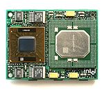
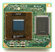
Unlike previous Pentium and Pentium Pro processors, the Pentium II CPU was packaged in a slot
-based module rather than a CPU socket
. The processor and associated components were carried on a daughterboard
similar to a typical expansion board within a plastic cartridge. A fixed or removable heatsink was carried on one side, sometimes using its own fan.
This larger package was a compromise allowing Intel to separate the secondary cache
from the processor while still keeping it on a closely coupled back-side bus. The L2 cache ran at half the processor's clock frequency, unlike the Pentium Pro, whose off die L2 cache ran at the same frequency as the processor. However, the smallest cache size was increased to 512 KB from the 256 KB on the Pentium Pro. Off-package cache solved the Pentium Pro's low yields, allowing Intel to introduce the Pentium II at a mainstream price level. This arrangement also allowed Intel to easily vary the amount of L2 cache, thus making it possible to target different market segments with cheaper or more expensive processors and accompanying performance levels.
Intel notably improved 16-bit
code execution performance on the Pentium II, an area in which the Pentium Pro was at a notable handicap. Most consumer software of the day was still using at least some 16-bit code, because of a variety of factors. The Pentium II went to 32 KB of L1 cache, double that of the Pentium Pro, as well. The Pentium II was also the first P6-based CPU to implement the Intel MMX integer SIMD
instruction set which had already been introduced on the Pentium MMX.
The Pentium II was basically a more consumer-oriented version of the Pentium Pro. It was cheaper to manufacture because of the separate, slower L2 cache memory. The improved 16-bit performance and MMX support made it a better choice for consumer-level operating systems, such as Windows 9x
, and multimedia applications. Combined with the larger L1 cache and improved 16-bit performance, the slower and cheaper L2 cache's performance impact was reduced. General processor performance was increased while costs were cut.
process. A 300 MHz version was released later in 1997. These CPUs had a 66 MHz front side bus
and were initially used on motherboards equipped with the aging Intel 440FX Natoma chipset designed for the Pentium Pro.
In Intel's "Family/Model/Stepping" scheme, Klamath CPUs are family 6, model 3.
process. The 333 MHz variant was the final Pentium CPU that used the older 66 MHz front side bus
; all subsequent Deschutes-core models used a 100 MHz FSB. Later in 1998, Pentium IIs running at 266, 300, 350, 400, and 450 MHz were also released. The Deschutes core supported FXSAVE and FXRSTOR instructions, as opposed to Klamath. The die size was 113 mm 2. Towards the end of its design life, Deschutes chips capable of 500MHz within Intel cooling and design specifications were produced. However, these were not marketed. Rather than destroy already multiplier-locked units, those Deschutes units that had been tested and locked with a multiplier of 5 were sold as being 333MHz. This was accomplished by disabling the 100MHz bus option. Overclockers, upon learning of this, purchased the units in question and ran them well over 500MHz; most notably, when overclocking, the final batch of "333MHz" CPUs were capable of speeds much higher than CPUs sold at 350, 400, or 450 MHz.
Pentium II-based systems using the Intel 440LX Balboa chipset were the first to utilize the new generation RAM-standard, SDRAM
(which replaced EDO RAM
), and the AGP
graphics bus. Concurrent with the release of Deschutes cores supporting a 100 MHz front side bus was Intel's release of the 440BX
Seattle chipset and its related cousins, the 440MX, 440NX, and 440ZX chipsets. Introduction of the 100 MHz front side bus speed resulted in solid performance improvements for the Pentium II lineup.
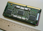
 The Pentium II Xeon was a high-end version of Deschutes core intended for use on workstation
s and server
s. Principally, it used a different type of slot (Slot 2
), case, board design, and more expensive full-speed custom L2 cache, which was off-die. Versions were produced with 512 KB, 1 MB or 2 MB L2 caches by varying the number of 512 KB chips incorporated on the board.
 In Intel's "Family/Model/Stepping" scheme, Deschutes CPUs are family 6, model 5 and have the part number 80523.
users to upgrade their aging servers. Combining the Deschutes core in a flip-chip package with a 512 KB full-speed L2 cache chip from the Pentium II Xeon into a Socket 8
-compatible module resulted in a 300 or 333 MHz processor that could run on a 60 or 66 MHz front side bus. This combination brought together some of the more attractive aspects of the Pentium II and the Pentium II Xeon: MMX support/improved 16-bit performance and full-speed L2 cache, respectively. The later "Dixon" mobile Pentium II would emulate this combination with 256 KB of full-speed cache.
In Intel's "Family/Model/Stepping" scheme, the Pentium II OverDrive CPU identifies itself as family 6, model 3, though this is misleading, as it not based on the family 6/model 3 Klamath core. As noted in the Pentium II Processor update documentation from Intel, "Please note that although this processor has a CPUID of 163xh, it uses a Pentium II processor CPUID 065xh processor core."
In Intel's "Family/Model/Stepping" scheme, Tonga CPUs are family 6, model 5.
In Intel's "Family/Model/Stepping" scheme, Dixon CPUs are family 6, model 6 and their Intel product code is 80524. These identifiers are shared with the Mendocino Celeron processors.
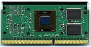
 Mobile Pentium II
 Mobile Pentium II PE ("Performance Enhanced")
Intel datasheets
Microarchitecture
In computer engineering, microarchitecture , also called computer organization, is the way a given instruction set architecture is implemented on a processor. A given ISA may be implemented with different microarchitectures. Implementations might vary due to different goals of a given design or...
("P6
P6 (microarchitecture)
The P6 microarchitecture is the sixth generation Intel x86 microarchitecture, implemented by the Pentium Pro microprocessor that was introduced in November 1995. It is sometimes referred to as i686. It was succeeded by the NetBurst microarchitecture in 2000, but eventually revived in the Pentium M...
") and x86
X86 architecture
The term x86 refers to a family of instruction set architectures based on the Intel 8086 CPU. The 8086 was launched in 1978 as a fully 16-bit extension of Intel's 8-bit based 8080 microprocessor and also introduced segmentation to overcome the 16-bit addressing barrier of such designs...
-compatible microprocessor
Microprocessor
A microprocessor incorporates the functions of a computer's central processing unit on a single integrated circuit, or at most a few integrated circuits. It is a multipurpose, programmable device that accepts digital data as input, processes it according to instructions stored in its memory, and...
s introduced on May 7, 1997. Containing 7.5 million transistor
Transistor
A transistor is a semiconductor device used to amplify and switch electronic signals and power. It is composed of a semiconductor material with at least three terminals for connection to an external circuit. A voltage or current applied to one pair of the transistor's terminals changes the current...
s, the Pentium II featured an improved version of the first P6-generation core of the Pentium Pro
Pentium Pro
The Pentium Pro is a sixth-generation x86 microprocessor developed and manufactured by Intel introduced in November 1, 1995 . It introduced the P6 microarchitecture and was originally intended to replace the original Pentium in a full range of applications...
, which contained 5.5 million transistors. However, its L2 cache subsystem was a downgrade when compared to Pentium Pros. In early 1999, the Pentium II was superseded by the Pentium III
Pentium III
The Pentium III brand refers to Intel's 32-bit x86 desktop and mobile microprocessors based on the sixth-generation P6 microarchitecture introduced on February 26, 1999. The brand's initial processors were very similar to the earlier Pentium II-branded microprocessors...
.
In 1998, Intel stratified the Pentium II family by releasing the Pentium II-based Celeron
Celeron
Celeron is a brand name given by Intel Corp. to a number of different x86 computer microprocessor models targeted at budget personal computers....
line of processors for low-end workstations and the Pentium II Xeon line for servers and high-end workstations. The Celeron was characterized by a reduced or omitted (in some cases present but disabled) on-die full-speed L2 cache and a 66 MT/s FSB. The Xeon was characterized by a range of full-speed L2 cache (from 512 KB to 2048 KB), a 100 MT/s FSB, a different physical interface (Slot 2
Slot 2
Slot 2 refers to the physical and electrical specification for the 330-lead Single Edge Contact Cartridge used by some of Intel's Pentium II Xeon and certain models of the Pentium III Xeon....
), and support for symmetric multiprocessing
Symmetric multiprocessing
In computing, symmetric multiprocessing involves a multiprocessor computer hardware architecture where two or more identical processors are connected to a single shared main memory and are controlled by a single OS instance. Most common multiprocessor systems today use an SMP architecture...
.
Overview
The Pentium II microprocessor was largely based upon the microarchitectureMicroarchitecture
In computer engineering, microarchitecture , also called computer organization, is the way a given instruction set architecture is implemented on a processor. A given ISA may be implemented with different microarchitectures. Implementations might vary due to different goals of a given design or...
of its predecessor, the Pentium Pro
Pentium Pro
The Pentium Pro is a sixth-generation x86 microprocessor developed and manufactured by Intel introduced in November 1, 1995 . It introduced the P6 microarchitecture and was originally intended to replace the original Pentium in a full range of applications...
, but with some significant improvements.
Unlike previous Pentium and Pentium Pro processors, the Pentium II CPU was packaged in a slot
Slot 1
Slot 1 refers to the physical and electrical specification for the connector used by some of Intel's microprocessors, including the Pentium Pro, Celeron, Pentium II and the Pentium III...
-based module rather than a CPU socket
CPU socket
A CPU socket or CPU slot is a mechanical component that provides mechanical and electrical connections between a microprocessor and a printed circuit board . This allows the CPU to be replaced without soldering....
. The processor and associated components were carried on a daughterboard
Daughterboard
A daughterboard, daughtercard or piggyback board is a circuit board meant to be an extension or "daughter" of a motherboard , or occasionally of another card...
similar to a typical expansion board within a plastic cartridge. A fixed or removable heatsink was carried on one side, sometimes using its own fan.
This larger package was a compromise allowing Intel to separate the secondary cache
CPU cache
A CPU cache is a cache used by the central processing unit of a computer to reduce the average time to access memory. The cache is a smaller, faster memory which stores copies of the data from the most frequently used main memory locations...
from the processor while still keeping it on a closely coupled back-side bus. The L2 cache ran at half the processor's clock frequency, unlike the Pentium Pro, whose off die L2 cache ran at the same frequency as the processor. However, the smallest cache size was increased to 512 KB from the 256 KB on the Pentium Pro. Off-package cache solved the Pentium Pro's low yields, allowing Intel to introduce the Pentium II at a mainstream price level. This arrangement also allowed Intel to easily vary the amount of L2 cache, thus making it possible to target different market segments with cheaper or more expensive processors and accompanying performance levels.
Intel notably improved 16-bit
16-bit
-16-bit architecture:The HP BPC, introduced in 1975, was the world's first 16-bit microprocessor. Prominent 16-bit processors include the PDP-11, Intel 8086, Intel 80286 and the WDC 65C816. The Intel 8088 was program-compatible with the Intel 8086, and was 16-bit in that its registers were 16...
code execution performance on the Pentium II, an area in which the Pentium Pro was at a notable handicap. Most consumer software of the day was still using at least some 16-bit code, because of a variety of factors. The Pentium II went to 32 KB of L1 cache, double that of the Pentium Pro, as well. The Pentium II was also the first P6-based CPU to implement the Intel MMX integer SIMD
SIMD
Single instruction, multiple data , is a class of parallel computers in Flynn's taxonomy. It describes computers with multiple processing elements that perform the same operation on multiple data simultaneously...
instruction set which had already been introduced on the Pentium MMX.
The Pentium II was basically a more consumer-oriented version of the Pentium Pro. It was cheaper to manufacture because of the separate, slower L2 cache memory. The improved 16-bit performance and MMX support made it a better choice for consumer-level operating systems, such as Windows 9x
Windows 9x
Windows 9x is a generic term referring to a series of Microsoft Windows computer operating systems produced since 1995, which were based on the original and later modified Windows 95 kernel...
, and multimedia applications. Combined with the larger L1 cache and improved 16-bit performance, the slower and cheaper L2 cache's performance impact was reduced. General processor performance was increased while costs were cut.
Klamath
The original Klamath Pentium II microprocessor (Intel product code 80522) ran at 233 and 266 MHz and were produced in a 0.35 µmMicrometre
A micrometer , is by definition 1×10⁻⁶ of a meter .In plain English, it means one-millionth of a meter . Its unit symbol in the International System of Units is μm...
process. A 300 MHz version was released later in 1997. These CPUs had a 66 MHz front side bus
Front side bus
A front-side bus is a computer communication interface often used in computers during the 1990s and 2000s.It typically carries data between the central processing unit and a memory controller hub, known as the northbridge....
and were initially used on motherboards equipped with the aging Intel 440FX Natoma chipset designed for the Pentium Pro.
In Intel's "Family/Model/Stepping" scheme, Klamath CPUs are family 6, model 3.
Deschutes
The Deschutes core Pentium II (80523), which debuted at 333 MHz in January 1998, was produced with a 0.25 µmMicrometre
A micrometer , is by definition 1×10⁻⁶ of a meter .In plain English, it means one-millionth of a meter . Its unit symbol in the International System of Units is μm...
process. The 333 MHz variant was the final Pentium CPU that used the older 66 MHz front side bus
Front side bus
A front-side bus is a computer communication interface often used in computers during the 1990s and 2000s.It typically carries data between the central processing unit and a memory controller hub, known as the northbridge....
; all subsequent Deschutes-core models used a 100 MHz FSB. Later in 1998, Pentium IIs running at 266, 300, 350, 400, and 450 MHz were also released. The Deschutes core supported FXSAVE and FXRSTOR instructions, as opposed to Klamath. The die size was 113 mm 2. Towards the end of its design life, Deschutes chips capable of 500MHz within Intel cooling and design specifications were produced. However, these were not marketed. Rather than destroy already multiplier-locked units, those Deschutes units that had been tested and locked with a multiplier of 5 were sold as being 333MHz. This was accomplished by disabling the 100MHz bus option. Overclockers, upon learning of this, purchased the units in question and ran them well over 500MHz; most notably, when overclocking, the final batch of "333MHz" CPUs were capable of speeds much higher than CPUs sold at 350, 400, or 450 MHz.
Pentium II-based systems using the Intel 440LX Balboa chipset were the first to utilize the new generation RAM-standard, SDRAM
SDRAM
Synchronous dynamic random access memory is dynamic random access memory that is synchronized with the system bus. Classic DRAM has an asynchronous interface, which means that it responds as quickly as possible to changes in control inputs...
(which replaced EDO RAM
Dynamic random access memory
Dynamic random-access memory is a type of random-access memory that stores each bit of data in a separate capacitor within an integrated circuit. The capacitor can be either charged or discharged; these two states are taken to represent the two values of a bit, conventionally called 0 and 1...
), and the AGP
Accelerated Graphics Port
The Accelerated Graphics Port is a high-speed point-to-point channel for attaching a video card to a computer's motherboard, primarily to assist in the acceleration of 3D computer graphics. Since 2004 AGP has been progressively phased out in favor of PCI Express...
graphics bus. Concurrent with the release of Deschutes cores supporting a 100 MHz front side bus was Intel's release of the 440BX
Intel 440BX
The Intel 440BX , is a chipset from Intel, supporting Pentium II, Pentium III, and Celeron processors. It is also known as the i440BX and was released in April 1998...
Seattle chipset and its related cousins, the 440MX, 440NX, and 440ZX chipsets. Introduction of the 100 MHz front side bus speed resulted in solid performance improvements for the Pentium II lineup.
Workstation
A workstation is a high-end microcomputer designed for technical or scientific applications. Intended primarily to be used by one person at a time, they are commonly connected to a local area network and run multi-user operating systems...
s and server
Server (computing)
In the context of client-server architecture, a server is a computer program running to serve the requests of other programs, the "clients". Thus, the "server" performs some computational task on behalf of "clients"...
s. Principally, it used a different type of slot (Slot 2
Slot 2
Slot 2 refers to the physical and electrical specification for the 330-lead Single Edge Contact Cartridge used by some of Intel's Pentium II Xeon and certain models of the Pentium III Xeon....
), case, board design, and more expensive full-speed custom L2 cache, which was off-die. Versions were produced with 512 KB, 1 MB or 2 MB L2 caches by varying the number of 512 KB chips incorporated on the board.
Pentium II OverDrive
In 1998, the 0.25 μm Deschutes core was utilized in the creation of the Pentium II Overdrive processor, which was aimed at allowing corporate Pentium ProPentium Pro
The Pentium Pro is a sixth-generation x86 microprocessor developed and manufactured by Intel introduced in November 1, 1995 . It introduced the P6 microarchitecture and was originally intended to replace the original Pentium in a full range of applications...
users to upgrade their aging servers. Combining the Deschutes core in a flip-chip package with a 512 KB full-speed L2 cache chip from the Pentium II Xeon into a Socket 8
Socket 8
The Socket 8 CPU socket was used exclusively with the Intel Pentium Pro and Pentium II Overdrive computer processors. Intel discontinued Socket 8 in favor of Slot 1 with the introduction of the Pentium II.-Technical specifications:...
-compatible module resulted in a 300 or 333 MHz processor that could run on a 60 or 66 MHz front side bus. This combination brought together some of the more attractive aspects of the Pentium II and the Pentium II Xeon: MMX support/improved 16-bit performance and full-speed L2 cache, respectively. The later "Dixon" mobile Pentium II would emulate this combination with 256 KB of full-speed cache.
In Intel's "Family/Model/Stepping" scheme, the Pentium II OverDrive CPU identifies itself as family 6, model 3, though this is misleading, as it not based on the family 6/model 3 Klamath core. As noted in the Pentium II Processor update documentation from Intel, "Please note that although this processor has a CPUID of 163xh, it uses a Pentium II processor CPUID 065xh processor core."
Tonga
The 0.25 μm Tonga core was the first mobile Pentium II and had all of the features of the desktop models.In Intel's "Family/Model/Stepping" scheme, Tonga CPUs are family 6, model 5.
Dixon
Later, in 1999, the 0.25 μm Dixon core with 256 KB of on-die full speed cache was produced for the mobile market. Reviews showed that the Dixon core was the fastest type of Pentium II produced.In Intel's "Family/Model/Stepping" scheme, Dixon CPUs are family 6, model 6 and their Intel product code is 80524. These identifiers are shared with the Mendocino Celeron processors.
Desktop
Klamath (80522)
- L1 cache: 16 + 16 KB (Data + Instructions)
- L2 cache: 512 KB, as external chips on the CPU module clocked at half the CPU frequency.
- Packaging: Slot 1Slot 1Slot 1 refers to the physical and electrical specification for the connector used by some of Intel's microprocessors, including the Pentium Pro, Celeron, Pentium II and the Pentium III...
module - MMX
- Front-side bus: 66 MHz, GTL+
- VCore: 2.8 V
- Process: 0.35 µm CMOS
- First release: May 7, 1997
- Clockrate: 233, 266, 300 MHz
Deschutes (80523)
- L1 cache: 16 + 16 KB (Data + Instructions)
- L2 cache: 512 KB, as external chips on the CPU module clocked at half the CPU frequency.
- Packaging: Slot 1Slot 1Slot 1 refers to the physical and electrical specification for the connector used by some of Intel's microprocessors, including the Pentium Pro, Celeron, Pentium II and the Pentium III...
module - MMX
- Front-side bus: 66, 100 MHz, GTL+
- VCore: 2.0 V
- Process: 0.25 µm CMOS
- First release: January 26, 1998
- Clockrate: 266 - 450 MHz
- 66 MHz FSB : 266, 300, 333 MHz
- 100 MHz FSB: 350, 400, 450 MHz
Deschutes (Pentium II Overdrive)
- L1 cache: 16 + 16 KB (Data + Instructions)
- L2 cache: 512 KB external chip on CPU module running at 100% of CPU speed
- Socket: Socket 8Socket 8The Socket 8 CPU socket was used exclusively with the Intel Pentium Pro and Pentium II Overdrive computer processors. Intel discontinued Socket 8 in favor of Slot 1 with the introduction of the Pentium II.-Technical specifications:...
- Front-side bus: 60 or 66 MHz, GTL+
- VCore: 3.1-3.3 V (Has on-board voltage regulator)
- Fabrication: 0.25 µm
- Based on the Deschutes-generation Pentium II
- First release: 1998
- Supports MMX technology
- The sSpec number SL2KE denotes a Pentium II Overdrive sold with an integrated heatsink/fan combination for Socket 8. [Note that the sSpec number SL2EA denotes a Pentium II Overdrive sold with an integrated heatsink but no fan for Slot 1.]
Tonga (80523)
- L1 cache: 16 + 16 KB (Data + Instructions)
- L2 cache: 512 KB, as external chips on the CPU module clocked at half the CPU frequency.
- Package: MMC-1MMC-1Mobile Module Connector 1 , is a 280-pin microprocessor cartridge developed by Intel for used by their mobile Pentium, Pentium MMX, Pentium II and Celeron processors...
, MMC-2MMC-2Mobile Module Connector 2, Intel's 400 pin processor cartridge used with Pentium II, Celeron and Pentium III mobile processors. It contains CPU, 443BX Northbridge, L2 Cache and voltage regulator. It is successor of MMC-1, main differences being AGP interface and 100 MHz FSB for the Pentium...
, Mini-CartridgeMini-CartridgeThe Mini-Cartridge or Mobile Mini-Cartridge was Intel's 240-pin multi-chip module for their mobile Pentium II processors. It contained the CPU core, as well as separate cache chips and a thermal sensor.... - MMX
- Front side busFront side busA front-side bus is a computer communication interface often used in computers during the 1990s and 2000s.It typically carries data between the central processing unit and a memory controller hub, known as the northbridge....
: 66 MHz, GTL+ - VCore: 1.6 V
- Process: 0.25 µm CMOS
- First release: June 7, 1997
- Clockrate: 233, 266, 300 MHz
Dixon (80524)
- L1 cache: 16 + 16 KB (Data + Instructions)
- L2 cache: 256 KB, on-die, full speed.
- Package: BGA1BGA1Intel's ball grid array package for their Pentium II and early Celeron mobile processors. For newer processors, the successor BGA2 was used....
, MMC-1MMC-1Mobile Module Connector 1 , is a 280-pin microprocessor cartridge developed by Intel for used by their mobile Pentium, Pentium MMX, Pentium II and Celeron processors...
, MMC-2MMC-2Mobile Module Connector 2, Intel's 400 pin processor cartridge used with Pentium II, Celeron and Pentium III mobile processors. It contains CPU, 443BX Northbridge, L2 Cache and voltage regulator. It is successor of MMC-1, main differences being AGP interface and 100 MHz FSB for the Pentium...
, μPGA1 - MMX
- Front-side bus: 66, 100 MHz, GTL+
- VCore: 1.5, 1.55, 1.6 V, 2.0 V
- Process: 0.25 µm CMOS
- First release: January 25, 1999
- Clockrate: 266, 300, 333, 366, 400 MHz
External links
- Listing of various PII, PIII, and Celeron alphanumeric model designations
- CPU-INFO: Intel Pentium II, indepth processor history
Intel datasheets