Microbolometer
Encyclopedia
A microbolometer is a specific type of bolometer
used as a detector in a thermal camera. Infrared
radiation
with wavelength
s between 7.5-14 μm strikes the detector material, heating it, and thus changing its electrical resistance
. This resistance change is measured and processed into temperatures which can be used to create an image. Unlike other types of infrared detecting equipment, microbolometers do not require cooling.
. Previous high resolution thermal sensors required exotic and expensive cooling methods including stirling cycle
coolers and liquid nitrogen
coolers. These methods of cooling made early thermal imagers expensive to operate and unwieldy to move. Also, older thermal imagers required a cool down time in excess of 10 minutes before being usable.

A microbolometer consists of an array of pixel
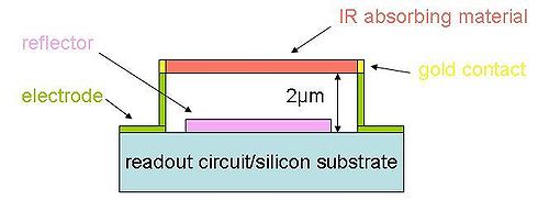
s, each pixel being made up of several layers. The cross-sectional diagram shown in Figure 1 provides a generalized view of the pixel. Each company that manufactures microbolometers has their own unique procedure for producing them and they even use a variety of different absorbing materials. In this example the bottom layer consists of a silicon
substrate and a readout integrated circuit (ROIC). Electrical contacts are deposited and then selectively etched away. A reflector, for example, a titanium mirror, is created beneath the IR absorbing material. Since some light is able to pass through the absorbing layer, the reflector redirects this light back up to ensure the greatest possible absorption, hence allowing a stronger signal to be produced. Next, a sacrificial layer is deposited so that later in the process a gap can be created to thermally isolate the IR absorbing material from the ROIC. A layer of absorbing material is then deposited and selectively etched so that the final contacts can be created. To create the final bridge like structure shown in Figure 1, the sacrificial layer is removed so that the absorbing material is suspended approximately 2 μm above the readout circuit. Because microbolometers do not undergo any cooling, the absorbing material must be thermally isolated from the bottom ROIC and the bridge like structure allows for this to occur. After the array of pixels is created the microbolometer is encapsulated under a vacuum to increase the longevity of the device. In some cases the entire fabrication process is done without breaking vacuum.
The quality of images created from microbolometers has continued to increase. The microbolometer array is commonly found in two sizes, 320×240 pixels or less expensive 160×120 pixels. Current technology has led to the production of devices with 640×480 or 1024x768 pixels. There has also been a decrease in the individual pixel dimensions. The pixel size was typically 45 μm in older devices and has been decreased to 17 μm in current devices. As the pixel size is decreased and the number of pixels per unit area is increased proportionally, an image with higher resolution is created.
. Responsivity is the ability of the device to convert the incoming radiation into an electrical signal. Detector material properties influence this value and thus several main material properties should be investigated: TCR, 1/f Noise, and Resistance.
(TCR) specifically its negative temperature coefficient. Industry currently manufactures microbolometers that contain materials with TCRs near -2%. Although many materials exist that have far higher TCRs, there are several other factors that need to be taken into consideration when producing optimized microbolometers.
, like other noises, causes a disturbance that affects the signal and that may distort the information carried by the signal. Changes in temperature across the absorbing material are determined by changes in the bias current
or voltage
flowing through the detecting material. If the noise is large then small changes that occur may not be seen clearly and the device is useless. Using a detector material that has a minimum amount of 1/f noise allows for a clearer signal to be maintained between IR detection and the output that is displayed. Detector material must be tested to assure that this noise does not significantly interfere with signal.
and vanadium oxide
. Much research has been done to test other materials feasibility to be used as a detecting material. Other materials that have been investigated include: Ti, YBaCuO, GeSiO, poly SiGe
, BiLaSrMnO and a protein based cytochrome C
and bovine serum albumin
.
Amorphous Si (a-Si) works well mainly because it can easily be integrated into the CMOS fabrication process. To create the layered structure and patterning, the CMOS
fabrication process can be used but it requires temperatures to stay below 200˚C on average. A problem with some potential materials is that to create the desirable properties their deposition temperatures may be too high although this is not a problem for a-Si thin films. a-Si also possesses reasonable values for TCR, 1/f noise and resistance when the deposition parameters are optimized.
Vanadium oxide thin films may also be integrated into the CMOS fabrication process although not as easily as a-Si for temperature reasons. Deposition at high temperatures and performing post-annealing
allows for the production of films with superior properties although acceptable films can still be made subsequently fulfilling the temperature requirements. VO2 has low resistance but undergoes a metal-insulator phase change near 67oC and also has a lower value of TCR. On the other hand, V2O5 exhibits high resistance and also high TCR. Many phases of VOx exist although it seems that x≈1.8 has become the most popular for microbolometer applications.
divided by the thermal conductance. Reducing the heat capacity increases the speed but also increases statistical mechanical
thermal temperature fluctuations (noise). Increasing the thermal conductance raises the speed, but decreases sensitivity.
starting in the late 70's as a classified contract for the US Department of Defense. The US Government declassified the technology in 1992. After declassification Honeywell licensed their technology to several manufacturers.

Bolometer
A bolometer is a device for measuring the power of incident electromagnetic radiation via the heating of a material with a temperature-dependent electrical resistance. It was invented in 1878 by the American astronomer Samuel Pierpont Langley...
used as a detector in a thermal camera. Infrared
Infrared
Infrared light is electromagnetic radiation with a wavelength longer than that of visible light, measured from the nominal edge of visible red light at 0.74 micrometres , and extending conventionally to 300 µm...
radiation
Radiation
In physics, radiation is a process in which energetic particles or energetic waves travel through a medium or space. There are two distinct types of radiation; ionizing and non-ionizing...
with wavelength
Wavelength
In physics, the wavelength of a sinusoidal wave is the spatial period of the wave—the distance over which the wave's shape repeats.It is usually determined by considering the distance between consecutive corresponding points of the same phase, such as crests, troughs, or zero crossings, and is a...
s between 7.5-14 μm strikes the detector material, heating it, and thus changing its electrical resistance
Electrical resistance
The electrical resistance of an electrical element is the opposition to the passage of an electric current through that element; the inverse quantity is electrical conductance, the ease at which an electric current passes. Electrical resistance shares some conceptual parallels with the mechanical...
. This resistance change is measured and processed into temperatures which can be used to create an image. Unlike other types of infrared detecting equipment, microbolometers do not require cooling.
Theory of operation
A microbolometer is an uncooled thermal sensorSensor
A sensor is a device that measures a physical quantity and converts it into a signal which can be read by an observer or by an instrument. For example, a mercury-in-glass thermometer converts the measured temperature into expansion and contraction of a liquid which can be read on a calibrated...
. Previous high resolution thermal sensors required exotic and expensive cooling methods including stirling cycle
Stirling cycle
The Stirling cycle is a thermodynamic cycle that describes the general class of Stirling devices. This includes the original Stirling engine that was invented, developed and patented in 1816 by Reverend Dr...
coolers and liquid nitrogen
Liquid nitrogen
Liquid nitrogen is nitrogen in a liquid state at a very low temperature. It is produced industrially by fractional distillation of liquid air. Liquid nitrogen is a colourless clear liquid with density of 0.807 g/mL at its boiling point and a dielectric constant of 1.4...
coolers. These methods of cooling made early thermal imagers expensive to operate and unwieldy to move. Also, older thermal imagers required a cool down time in excess of 10 minutes before being usable.

A microbolometer consists of an array of pixel
Pixel
In digital imaging, a pixel, or pel, is a single point in a raster image, or the smallest addressable screen element in a display device; it is the smallest unit of picture that can be represented or controlled....
s, each pixel being made up of several layers. The cross-sectional diagram shown in Figure 1 provides a generalized view of the pixel. Each company that manufactures microbolometers has their own unique procedure for producing them and they even use a variety of different absorbing materials. In this example the bottom layer consists of a silicon
Silicon
Silicon is a chemical element with the symbol Si and atomic number 14. A tetravalent metalloid, it is less reactive than its chemical analog carbon, the nonmetal directly above it in the periodic table, but more reactive than germanium, the metalloid directly below it in the table...
substrate and a readout integrated circuit (ROIC). Electrical contacts are deposited and then selectively etched away. A reflector, for example, a titanium mirror, is created beneath the IR absorbing material. Since some light is able to pass through the absorbing layer, the reflector redirects this light back up to ensure the greatest possible absorption, hence allowing a stronger signal to be produced. Next, a sacrificial layer is deposited so that later in the process a gap can be created to thermally isolate the IR absorbing material from the ROIC. A layer of absorbing material is then deposited and selectively etched so that the final contacts can be created. To create the final bridge like structure shown in Figure 1, the sacrificial layer is removed so that the absorbing material is suspended approximately 2 μm above the readout circuit. Because microbolometers do not undergo any cooling, the absorbing material must be thermally isolated from the bottom ROIC and the bridge like structure allows for this to occur. After the array of pixels is created the microbolometer is encapsulated under a vacuum to increase the longevity of the device. In some cases the entire fabrication process is done without breaking vacuum.
The quality of images created from microbolometers has continued to increase. The microbolometer array is commonly found in two sizes, 320×240 pixels or less expensive 160×120 pixels. Current technology has led to the production of devices with 640×480 or 1024x768 pixels. There has also been a decrease in the individual pixel dimensions. The pixel size was typically 45 μm in older devices and has been decreased to 17 μm in current devices. As the pixel size is decreased and the number of pixels per unit area is increased proportionally, an image with higher resolution is created.
Detecting material properties
There is a wide variety of materials that are used for the detector element in microbolometers. A main factor in dictating how well the device will work is the devices responsivityResponsivity
Responsivity measures the input–output gain of a detector system. For a system that responds linearly to its input, there is a unique responsivity. For nonlinear systems, the responsivity is the local slope ....
. Responsivity is the ability of the device to convert the incoming radiation into an electrical signal. Detector material properties influence this value and thus several main material properties should be investigated: TCR, 1/f Noise, and Resistance.
Temperature coefficient of resistance
The material used in the detector must demonstrate large changes in resistance as a result of minute changes in temperature. As the material is heated, due to the incoming infrared radiation, the resistance of the material decreases. This is related to the material's temperature coefficient of resistanceTemperature coefficient
The temperature coefficient is the relative change of a physical property when the temperature is changed by 1 K.In the following formula, let R be the physical property to be measured and T be the temperature at which the property is measured. T0 is the reference temperature, and ΔT is the...
(TCR) specifically its negative temperature coefficient. Industry currently manufactures microbolometers that contain materials with TCRs near -2%. Although many materials exist that have far higher TCRs, there are several other factors that need to be taken into consideration when producing optimized microbolometers.
1/f noise
1/f noisePink noise
Pink noise or 1/ƒ noise is a signal or process with a frequency spectrum such that the power spectral density is inversely proportional to the frequency. In pink noise, each octave carries an equal amount of noise power...
, like other noises, causes a disturbance that affects the signal and that may distort the information carried by the signal. Changes in temperature across the absorbing material are determined by changes in the bias current
Electric current
Electric current is a flow of electric charge through a medium.This charge is typically carried by moving electrons in a conductor such as wire...
or voltage
Voltage
Voltage, otherwise known as electrical potential difference or electric tension is the difference in electric potential between two points — or the difference in electric potential energy per unit charge between two points...
flowing through the detecting material. If the noise is large then small changes that occur may not be seen clearly and the device is useless. Using a detector material that has a minimum amount of 1/f noise allows for a clearer signal to be maintained between IR detection and the output that is displayed. Detector material must be tested to assure that this noise does not significantly interfere with signal.
Resistance
Using a material that has low room temperature resistance is also important. Lower resistance across the detecting material mean less power will need to be used. Also, there is a relationship between resistance and noise, the higher the resistance the higher the noise. Thus, for easier detection and to satisfy the low noise requirement, resistance should be low.Detecting materials
The two most commonly used IR radiation detecting materials in microbolometers are amorphous siliconAmorphous silicon
Amorphous silicon is the non-crystalline allotropic form of silicon. It can be deposited in thin films at low temperatures onto a variety of substrates, offering some unique capabilities for a variety of electronics.-Description:...
and vanadium oxide
Vanadium oxide
Vanadium oxide may refer to:* Vanadium oxide , VO* Vanadium oxide , V2O3* Vanadium oxide , VO2* Vanadium oxide , V2O5...
. Much research has been done to test other materials feasibility to be used as a detecting material. Other materials that have been investigated include: Ti, YBaCuO, GeSiO, poly SiGe
SiGe
SiGe , or silicon-germanium, is a general term for the alloy Si1−xGex which consists of any molar ratio of silicon and germanium. It is commonly used as a semiconductor material in integrated circuits for heterojunction bipolar transistors or as a strain-inducing layer for CMOS transistors...
, BiLaSrMnO and a protein based cytochrome C
Cytochrome c
The Cytochrome complex, or cyt c is a small heme protein found loosely associated with the inner membrane of the mitochondrion. It belongs to the cytochrome c family of proteins. Cytochrome c is a highly soluble protein, unlike other cytochromes, with a solubility of about 100 g/L and is an...
and bovine serum albumin
Bovine serum albumin
Bovine serum albumin is a serum albumin protein derived from cows. It is often used as a protein concentration standard....
.
Amorphous Si (a-Si) works well mainly because it can easily be integrated into the CMOS fabrication process. To create the layered structure and patterning, the CMOS
CMOS
Complementary metal–oxide–semiconductor is a technology for constructing integrated circuits. CMOS technology is used in microprocessors, microcontrollers, static RAM, and other digital logic circuits...
fabrication process can be used but it requires temperatures to stay below 200˚C on average. A problem with some potential materials is that to create the desirable properties their deposition temperatures may be too high although this is not a problem for a-Si thin films. a-Si also possesses reasonable values for TCR, 1/f noise and resistance when the deposition parameters are optimized.
Vanadium oxide thin films may also be integrated into the CMOS fabrication process although not as easily as a-Si for temperature reasons. Deposition at high temperatures and performing post-annealing
Annealing (metallurgy)
Annealing, in metallurgy and materials science, is a heat treatment wherein a material is altered, causing changes in its properties such as strength and hardness. It is a process that produces conditions by heating to above the recrystallization temperature, maintaining a suitable temperature, and...
allows for the production of films with superior properties although acceptable films can still be made subsequently fulfilling the temperature requirements. VO2 has low resistance but undergoes a metal-insulator phase change near 67oC and also has a lower value of TCR. On the other hand, V2O5 exhibits high resistance and also high TCR. Many phases of VOx exist although it seems that x≈1.8 has become the most popular for microbolometer applications.
Active vs passive microbolometers
Most microbolometers contain a temperature sensitive resistor which makes them a passive electronic device. In 1994 one company, Electro-Optic Sensor Design (EOSD), began looking into producing microbolometers that used a thin film transistor (TFT), which is a special kind of field effect transistor. The main change in these devices would be the addition of a gate electrode. Although the main concepts of the devices are similar, using this design allows for the advantages of the TFT to be utilized. Some benefits include tuning of the resistance and activation energy and the reduction of periodic noise patterns. As of 2004 this device was still being tested and was not used in commercial IR imaging.Advantages
- Collect the light in the 7.5 μm to 14 μm spectral band. This spectral band provides a better penetration through smoke, smog, dust, water vapor etc. because the wavelength is much longer than visible light in the 0.4 to 0.7 μm spectral band.
- They are small and lightweight. For applications requiring relatively short ranges, the physical dimensions of the camera are even smaller. This property enables, for example, the mounting of uncooled microbolometer thermal imagers on helmets.
- Provide real video output immediately after power on.
- Low power consumption relative to cooled detector thermal imagers.
- Very long MTBF.
- Less expensive compared to cameras based on cooled detectors.
Disadvantages
- Less sensitive than cooled detector thermal imagers.
- Cannot be used for multispectral or high-speed infrared applications.
- Infrared radiation does not travel through common glass windows and therefore microbolometers can not be used to produce images if they are behind a standard glass window.
Performance limits
The sensitivity is partly limited by the thermal conductance of the pixel. The speed of response is limited by the thermal heat capacityHeat capacity
Heat capacity , or thermal capacity, is the measurable physical quantity that characterizes the amount of heat required to change a substance's temperature by a given amount...
divided by the thermal conductance. Reducing the heat capacity increases the speed but also increases statistical mechanical
Statistical mechanics
Statistical mechanics or statistical thermodynamicsThe terms statistical mechanics and statistical thermodynamics are used interchangeably...
thermal temperature fluctuations (noise). Increasing the thermal conductance raises the speed, but decreases sensitivity.
Origins
The microbolometer technology was originally developed by HoneywellHoneywell
Honeywell International, Inc. is a major conglomerate company that produces a variety of consumer products, engineering services, and aerospace systems for a wide variety of customers, from private consumers to major corporations and governments....
starting in the late 70's as a classified contract for the US Department of Defense. The US Government declassified the technology in 1992. After declassification Honeywell licensed their technology to several manufacturers.

Manufacturers of microbolometer arrays
- Fluke CorporationFluke CorporationFluke Corporation, a subsidiary of the Danaher Corporation, is a manufacturer of industrial testing equipment including electronic test equipment. It was started in 1948 by John Fluke, Sr., a friend and roommate of David Packard, future co-founder of Hewlett-Packard, when both were employed at...
- BAE SystemsBAE SystemsBAE Systems plc is a British multinational defence, security and aerospace company headquartered in London, United Kingdom, that has global interests, particularly in North America through its subsidiary BAE Systems Inc. BAE is among the world's largest military contractors; in 2009 it was the...
- RaytheonRaytheonRaytheon Company is a major American defense contractor and industrial corporation with core manufacturing concentrations in weapons and military and commercial electronics. It was previously involved in corporate and special-mission aircraft until early 2007...
- L-3 Communications Infrared ProductsL-3 CommunicationsL-3 Communications Holdings, Inc. is a company that supplies command and control, communications, intelligence, surveillance and reconnaissance systems and products, avionics, ocean products, training devices and services, instrumentation, space, and navigation products. Its customers include...
(Company Web Site) - DRS TechnologiesDRS TechnologiesDRS Technologies, Inc. is a US-based defense contractor. Previously traded on the NYSE, the company was purchased by the Italian firm Finmeccanica in October 2008.-History:...
- FLIR SystemsFLIR SystemsFLIR Systems is a thermal imaging systems manufacturer based in Wilsonville, Oregon, United States. Founded in 1978, the company makes thermal imagers, thermal imager components, as well as larger systems containing thermal imagers along with other sensors, for both commercial and military...
(Company Web Site) - Opgal Optronics Ltd (Company Web Site)
- Vumii Imaging(Company Web Site)
- InfraredVision Technologies Corporation
- NEC
- Institut National d'Optique (INO)Institut National d'Optique (INO)The Institut National d'Optique is a Quebec City based private corporation founded in 1985. INO is a technological design and development firm for optic and photonic "solutions" for SMEs and large corporations. It claims to be home to the largest concentration of skills in the field and serves...
(Company Web Site) - HoneywellHoneywellHoneywell International, Inc. is a major conglomerate company that produces a variety of consumer products, engineering services, and aerospace systems for a wide variety of customers, from private consumers to major corporations and governments....
(Manufactured for Infrared Solutions) - ULIS-IR (Company Web Site)
- SCD - SemiConductor devices
- Lockheed Martin - Santa Barbara Focalplane (Company Web Site)
- Qioptiq Ltd. UK (Company Web Site)

