

Carbon nanotube field-effect transistor
Encyclopedia
A carbon nanotube field-effect transistor (CNTFET) refers to a field-effect transistor
that utilizes a single carbon nanotube
or an array of carbon nanotubes as the channel material instead of bulk silicon
in the traditional MOSFET
structure. Since it was first demonstrated in 1998, there have been tremendous developments in CNTFETs, which promise for an alternative material to replace silicon in future electronics.
, the dimensions of individual devices in an integrated circuit have been decreased by a factor of approximately two every two years. This scaling down of devices has been the driving force in technological advances since late 20th century. However, as noted by ITRS 2009 edition, further scaling down has faced serious limits related to fabrication technology and device performances as the critical dimension shrunk down to sub-22 nm range. The limits involve electron tunneling through short channels and thin insulator films, the associated leakage currents, passive power dissipation, short channel effects, and variations in device structure and doping. These limits can be overcome to some extent and facilitate further scaling down of device dimensions by modifying the channel material in the traditional bulk MOSFET structure with a single carbon nanotube or an array of carbon nanotubes.
Ĉh=nâ1+mâ2
which connects two crystallographically equivalent sites of the two-dimensional graphene sheet. Here n and m are integers and â1 and â2 are the unit vectors of the hexagonal honeycomb lattice. Therefore, the structure of any carbon nanotube can be described by an index with a pair of integers (n,m) that define its chiral vector.
In terms of the integers (n,m), the nanotube diameter dt is given by:
and the chiral angle θ is given by:
The differences in the chiral angle and the diameter cause the differences in the properties of the various carbon nanotubes. For example, it can be shown that an (n,m) carbon nanotube is metallic when n = m, has a small gap when n – m = 3i, where i is an integer, and is semiconducting when n – m ≠ 3i. This is due to the fact that the periodic boundary conditions for the one-dimensinal carbon nanotubes permit only a few wave vectors to exist around the circumference of carbon nanotubes. Metallic conduction occurs when one of these wave vectors passes through the K-point of graphene’s 2D hexagonal Brillouin zone
, where the valence and conduction bands are degenerate. For the semiconducting carbon nanotubes, there is a diameter dependency on bangap. For example, according to a single-particle tight-binding description of the electronic structure,
where γ is the hopping matrix element, and a is the carbon-carbon bond distance.
Because of the strong covalent carbon-carbon bonding in the sp2 configuration, carbon nanotubes are chemically inert and are able to transport large amounts of electric current. In theory, carbon nanotubes are also able to conduct heat nearly as well as diamond or sapphire, and because of their miniaturized dimensions, the CNTFET should switch reliably using much less power than a silicon-based device.
This technique suffered from several drawbacks, which made for non-optimized transistors. The first was the metal contact, which actually had very little contact to the CNT, since the nanotube just lay on top of it and the contact area was therefore very small. Also, due to the semiconducting nature of the CNT, a Schottkey Barrier forms at the metal-semiconductor interface, increasing the contact resistance. The second drawback was due to the back-gate device geometry. Its thickness made it difficult to switch the devices on and off using low voltages, and the fabrication process led to poor contact between the gate dielectric and CNT.
Arrays of top-gated CNTFETs can be fabricated on the same wafer, since the gate contacts are electrically isolated from each other, unlike in the back-gated case. Also, due to the thinness of the gate dielectric, a larger electric field can be generated with respect to the nanotube using a lower gate voltage. These advantages mean top-gated devices are generally preferred over back-gated CNTFETs, despite their more complex fabrication process.
Device fabrication begins by first wrapping CNTs in a gate dielectric and gate contact via atomic layer deposition. These wrapped nanotubes are then solution-deposited on an insulating substrate, where the wrappings are partially etched off, exposing the ends of the nanotube. The source, drain, and gate contacts are then deposited onto the CNT ends and the metallic outer gate wrapping.
The main problem suffered by suspended CNTFETs is that they have very limited material options for use as a gate dielectric (generally air or vacuum), and applying a gate bias has the effect of pulling the nanotube closer to the gate, which places an upper limit on how much the nanotube can be gated. This technique will also only work for shorter nanotubes, as longer tubes will flex in the middle and droop towards the gate, possibly making touching the metal contact and shorting the device. In general, suspended CNTFETs are not practical for commercial applications, but they can be useful for studying the intrinsic properties of clean nanotubes.
at the source and drain, which are made of metals like Au, Ti, Pd and Al. Even though like Schottky barrier diodes, the barriers would have made this FET to transport only one type of carrier, the carrier transport through the metal-CNT interface is dominated by quantum mechanical tunneling through the Schottky barrier. CNTFETs can easily be thinned by the gate field such that tunneling through them results in a substantial current contribution. CNTFETs are ambipolar; either electrons or holes, or both electrons and holes can be injected simultaneously. This makes the thickness of the Schottky barrier a critical factor.
CNTFETs conduct electrons when a positive bias is applied to the gate and holes when a negative bias is applied, and drain current increases with increasing a magnitude of an applied gate voltage. Around Vg = Vds/2, the current gets the minimum due to the same amount of the electron and hole contributions to the current.
Like other FETs, the drain current increases with an increasing drain bias unless the applied gate voltage is below the threshold voltage. For planar CNTFETs with different design parameters, the FET with a shorter channel length produces a higher saturation current, and the saturation drain current becomes also higher for the one consisting of smaller diameter keeping the length constant. For cylindrical CNTFETs, it is clear that a higher drain current is driven than that of planar CNTFETs since a CNT is surrounded by an oxide layer which is finally surrounded by a metal contact serving as the gate terminal.


and the equilibrium electron density is
 .
.
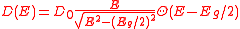
where the density of states at the channel D(E), USF, and UDF are defined as


The term, is 1 when the value inside the bracket is positive and 0 when negative. VSC is the self-consistent voltage that illustrates that the CNT energy is affected by external terminal voltages and is implicitly related to the device terminal voltages and charges at terminal capacitances by the following nonlinear equation:
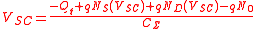
where Qt represents the charge stored in terminal capacitances, and the total terminal capacitance CΣ is the sum of the gate, drain, source, and substrate capacitances shown in the figure above. The standard approach to the solution to the self-consistent voltage equation is to use the Newton-Raphson iterative method. According to the CNT ballistic transport theory, the drain current caused by the transport of the nonequilibrium charge across the nanotube can be calculated using the Fermi–Dirac statistics.
Here F0 represents the Fermi–Dirac integral of order 0, k is the Boltzmann’s constant, T is the temperature, and ℏ the reduced Planck’s constant. This equation can be solved easily as long as the self-consistent voltage is known. However the calculation could be time-consuming when it needs to solve the self-consistent voltage with the iterative method, and this is the main drawback of this calculation.
s in their performances. In a planar gate structure, the p-CNTFET produces ~1500 A/m of the on-current per unit width at a gate overdrive of 0.6 V while p-MOSFET produces ~500 A/m at the same gate voltage. This on-current advantage comes from the high gate capacitance and improved channel transport. Since an effective gate capacitance per unit width of CNTFET is about double that of p-MOSFET, the compatibility with high- k gate dielectrics becomes a definite advantage for CNTFETs. About twice higher carrier velocity of CNTFETs than MOSFETs comes from the increased mobility and the band structure. CNTFETs, in addition, have about four times higher transconductance.
This reliability issue has been studied, and it is noticed that the multi-channeld structure can improve the reliability of the CNTFET. The multi-channeled CNTFETs can keep a stable performance after several months, while the single-channeled CNTFETs are usually out of work after a few weeks in the ambient atmosphere. The multi-channeled CNTFETs keep operating when some channels break down, this won’t happen in the single-channeled ones.
Field-effect transistor
The field-effect transistor is a transistor that relies on an electric field to control the shape and hence the conductivity of a channel of one type of charge carrier in a semiconductor material. FETs are sometimes called unipolar transistors to contrast their single-carrier-type operation with...
that utilizes a single carbon nanotube
Carbon nanotube
Carbon nanotubes are allotropes of carbon with a cylindrical nanostructure. Nanotubes have been constructed with length-to-diameter ratio of up to 132,000,000:1, significantly larger than for any other material...
or an array of carbon nanotubes as the channel material instead of bulk silicon
Silicon
Silicon is a chemical element with the symbol Si and atomic number 14. A tetravalent metalloid, it is less reactive than its chemical analog carbon, the nonmetal directly above it in the periodic table, but more reactive than germanium, the metalloid directly below it in the table...
in the traditional MOSFET
MOSFET
The metal–oxide–semiconductor field-effect transistor is a transistor used for amplifying or switching electronic signals. The basic principle of this kind of transistor was first patented by Julius Edgar Lilienfeld in 1925...
structure. Since it was first demonstrated in 1998, there have been tremendous developments in CNTFETs, which promise for an alternative material to replace silicon in future electronics.
Introduction and background
According to Moore's lawMoore's Law
Moore's law describes a long-term trend in the history of computing hardware: the number of transistors that can be placed inexpensively on an integrated circuit doubles approximately every two years....
, the dimensions of individual devices in an integrated circuit have been decreased by a factor of approximately two every two years. This scaling down of devices has been the driving force in technological advances since late 20th century. However, as noted by ITRS 2009 edition, further scaling down has faced serious limits related to fabrication technology and device performances as the critical dimension shrunk down to sub-22 nm range. The limits involve electron tunneling through short channels and thin insulator films, the associated leakage currents, passive power dissipation, short channel effects, and variations in device structure and doping. These limits can be overcome to some extent and facilitate further scaling down of device dimensions by modifying the channel material in the traditional bulk MOSFET structure with a single carbon nanotube or an array of carbon nanotubes.
Electronic structure of carbon nanotubes
The exceptional electrical properties of carbon nanotubes arise from the unique electronic structure of graphene itself that can roll up and form a hollow cylinder. The circumference of such carbon nanotube can be expressed in terms of a chiral vector:Ĉh=nâ1+mâ2
which connects two crystallographically equivalent sites of the two-dimensional graphene sheet. Here n and m are integers and â1 and â2 are the unit vectors of the hexagonal honeycomb lattice. Therefore, the structure of any carbon nanotube can be described by an index with a pair of integers (n,m) that define its chiral vector.
In terms of the integers (n,m), the nanotube diameter dt is given by:
and the chiral angle θ is given by:
-
 .
.
The differences in the chiral angle and the diameter cause the differences in the properties of the various carbon nanotubes. For example, it can be shown that an (n,m) carbon nanotube is metallic when n = m, has a small gap when n – m = 3i, where i is an integer, and is semiconducting when n – m ≠ 3i. This is due to the fact that the periodic boundary conditions for the one-dimensinal carbon nanotubes permit only a few wave vectors to exist around the circumference of carbon nanotubes. Metallic conduction occurs when one of these wave vectors passes through the K-point of graphene’s 2D hexagonal Brillouin zone
Brillouin zone
In mathematics and solid state physics, the first Brillouin zone is a uniquely defined primitive cell in reciprocal space. The boundaries of this cell are given by planes related to points on the reciprocal lattice. It is found by the same method as for the Wigner–Seitz cell in the Bravais lattice...
, where the valence and conduction bands are degenerate. For the semiconducting carbon nanotubes, there is a diameter dependency on bangap. For example, according to a single-particle tight-binding description of the electronic structure,
where γ is the hopping matrix element, and a is the carbon-carbon bond distance.
Motivations for transistor applications
A carbon nanotube’s bandgap is directly affected by its chirality and diameter. If those properties can be controlled, CNTs would be a promising candidate for future nano-scale transistor devices. Moreover, because of the lack of boundaries in the perfect and hollow cylinder structure of CNTs, there is no boundary scattering. CNTs are also quasi-1D materials in which only forward scattering and back scattering are allowed, and elastic scattering mean free paths in carbon nanotubes are long, typically on the order of micrometers. As a result, quasi-ballistic transport can be observed in nanotubes at relatively long lengths and low fields.Because of the strong covalent carbon-carbon bonding in the sp2 configuration, carbon nanotubes are chemically inert and are able to transport large amounts of electric current. In theory, carbon nanotubes are also able to conduct heat nearly as well as diamond or sapphire, and because of their miniaturized dimensions, the CNTFET should switch reliably using much less power than a silicon-based device.
Device fabrication
There are many types of CNTFET devices; a general survey of the most common geometries are covered below.Back-gated CNTFETs
The earliest techniques for fabricating carbon nanotube (CNT) field-effect transistors involved pre-patterning parallel strips of metal across a silicon dioxide substrate, and then depositing the CNTs on top in a random pattern. The semiconducting CNTs that happened to fall across two metal strips meet all the requirements necessary for a rudimentary field-effect transistor. One metal strip is the “source” contact while the other is the “drain” contact. The silicon oxide substrate can be used as the gate oxide and adding a metal contact on the back makes the semiconducting CNT gateable.This technique suffered from several drawbacks, which made for non-optimized transistors. The first was the metal contact, which actually had very little contact to the CNT, since the nanotube just lay on top of it and the contact area was therefore very small. Also, due to the semiconducting nature of the CNT, a Schottkey Barrier forms at the metal-semiconductor interface, increasing the contact resistance. The second drawback was due to the back-gate device geometry. Its thickness made it difficult to switch the devices on and off using low voltages, and the fabrication process led to poor contact between the gate dielectric and CNT.
Top-gated CNTFETs
Eventually, researchers migrated from the back-gate approach to a more advanced top-gate fabrication process. In the first step, single-walled carbon nanotubes are solution deposited onto a silicon oxide substrate. Individual nanotubes are then located via atomic force microscope or scanning electron microscope. After an individual tube is isolated, source and drain contacts are defined and patterned using high resolution electron beam lithography. A high temperature anneal step reduces the contact resistance by improving adhesion between the contacts and CNT. A thin top-gate dielectric is then deposited on top of the nanotube, either via evaporation or atomic layer deposition. Finally, the top gate contact is deposited on the gate dielectric, completing the process.Arrays of top-gated CNTFETs can be fabricated on the same wafer, since the gate contacts are electrically isolated from each other, unlike in the back-gated case. Also, due to the thinness of the gate dielectric, a larger electric field can be generated with respect to the nanotube using a lower gate voltage. These advantages mean top-gated devices are generally preferred over back-gated CNTFETs, despite their more complex fabrication process.
Wrap-around gate CNTFETs
Wrap-around gate CNTFETs, also known as gate-all-around CNTFETs were developed in 2008, and are a further improvement upon the top-gate device geometry. In this device, instead of gating just the part of the CNT that is closer to the metal gate contact, the entire circumference of the nanotube is gated. This should ideally improve the electrical performance of the CNTFET, reducing leakage current and improving the device on/off ratio.Device fabrication begins by first wrapping CNTs in a gate dielectric and gate contact via atomic layer deposition. These wrapped nanotubes are then solution-deposited on an insulating substrate, where the wrappings are partially etched off, exposing the ends of the nanotube. The source, drain, and gate contacts are then deposited onto the CNT ends and the metallic outer gate wrapping.
Suspended CNTFETs
Yet another CNTFET device geometry involves suspending the nanotube over a trench to reduce contact with the substrate and gate oxide. This technique has the advantage of reduced scattering at the CNT-substrate interface, improving device performance. There are many methods used to fabricate suspended CNTFETs, ranging from growing them over trenches using catalyst particles, transferring them onto a substrate and then under-etching the dielectric beneath, and transfer-printing onto a trenched substrate.The main problem suffered by suspended CNTFETs is that they have very limited material options for use as a gate dielectric (generally air or vacuum), and applying a gate bias has the effect of pulling the nanotube closer to the gate, which places an upper limit on how much the nanotube can be gated. This technique will also only work for shorter nanotubes, as longer tubes will flex in the middle and droop towards the gate, possibly making touching the metal contact and shorting the device. In general, suspended CNTFETs are not practical for commercial applications, but they can be useful for studying the intrinsic properties of clean nanotubes.
CNTFET material considerations
There are general decisions one must make when considering what materials to use when fabricating a CNTFET. Semiconducting single-walled carbon nanotubes are preferred over metallic single-walled and metallic multi-walled tubes since they are able to be fully switched off, at least for low source/drain biases. A lot of work has been put into finding a suitable contact material for semiconducting CNTs; the best material to date is Pd, as its work function matches closely with that of nanotubes and it adheres to the CNTs quite well.I-V characteristics
In CNT-metal contacts, the different work functions of the metal and the CNT result in the Schottky barrierSchottky barrier
A Schottky barrier, named after Walter H. Schottky, is a potential barrier formed at a metal–semiconductor junction which has rectifying characteristics, suitable for use as a diode...
at the source and drain, which are made of metals like Au, Ti, Pd and Al. Even though like Schottky barrier diodes, the barriers would have made this FET to transport only one type of carrier, the carrier transport through the metal-CNT interface is dominated by quantum mechanical tunneling through the Schottky barrier. CNTFETs can easily be thinned by the gate field such that tunneling through them results in a substantial current contribution. CNTFETs are ambipolar; either electrons or holes, or both electrons and holes can be injected simultaneously. This makes the thickness of the Schottky barrier a critical factor.
CNTFETs conduct electrons when a positive bias is applied to the gate and holes when a negative bias is applied, and drain current increases with increasing a magnitude of an applied gate voltage. Around Vg = Vds/2, the current gets the minimum due to the same amount of the electron and hole contributions to the current.
Like other FETs, the drain current increases with an increasing drain bias unless the applied gate voltage is below the threshold voltage. For planar CNTFETs with different design parameters, the FET with a shorter channel length produces a higher saturation current, and the saturation drain current becomes also higher for the one consisting of smaller diameter keeping the length constant. For cylindrical CNTFETs, it is clear that a higher drain current is driven than that of planar CNTFETs since a CNT is surrounded by an oxide layer which is finally surrounded by a metal contact serving as the gate terminal.
Theoretical derivation of drain current
Theoretical investigation on drain current of the top-gate CNT transistor has been done by T.Kazierski et al.. When an electric field is applied to a CNT transistor, a mobile charge is induced in the tube from the source and drain. These charges are from the density of positive velocity states filled by the source NS and that of negative velocity states filled by the drain ND, and these densities are determined by the Fermi-Dirac probability distributions.and the equilibrium electron density is
.where the density of states at the channel D(E), USF, and UDF are defined as
The term,
is 1 when the value inside the bracket is positive and 0 when negative. VSC is the self-consistent voltage that illustrates that the CNT energy is affected by external terminal voltages and is implicitly related to the device terminal voltages and charges at terminal capacitances by the following nonlinear equation:where Qt represents the charge stored in terminal capacitances, and the total terminal capacitance CΣ is the sum of the gate, drain, source, and substrate capacitances shown in the figure above. The standard approach to the solution to the self-consistent voltage equation is to use the Newton-Raphson iterative method. According to the CNT ballistic transport theory, the drain current caused by the transport of the nonequilibrium charge across the nanotube can be calculated using the Fermi–Dirac statistics.
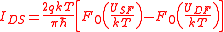
Here F0 represents the Fermi–Dirac integral of order 0, k is the Boltzmann’s constant, T is the temperature, and ℏ the reduced Planck’s constant. This equation can be solved easily as long as the self-consistent voltage is known. However the calculation could be time-consuming when it needs to solve the self-consistent voltage with the iterative method, and this is the main drawback of this calculation.
Comparison to MOSFETs
CNTFETs show different characteristics compared to MOSFETMOSFET
The metal–oxide–semiconductor field-effect transistor is a transistor used for amplifying or switching electronic signals. The basic principle of this kind of transistor was first patented by Julius Edgar Lilienfeld in 1925...
s in their performances. In a planar gate structure, the p-CNTFET produces ~1500 A/m of the on-current per unit width at a gate overdrive of 0.6 V while p-MOSFET produces ~500 A/m at the same gate voltage. This on-current advantage comes from the high gate capacitance and improved channel transport. Since an effective gate capacitance per unit width of CNTFET is about double that of p-MOSFET, the compatibility with high- k gate dielectrics becomes a definite advantage for CNTFETs. About twice higher carrier velocity of CNTFETs than MOSFETs comes from the increased mobility and the band structure. CNTFETs, in addition, have about four times higher transconductance.
Heat dissipation
The decrease of the current and burning of the CNT can occur due to the temperature raised by several hundreds of kelvins. Generally, the self-heating effect is much less severe in a semiconducting CNTFET than in a metallic one due to different heat dissipation mechanisms. A small fraction of the heat generated in the CNTFET is dissipated through the channel. The heat is non-uniformly distributed, and the highest values appear at the source and drain sides of the channel. Therefore, the temperature significantly gets lowered near the source and drain regions. For semiconducting CNT, the temperature rise has a relatively small effect on the I-V characteristics compared to silicon.Lifetime (degradation)
The carbon nanotube degrades in a few days when exposed to oxygen. There has been several works done on passivating the nanotubes with different polymers and increasing their lifetime.Reliability
Carbon nanotubes have shown reliability issues when operated under high electric field or temperature gradients. Avalanche breakdown occurs in semiconducting CNT and joule breakdown in metallic CNT. Unlike avalanche behavior in silicon, avalanche in CNTs is negligibly temperature-dependent. Applying high voltages beyond avalanche point results in Joule heating and eventual breakdown in CNTs.This reliability issue has been studied, and it is noticed that the multi-channeld structure can improve the reliability of the CNTFET. The multi-channeled CNTFETs can keep a stable performance after several months, while the single-channeled CNTFETs are usually out of work after a few weeks in the ambient atmosphere. The multi-channeled CNTFETs keep operating when some channels break down, this won’t happen in the single-channeled ones.