

Extreme ultraviolet lithography
Encyclopedia
Next-generation lithography
Next-generation lithography is a term used in integrated circuit manufacturing to describe the lithography technologies slated to replace photolithography. As of 2009 the most advanced form of photolithography is immersion lithography, in which water is used as an immersion medium for the final...
technology using an extreme ultraviolet
Extreme ultraviolet
Extreme Ultraviolet radiation is high-energy ultraviolet radiation, generally defined to be electromagnetic radiation in the part of the electromagnetic spectrum spanning wavelengths from 120 nm down to 10 nm, and therefore having photons with energies from 10 eV up to 124 eV...
(EUV) wavelength, currently expected to be 13.5 nm.
EUVL light source
Neutral atoms or condensed matter cannot emit EUV radiation. IonizationIonization
Ionization is the process of converting an atom or molecule into an ion by adding or removing charged particles such as electrons or other ions. This is often confused with dissociation. A substance may dissociate without necessarily producing ions. As an example, the molecules of table sugar...
must take place first. EUV light can only be emitted by electrons which are bound to multicharged positive ions; for example, to remove an electron from a +3 charged carbon ion (three electrons already removed) requires about 65 eV
Electronvolt
In physics, the electron volt is a unit of energy equal to approximately joule . By definition, it is equal to the amount of kinetic energy gained by a single unbound electron when it accelerates through an electric potential difference of one volt...
.
Such electrons are morei tightly bound than typical valence electrons. The existence of multicharged positive ions is only possible in a hot dense plasma
Plasma (physics)
In physics and chemistry, plasma is a state of matter similar to gas in which a certain portion of the particles are ionized. Heating a gas may ionize its molecules or atoms , thus turning it into a plasma, which contains charged particles: positive ions and negative electrons or ions...
, which itself strongly absorbs EUV. The Xe or Sn plasma sources for EUV lithography are either discharge-produced or laser-produced. Power output exceeding 100 W is a requirement for sufficient throughput. While state-of-the-art 193 nm excimer laser
Excimer laser
An excimer laser is a form of ultraviolet laser which is commonly used in the production of microelectronic devices , eye surgery, and micromachining....
s offer intensities of 200 W/cm2, lasers for producing EUV-generating plasmas need to be much more intense, on the order of 1011 W/cm2.
This indicates the enormous energy burden imposed by switching from generating 193 nm light (laser output approaching 100 W) to generating EUV light (required laser or equivalent power source output exceeding 10 kW).
A further characteristic of the plasma-based EUV sources under development is that they are not even partially coherent, unlike the KrF and ArF excimer
Excimer
An excimer is a short-lived dimeric or heterodimeric molecule formed from two species, at least one of which is in an electronic excited state. Excimers are often diatomic and are composed of two atoms or molecules that would not bond if both were in the ground state. The lifetime of an excimer is...
lasers used for current optical lithography. Further power reduction (energy loss) is expected in converting incoherent sources (emitting in all possible directions at many independent wavelengths) to partially coherent (emitting in a limited range of directions within a narrow band of wavelengths) sources by filtering (unwanted wavelengths and directions). On the other hand, coherent light poses a risk of monochromatic reflection interference and mismatch of multilayer reflectance bandwidth.
As of 2008, the development tools had a throughput of 4 wafers per hour with a 120 W source. For a 100 WPH requirement, therefore, a 3 kW source would be needed, which is not available in the foreseeable future. However, EUV photon count is determined by the number of electrons generated per photon
Photon
In physics, a photon is an elementary particle, the quantum of the electromagnetic interaction and the basic unit of light and all other forms of electromagnetic radiation. It is also the force carrier for the electromagnetic force...
which are collected by a photodiode
Photodiode
A photodiode is a type of photodetector capable of converting light into either current or voltage, depending upon the mode of operation.The common, traditional solar cell used to generateelectric solar power is a large area photodiode....
; since this is essentially the highly variable secondary yield
Secondary emission
Secondary emission in physics is a phenomenon where primary incident particles of sufficient energy, when hitting a surface or passing through some material, induce the emission of secondary particles. The primary particles are often charged particles like electrons or ions. If the secondary...
of the initial photoelectron, the dose measurement will be impacted by high variability. In fact, data by Gullikson et al. indicated ~10% natural variation of the photocurrent responsivity. More recent data for silicon photodiodes remain consistent with this assessment. Calibration of the EUV dosimeter is a nontrivial unsolved issue.
The secondary electron number variability is the well-known root cause of noise in avalanche photodiodes.
EUVL optics
EUVL is a significant departure from the deep ultraviolet lithography used today. All matter absorbs EUVExtreme ultraviolet
Extreme Ultraviolet radiation is high-energy ultraviolet radiation, generally defined to be electromagnetic radiation in the part of the electromagnetic spectrum spanning wavelengths from 120 nm down to 10 nm, and therefore having photons with energies from 10 eV up to 124 eV...
radiation. Hence, EUV lithography needs to take place in a vacuum. All the optical elements, including the photomask
Photomask
A photomask is an opaque plate with holes or transparencies that allow light to shine through in a defined pattern. They are commonly used in photolithography.-Overview:...
, must make use of defect-free Mo
Molybdenum
Molybdenum , is a Group 6 chemical element with the symbol Mo and atomic number 42. The name is from Neo-Latin Molybdaenum, from Ancient Greek , meaning lead, itself proposed as a loanword from Anatolian Luvian and Lydian languages, since its ores were confused with lead ores...
/Si
Silicon
Silicon is a chemical element with the symbol Si and atomic number 14. A tetravalent metalloid, it is less reactive than its chemical analog carbon, the nonmetal directly above it in the periodic table, but more reactive than germanium, the metalloid directly below it in the table...
multilayers which act to reflect light by means of interlayer interference; any one of these mirrors will absorb around 30% of the incident light. This limitation can be avoided in maskless interference lithography
Interference lithography
Interference lithography is a technique for patterning regular arrays of fine features, without the use of complex optical systems or photomasks.-Basic principle:...
systems. However, the latter tools are restricted to producing periodic patterns only.
The pre-production EUVL systems built to date contain at least two condenser
Condenser
Condenser may refer to:*Condenser , a device or unit used to condense vapor into liquid. More specific articles on some types include:*Air coil used in HVAC refrigeration systems...
multilayer mirrors, six projection multilayer mirrors, and a multilayer object (mask). Since the optics already absorbs 96% of the available EUV light, the ideal EUV source will need to be sufficiently bright. EUV source development has focused on plasmas
Plasma (physics)
In physics and chemistry, plasma is a state of matter similar to gas in which a certain portion of the particles are ionized. Heating a gas may ionize its molecules or atoms , thus turning it into a plasma, which contains charged particles: positive ions and negative electrons or ions...
generated by laser or discharge pulses. The mirror responsible for collecting the light is directly exposed to the plasma and is therefore vulnerable to damage from the high-energy ions and other debris.
This damage associated with the high-energy process of generating EUV radiation has precluded the successful implementation of practical EUV light sources for lithography.
The wafer throughput of an EUVL exposure tool is a critical metric for manufacturing capacity. Given that EUV is a technology requiring high vacuum, the throughput is limited (aside from the source power) by the transfer of wafers into and out of the tool chamber, to a few wafers per hour.
Another aspect of the pre-production EUVL tools is the off-axis illumination
Off-axis illumination
In photolithography, off-axis illumination is an optical system setup in which the incoming light strikes the photomask at an oblique angle rather than perpendicularly to it, that is to say, the incident light is not parallel to the axis of the optical system....
(at an angle of 6 degrees) on a multilayer mask. The resulting asymmetry in the diffraction pattern causes shadowing effects which degrade the pattern fidelity.
EUVL's shorter wavelength also increases flare
Lens flare
Lens flare is the light scattered in lens systems through generally unwanted image formation mechanisms, such as internal reflection and scattering from material inhomogeneities in the lens. These mechanisms differ from the intended image formation mechanism that depends on refraction of the image...
, resulting in less than perfect image quality and increased line width roughness.
Heating per feature volume (e.g., 20 nm cube) is higher per EUV photon compared to a photon, due to higher absorption in resist. In addition, EUV lithography results in more heating due to the vacuum environment, in contrast to the water cooling environment of immersion lithography
Immersion lithography
Immersion lithography is a photolithography resolution enhancement technique for manufacturing integrated circuits that replaces the usual air gap between the final lens and the wafer surface with a liquid medium that has a refractive index greater than one. The resolution is increased by a factor...
.
Heating is also a particularly serious issue for multilayer mirrors used, because EUV is absorbed within a thin distance from the surface. The heating density is higher. As a result, water cooling is expected to be used for the high heating load; however, the resulting vibration is a concern.
A recent study by NIST and Rutgers University found that multilayer optics contamination was highly affected by the resonant structure of the EUV mirror influencing the photoelectron generation and secondary electron yield.
Since EUV is highly absorbed by all materials, even EUV optical components inside the lithography tool are susceptible to damage, mainly manifest as observable ablation.
Such damage is a new concern specific to EUV lithography, as conventional optical lithography systems use mainly transmissive components and electron beam lithography systems do not put any component in the way of electrons, although these electrons end up depositing energy in the exposed sample substrate.
EUV exposure of photoresist
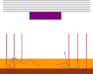
When an EUV photon is absorbed, photoelectronsPhotoelectric effect
In the photoelectric effect, electrons are emitted from matter as a consequence of their absorption of energy from electromagnetic radiation of very short wavelength, such as visible or ultraviolet light. Electrons emitted in this manner may be referred to as photoelectrons...
and secondary electrons
Secondary electrons
Secondary electrons are electrons generated as ionization products. They are called 'secondary' because they are generated by other radiation . This radiation can be in the form of ions, electrons, or photons with sufficiently high energy, i.e. exceeding the ionization potential...
are generated by ionization
Ionization
Ionization is the process of converting an atom or molecule into an ion by adding or removing charged particles such as electrons or other ions. This is often confused with dissociation. A substance may dissociate without necessarily producing ions. As an example, the molecules of table sugar...
, much like what happens when X-rays or electron beams are absorbed by matter. It has been estimated that about 4 secondary electrons on average are generated for every EUV photon, although the generation volume is not definite. These secondary electrons have energies of a few to tens of eV and travel tens of nanometers inside photoresist
Photoresist
A photoresist is a light-sensitive material used in several industrial processes, such as photolithography and photoengraving to form a patterned coating on a surface.-Tone:Photoresists are classified into two groups: positive resists and negative resists....
(see below) before initiating the desired chemical reaction. This is very similar to the photoelectron migration for the latent image
Latent image
A latent image on photographic film is an invisible image produced by the exposure of the film to light. When the film is developed, the area that was exposed darkens and forms a visible image...
formation in silver halide
Silver halide
A silver halide is one of the compounds formed between silver and one of the halogens — silver bromide , chloride , iodide , and three forms of silver fluorides. As a group, they are often referred to as the silver halides, and are often given the pseudo-chemical notation AgX...
photographic films. A contributing factor for this rather large distance is the fact that polymers have significant amounts of free volume.
In a recent actual EUV print test, it was found 30 nm spaces could not be resolved, even though the optical resolution
Optical resolution
Optical resolution describes the ability of an imaging system to resolve detail in the object that is being imaged.An imaging system may have many individual components including a lens and recording and display components...
and the photoresist composition were not the limiting factor.
In particular, for photoresists utilizing chemical amplification for higher throughput:
e- + acid generator -> anion -> dissociated anion products
This reaction, also known as "electron attachment" or "dissociative electron attachment" is most likely to occur after the electron has essentially slowed to a halt, since it is easiest to capture at that point. The cross-section for electron attachment is inversely proportional to electron energy at high energies, but approaches a maximum limiting value at zero energy. On the other hand, it is already known that the mean free path at the lowest energies (few to several eV or less, where dissociative attachment is significant) is well over 10 nm, thus limiting the ability to consistently achieve resolution at this scale. In addition, electrons with energies < 20 eV are capable of desorbing hydrogen and fluorine anions from the resist, leading to potential damage to the EUV optical system.
EUV photoresist images often require resist thicknesses roughly equal to the pitch. This is not only due to EUV absorption causing less light to reach the bottom of the resist but also to forward scattering from the secondary electrons (similar to low-energy electron beam lithography
Electron beam lithography
Electron beam lithography is the practice of emitting a beam of electrons in a patterned fashion across a surface covered with a film , and of selectively removing either exposed or non-exposed regions of the resist...
). Conversely, thinner resist transmits a larger fraction of incident light allowing damage to underlying films, yet requires more dosage to achieve the same level of absorption.
Since the photon absorption depth exceeds the electron escape depth, as the released electrons eventually slow down, they dissipate their energy ultimately as heat.
An EUV dose of 1 mJ/cm2 generates an equivalent photoelectron dose of 10.9 μC/cm2. Current demonstration doses exceed 10 mJ/cm2, or equivalently, 109 μC/cm2 photoelectron dose.
The use of higher doses and/or reduced resist thicknesses to produce smaller features only results in increased irradiation of the layer underneath the photoresist. This adds another significant source of photoelectrons and secondary electrons which effectively reduce the image contrast. In addition, there is increased possibility of ionizing radiation damage to the layers below.
The extent of secondary electron and photoelectrons in blurring the resolution is dependent on factors such as dose, surface contamination, temperature, etc.
EUVL defects
EUVL faces specific defect issues analogous to those being encountered by immersion lithographyImmersion lithography
Immersion lithography is a photolithography resolution enhancement technique for manufacturing integrated circuits that replaces the usual air gap between the final lens and the wafer surface with a liquid medium that has a refractive index greater than one. The resolution is increased by a factor...
. Whereas the immersion-specific defects are due to unoptimized contact between the water and the photoresist, EUV-related defects are attributed to the inherently ionizing energy of EUV radiation. The first issue is positive charging, due to ejection of photoelectrons freed from the top resist surface by the EUV radiation. This could lead to electrostatic discharge or particle contamination as well as the device damage mentioned above. A second issue is contamination deposition on the resist from ambient or outgassed hydrocarbons, which results from EUV- or electron-driven reactions.
A third issue is etching of the resist by oxygen, argon or other ambient gases, which have been dissociated by the EUV radiation or the electrons generated by EUV. Ambient gases in the lithography chamber may be used for purging and contamination reduction. These gases are ionized by EUV radiation, leading to plasma generation in the vicinity of exposed surfaces, resulting in damage to the multilayer optics and inadvertent exposure of the sample.
The phase shift caused by an undetected 3 nm mask substrate flatness variation is sufficient to produce a printable defect. The principle behind this is a quarter-wavelength deviation from the flat surface produces a half-wavelength optical path difference after reflection. The light that is reflected from the flat surface is 180 degrees out of phase with the light reflected from the quarter-wavelength deviation.
It has been shown that even a 1 nm deviation from flatness would lead to a substantial reduction (~20%) of the image intensity.
In fact, defects of atomic scale height (0.3-0.5 nm) with 100 nm FWHM
Full width at half maximum
Full width at half maximum is an expression of the extent of a function, given by the difference between the two extreme values of the independent variable at which the dependent variable is equal to half of its maximum value....
can still be printable by exhibiting 10% CD impact.
Like a lens
Lens (optics)
A lens is an optical device with perfect or approximate axial symmetry which transmits and refracts light, converging or diverging the beam. A simple lens consists of a single optical element...
, any defect which effectively produces a phase shift scatters light outside the defect region. The amount of light that is scattered can be calculated.
Furthermore, the edge of a phase defect will further reduce reflectivity by more than 10% if its deviation from flatness exceeds 3 degrees, due to the deviation from the target angle of incidence of 84 degrees with respect to the surface. Even if the defect height is shallow, the edge still deforms the overlying multilayer, producing an extended region where the multilayer is sloped. The more abrupt the deformation, the narrower the defect edge extension, the greater the loss in reflectivity.
Unexpected resolution limits
Given that EUV is a significant reduction in wavelength compared to current lithography wavelengths, one would expect significantly better resolution. However, the resolution is ultimately determined by the interaction volume in the image recording medium, i.e., the photoresist. As noted above, the low energy electrons released by EUV could blur the original EUV image. In addition, there are statistical effects, especially for feature areas less than 1500 square nanometers.Resist Polymer Aggregates
Resists as polymers are well-known to have aggregates with sizes up to 80 nm. Even the high-resolution resist HSQ has aggregate size reduced down to only 15–20 nm.While the roughness of lines larger than the aggregate size are mildly affected by the aggregate size, below the aggregate size obviously the linewidth can be severely affected.
Shot noise
The required dose sensitivity of 5 mJ/cm2 implies only several thousand EUV photons or so accumulate in such a small area. With the natural Poisson distributionPoisson distribution
In probability theory and statistics, the Poisson distribution is a discrete probability distribution that expresses the probability of a given number of events occurring in a fixed interval of time and/or space if these events occur with a known average rate and independently of the time since...
due to the random arrival times of the photons, there is an expected natural dose variation of at least a few percent 3 sigma, making the exposure process fundamentally uncontrollable for features less than about 40 nm. Increasing the dose will reduce the shot noise, but will also increase the flare dose and generate more free electrons. The free electrons will spread out before slowing to a stop. Since the free electron density is lower than the initial photon density, the shot noise is always effectively larger than expected from just considering the EUV dose.
Intel recently calculated that for printing one billion 30 nm contacts, +/- 16% dose error (@10 mJ/cm2) is expected from the EUV shot noise. With acid counting, the fluctuation increases to +/- 20%. This issue will affect 22 nm patterning integration. When one considers that within a 1 nm pixel, the shot noise is even more significant (>100% on 10 nm scale @10 mJ/cm2), the origin of the line edge roughness (LER) issue in EUV lithography becomes clearer.
The 2D patterns often encountered in DRAM and logic microprocessors (including multiple pattern cutting for 11 nm node) as well as the floating gate flash memory
Flash memory
Flash memory is a non-volatile computer storage chip that can be electrically erased and reprogrammed. It was developed from EEPROM and must be erased in fairly large blocks before these can be rewritten with new data...
patterns with 2D isolation for charge trapping are more susceptible to shot noise than line-type features. It is because the 2D pattern (ideally rectangular) is defined by the number of photons in a limited area exposed above or below a certain threshold dose.
| Dose (mJ/cm2) | Photons/nm2 | No. of photons in 25 nm diameter | 6s/avg dose noise (30% absorbed) |
|---|---|---|---|
| 5 | 3.4 | 1667 | 26.8% |
| 10 | 6.8 | 3335 | 19.0% |
| 15 | 10.2 | 5002 | 15.5% |
| 20 | 13.6 | 6669 | 13.4% |
| 25 | 17.0 | 8337 | 12.0% |
Note: 1–10 ppb of population is about 6 standard deviations away from the mean dose.
Ref.: EUV resist TWG 2008
The shot noise issue is also applicable to the features patterned on masks used for EUV, targeted at 20 nm and below.
A 12 uC/cm2 absorbed dose used to pattern 80 nm contact holes on a mask (to print 20 nm on wafer) inevitably experiences 10% shot noise in the dose level over the population of a billion such contact holes.
Proximity effect (secondary electrons)
It is now recognized that for insulating materials like PMMA, low energy electrons can travel quite a far distance (several nanometre is possible). This is due to the fact that below the ionization potentialIonization potential
The ionization energy of a chemical species, i.e. an atom or molecule, is the energy required to remove an electron from the species to a practically infinite distance. Large atoms or molecules have a low ionization energy, while small molecules tend to have higher ionization energies.The property...
the only energy loss mechanism is mainly through phonon
Phonon
In physics, a phonon is a collective excitation in a periodic, elastic arrangement of atoms or molecules in condensed matter, such as solids and some liquids...
s and polaron
Polaron
A polaron is a quasiparticle composed of a charge and its accompanying polarization field. A slow moving electron in a dielectric crystal, interacting with lattice ions through long-range forces will permanently be surrounded by a region of lattice polarization and deformation caused by the moving...
s.
It should be noted that polaronic effects are manifest more strongly in ionic crystals than polymers. In fact, polaron hopping could extend as far as 20 nm.
Adding a worst case of ~20 nm broadening to an expected EUV tool resolution of ~10 nm, we expect the practical effective resolution to be at best ~30 nm, which is comparable to state-of-the-art immersion lithography with current double patterning
Double patterning
Multiple patterning is a class of technologies for manufacturing integrated circuits , developed for photolithography to enhance the feature density. The simplest case of multiple patterning is double patterning, where a conventional lithography process is enhanced to produce double the expected...
lithography. Allowing 20 nm electron range to be only 10% of the critical dimension as variability, automatically challenges sub-200 nm lithography.
In a classic experiment by Feder et al. at IBM
IBM
International Business Machines Corporation or IBM is an American multinational technology and consulting corporation headquartered in Armonk, New York, United States. IBM manufactures and sells computer hardware and software, and it offers infrastructure, hosting and consulting services in areas...
, an erbium
Erbium
Erbium is a chemical element in the lanthanide series, with the symbol Er and atomic number 68. A silvery-white solid metal when artificially isolated, natural erbium is always found in chemical combination with other elements on Earth...
layer on a PMMA resist layer was exposed to X-rays. The erbium layer absorbed the X-rays strongly, producing low energy secondary electrons. The X-rays which were not absorbed continued to penetrate into the PMMA, where they were only lightly absorbed. Upon removal of the erbium layer and subsequent PMMA development in solvent, the resist removal rate was found to be accelerated for the top 40 nm of the PMMA film, while it was much more gradual for the rest of the film. The accelerated rate was due to the secondary electron exposure, while the gradual rate was due to the X-ray absorption. This proved the maximum secondary electron exposure range of 40 nm in this case.
A more recent experiment was performed by Carter et al. at MIT
Massachusetts Institute of Technology
The Massachusetts Institute of Technology is a private research university located in Cambridge, Massachusetts. MIT has five schools and one college, containing a total of 32 academic departments, with a strong emphasis on scientific and technological education and research.Founded in 1861 in...
and University of Wisconsin–Madison
University of Wisconsin–Madison
The University of Wisconsin–Madison is a public research university located in Madison, Wisconsin, United States. Founded in 1848, UW–Madison is the flagship campus of the University of Wisconsin System. It became a land-grant institution in 1866...
, where the X-ray absorber generating the electrons was beneath the PMMA resist rather than on top of it. In this case, the accelerated dissolution of PMMA started approximately 50 nm above the substrate.
The significance of this secondary electron range is the appearance of a "proximity effect
Proximity effect (electron beam lithography)
The proximity effect in electron beam lithography is the phenomenon that the exposure dose distribution, and hence the developed pattern, is wider than the scanned pattern, due to the interactions of the primary beam electrons with the resist and substrate...
" for distances on the order of 50 nm or less.
This causes the exposure tolerance to be reduced dramatically as feature sizes decrease below this range. Even though features can still print below this range, the resolution is affected by the randomness of energy distribution. The difference in experimentally determined ranges above (40 nm vs. 50 nm) is an indication of this fundamental variability. The secondary electron exposure can also be thought of as a blur effect. The blur is generally not included in optical-only image simulations.
The proximity effect is also manifest by photoelectrons and secondary electrons leaving the top surface of the resist and then returning some tens of nanometers distance away.
This also can be understood in terms of the emitted electrons forming a space charge
Space charge
Space charge is a concept in which excess electric charge is treated as a continuum of charge distributed over a region of space rather than distinct point-like charges...
cloud above the surface which is attracted to the positively charged surface in the vertical direction but laterally disperses (in vacuum) due to the negative charge mutual repulsion.
The secondary electron proximity effect was recently demonstrated by Stanford University using a scanning probe tip that emitted electrons in the 40–60 eV energy range. Dose sensitivity was demonstrated more than 25 nm away from the exposure center. It indicates that within a 50 nm range of exposure widths, the low-energy (EUV-generated) electron distribution influences the linewidth distribution. This is a new effect not seen with conventional optical lithography.
Photoelectron emission microscopy (PEEM) data was used to show that low energy electrons ~1.35 eV could travel as far as ~15 nm in SiO2, despite an average measured attenuation length of 1.18 nm.
Photoelectron trajectories
Kotera et al. performed EUV photoelectron trajectory simulations, showing their range to be 30 nm.The spread of the energy deposition by these electrons can account for the observed line edge roughness. The top layer exposure is effectively less because electrons emitted from the surface never come back.
Efficient photoresist heating
Ritucci et al., reported on the improved thermal ablation efficiency for EUV wavelengths compared to DUV wavelengths.Since EUV exceeds the bandgap of all materials, it is more easily absorbed than longer wavelengths, and the same dose of incident energy results in more heating; even ~100 mJ/cm2 would be hot enough to result in ablation. The resolution of chemically amplified photoresists is determined by thermally driven acid diffusion (spreading). It is worth noting that even at the ablation dose of 100 mJ/cm2, the shot noise for a 1 nm pixel is still significant (3σ/avg = 36%), which could severely impact a critical dimension (CD) for which the pixel is at least 5%, i.e., 20 nm or less.
Point spread function of resist
Kozawa et al. determined the point spread function of EUV chemically amplified resists using a basic acid generation calculation and simulation fit. The range of acid generation extended ~20 nm from the absorption point, entailing a ~40 nm resolution limit.Given that photoresists easily diffuse acid molecules, it would be no surprise that the smaller and lighter electrons produced by EUV or other ionizing radiation would diffuse faster and further, rendering the expected optical resolution meaningless.
The resist blur based on print results at the end of 2008 is in the range of 10-16 nm. Half-pitch resolution is still a struggle below 30 nm, and line edge roughness is still a major issue.
Uncertainty principle
As secondary electron generation involves inelastic scattering with momentum transfer, there will be an associated position uncertainty. As lower energy electrons have less momentum transfer, the delocalization of the secondary electron generation process tends to be higher (~nm), which would have a more direct impact on LER.EUVL demonstrations
Interference lithography at the Paul Scherrer InstitutePaul Scherrer Institute
The Paul Scherrer Institute is a multi-disciplinary research institute which belongs to the Swiss ETH-Komplex covering also the ETH Zurich and EPFL...
has been used to demonstrate sub-20 nm line-space features. However, it must be kept in mind a range of ultraviolet
Ultraviolet
Ultraviolet light is electromagnetic radiation with a wavelength shorter than that of visible light, but longer than X-rays, in the range 10 nm to 400 nm, and energies from 3 eV to 124 eV...
and X-ray
X-ray
X-radiation is a form of electromagnetic radiation. X-rays have a wavelength in the range of 0.01 to 10 nanometers, corresponding to frequencies in the range 30 petahertz to 30 exahertz and energies in the range 120 eV to 120 keV. They are shorter in wavelength than UV rays and longer than gamma...
wavelengths corresponding to the photon energy range 10–135 eV are included in the synchrotron light spectrum that is used as the source.
The resist performance tested with this source therefore does not reflect the performance expected for an EUV projection tool.
In 1996, a collaboration between Sandia National Laboratories, University of California at Berkeley, and Lucent Technologies, produced NMOS transistors with gate lengths from 75 nm to 180 nm. The gate lengths were defined by EUV lithography.
The device saturation current at 130 nm gate length was ~0.2 mA/um. A 100 nm gate device showed subthreshold swing of 90 mV/decade and saturated transconductance of 250 mS/mm. A commercial NMOS at the same design rule patterned by then-state-of-the-art DUV lithography showed 0.94 mA/um saturation current and 860 mS/mm saturated transconductance. The subthreshold swing in this case was less than 90 mV/decade.
In February 2008, a collaboration including IBM
IBM
International Business Machines Corporation or IBM is an American multinational technology and consulting corporation headquartered in Armonk, New York, United States. IBM manufactures and sells computer hardware and software, and it offers infrastructure, hosting and consulting services in areas...
and AMD
Advanced Micro Devices
Advanced Micro Devices, Inc. or AMD is an American multinational semiconductor company based in Sunnyvale, California, that develops computer processors and related technologies for commercial and consumer markets...
, based at the College of Nanoscale Science and Engineering (CNSE) in Albany, New York, used EUV lithography to pattern 90 nm trenches in the first metal layer of a 45 nm node test chip.
No specific details on device performance were given. However, the lithographic performance details given still indicated much to be desired:
- CD uniformity: 6.6%
- Overlay: 17.9 nm x, 15.6 nm y, possibly correctable to 6.7 nm x, 5.9 nm y
- Power: 1 W at wafer (>200 W required for high volume), with a dose of 3.75 mJ/cm2
- Defects: 1/sq. cm.
The high defect level may not be unexpected as AMD's 45 nm node Metal 1 design rule was 90 nm while the same EUV exposure theoretically could result in printed defects below 30 nm originating from mask defects larger than 100 nm. Optical lithography pushed beyond its natural resolution limit has a significant advantage in this regard.
Apparently, the CNSE EUV tool suffered from a well-known 16% flare problem.
Flare effects may be difficult to separate from the secondary electron effects discussed earlier.
Also in July 2008, IMEC
Imec
Imec is a micro- and nanoelectronics research center headquartered in Leuven, Belgium, with offices in Belgium, the Netherlands, Taiwan, USA, China and Japan. Its staff of about 1,900 people includes more than 500 industrial residents and guest researchers...
printed ~60 nm contacts using their installed EUV tool.
Doses of 12–18 mJ/cm2 were used.
In August 2008, SEMATECH
SEMATECH
- Purpose :SEMATECH , a not-for-profit consortium, performs research and development to advance chip manufacturing. SEMATECH has broad engagement with various sectors of the R&D community, including chipmakers, equipment and material suppliers, universities, research institutes, and government...
demonstrated a 22 nm half-pitch using chemically-amplified photoresist. However, even at 15 mJ/cm2, the linewidth roughness was very significant, 5–6 nm, so that even the image pitch regularity was challenged.
In April 2009, IMEC fabricated 22 nm SRAM cells where the contact and Metal 1 layers (~45 nm design rule) were printed with EUV lithography.
However, it was acknowledged that EUV would not be ready when companies start using 22 nm. In addition, it was commented that the feature edge profiles indicated slope asymmetry related to the characteristic EUV illumination asymmetry. Whereas this demonstration only focused on a limited number of ~45 nm features, Intel's shot noise calculation above for billions of features ~30 nm indicates difficult challenges ahead for manufacturing.
In late 2009, KLA-Tencor and GlobalFoundries along with Lawrence Berkeley National Labs published a paper which showed the stochastic behavior of EUV-generated secondary electrons in EUV resists. In particular, 32 nm half-pitch trenches showed significant edge roughness, width roughness and critical dimension (CD) variability. It may also explain the ~ 15 nm resist blur observed in an earlier study.
Timing impact
"Good progress has been made on all the technology fronts," said Paolo Gargini, Director of Technology Strategy for Intel Corporation, in 2003. He continued, "Commercialization in 2009 remains the main goal for all the EUV community." However, as of today, EUVL still has not been commercialized.The difficulties of EUV stem mainly from the difficulty of EUV light generation and the sensitivity of EUV light to surface contamination and roughness.
2009
In July 2009, ASML HoldingASML Holding
ASML is a Dutch company and the largest supplier in the world of photolithography systems for the semiconductor industry. The company manufactures machines for the production of integrated circuits , such as RAM and flash memory chips and CPUs.-Products:...
and Cymer Inc. announced the shipment of the first fully integrated laser-produced plasma (LPP) extreme ultraviolet (EUV) lithography light source from Cymer to ASML, where it is supporting integration and testing of next generation EUV lithography scanners.
In July 2009, a review of the EUV infrastructure indicated that there were significant gaps remaining, in particular for mask defect inspection. The gaps may not be filled until 2013 or later, which would impact the rollout of EUV for high-volume manufacturing by 2015.
It was most recently indicated that EUV mask features ~100 nm half-pitch (on the mask itself) were at the current resolution limit of EUV mask generation. Since these features would be demagnified 4X for upcoming 300 mm tools, it would indicate the mask itself would not be able to conventionally print good images at ~25 nm half-pitch or below. The same study reiterated that resolution was not limited by the optics but by the resist response, which prevented sub-20 nm half-pitch even with mask resolution enhancement. This resolution limit on the mask itself could be tied to the shot noise issue pointed out above which is involved in the fabrication of the mask.
2010
In June 2010, TSMC announced it would take delivery of an EUV system for purposes, to be delivered in 2011. The tool's weight reportedly warranted purchasing a special clamp costing more than 2 million USD.In July 2010, at Semicon West 2010, ASML
ASML Holding
ASML is a Dutch company and the largest supplier in the world of photolithography systems for the semiconductor industry. The company manufactures machines for the production of integrated circuits , such as RAM and flash memory chips and CPUs.-Products:...
updated the resolution achieved by EUVL, the status being 24 nm in 2010, but with a severely degraded NILS (normalized image log-slope) below 1.0, indicating poor lithographic quality.
In fact, as finer resolution is projected, the NILS is expected to go to 0, indicating impossibility of EUVL use.
In 2010, Samsung cited various additional processes still needed to be developed to address line-width roughness (LWR), arising from the shot noise discussed earlier, which would drive up costs.
In addition, it cited out-of-band wavelengths in the DUV range as causing flare effects; this was also observed by others.
At SPIE 2010, researchers from the Center for X-ray Optics at Lawrence Berkeley National Laboratory and the University of Berkeley presented results showing that replicated surface roughness (RSR) from the substrate to the multilayer surface as low as 50 pm could induce phase errors that are imaged as speckle with defocus, which would lead to line-edge roughness (LER) that could not be tolerated for the 22 nm and 16 nm nodes.
This spec is much smaller than current capabilities. For reference, the Bohr radius
Bohr radius
The Bohr radius is a physical constant, approximately equal to the most probable distance between the proton and electron in a hydrogen atom in its ground state. It is named after Niels Bohr, due to its role in the Bohr model of an atom...
is 53 pm and the rms surface roughness of silicon wafers is on the order of 100 pm.
ASML EUV tools in use or in development
| Available Year | EUV Tool | Resolution | Throughput | Dose, Source |
|---|---|---|---|---|
| 2006 | ADT | 32 nm | 4 WPH | 5 mJ/cm2, ~8W |
| 2010 | NXE:3100 | 27 nm | 60 WPH | 10 mJ/cm2, >100W |
| 2012 | NXE:3300B | 22 nm | 125 WPH | 15 mJ/cm2, >250W |
| 2013 | NXE:3300C | Depends on resist diffusion length | 150 WPH | 15 mJ/cm2, >350W |
Source: ASML, International Workshop on EUVL, Maui 2010
Timing for 1x nm and beyond
HynixHynix
Hynix Semiconductor Inc. chips and flash memory chips. Founded in 1983, Hynix is the world's second-largest memory chipmaker, the largest being Samsung Electronics. Formerly known as Hyundai Electronics, the company has manufacturing sites in Korea, the U.S., China and Taiwan...
has found that 193 nm immersion lithography with double patterning could resolve down to ~ 20 nm, while the more cost-conscious EUV approach could only resolve down to 28 nm, less than a generation's improvement over 193 nm immersion lithography single patterning's resolution limit of 38 nm.
Due to its current resolution limitations and lack of readiness, EUVL has recently been supplanted by multiple patterning using existing immersion lithography tools as the lithography of choice for current 20-nm class NAND Flash technology generations and beyond.
Samsung
Samsung
The Samsung Group is a South Korean multinational conglomerate corporation headquartered in Samsung Town, Seoul, South Korea...
and IM Flash Technologies
IM Flash Technologies
IM Flash Technologies, LLC is the name for the semiconductor company founded in January 2006, by Micron Technology, Inc., one of the world's leading providers of advanced semiconductor solutions, and Intel Corporation, the world’s largest chip maker....
have already started using spacer double patterning for their 3X nm and 2X nm NAND Flash. Toshiba and SanDisk are already starting to make 19 nm NAND flash in 2011. In fact, with EUV single exposure resolution still exceeding 22 nm, multiple patterning would be necessary for ~10 nm regardless of using EUV or ArF wavelength. At IEDM 2011, Hynix is expected to report on 1X nm NAND technology using quadruple spacer patterning.
In September 2009, Intel disclosed that for its 15 nm process, EUV did not appear to be ready in timely fashion.
Hence, Intel is preparing to extend 193 nm immersion lithography with double and possibly triple patterning to 15 nm.
Currently, it is also exploring the feasibility of EUV for its 11 nm logic node; however, 2D contact patterning still appears only good to ~ 26 nm half-pitch, while a special rinse for improving line width roughness appears very pitch-dependent. Intel has declared that even without EUV, it could still use 193 nm immersion lithography at the 11 nm node.
As of 2010, it has been observed that EUV would be delayed until 2015 to allow the development of the required EUV inspection tools. On the other hand, manufacturer roadmaps show 2012–2013 as the timing needed for 1x nm, precluding the use of EUV. Consideration of long-term implementation of EUVL will now need to consider sub-10 nm design rules. However, at this point, due to larger electric field vector angles, polarization effects become important.
The effective flare for 10 nm half-pitch lines-spaces due to polarization effects is 11%. The difficulty of EUV is the lack of polarization control (no laser sources, only plasmas).
ASML has indicated that below 16 nm capability would require a larger illumination angle than the current 6°, and hence require a fundamental change to the current EUV multilayer optics infrastructure.
In fact, for EUV mask pitches of 8 wavelengths or less (demagnified 4x to 2 wavelengths (13-14 nm half-pitch) or less on the wafer), diffraction into the multilayer at larger angles is another source of significant image degradation, which requires intensive computation to evaluate. For larger angles, the multilayer reflectance decreases significantly.
Another issue is that for sub-10 nm applications, the electron beam lithography
Electron beam lithography
Electron beam lithography is the practice of emitting a beam of electrons in a patterned fashion across a surface covered with a film , and of selectively removing either exposed or non-exposed regions of the resist...
for EUV mask patterning, already burdened by throughput issues, will have practical resist difficulties for meeting the resolution requirement. In fact, for 20 nm and below, the current electron-beam mask writers cannot repeatably deliver 80 nm sizes on the mask, which corresponds to 20 nm on the wafer.
Recent EUV zone plate lithography reports have indicated that for sub-20 nm half-pitch, even next-generation lithography would require double patterning; in fact, double patterning may not be sufficient even for sub-12 nm half-pitch. As a result, the overlay and throughput requirements would need to be at least twice as stringent as before.
At the 2011 LithoVision conference, Intel indicated that EUV technology is already late for even Intel's 10 nm design rule planning.
Resource requirements: EUV vs. ArF immersion double patterning
| Utility | 200 W output EUV | 90 W output ArF immersion double patterning |
|---|---|---|
| Electrical power (kW) | 532 | 49 |
| Cooling water flow (L/min) | 1600 | 75 |
| Gas lines | 6 | 3 |
Source: Gigaphoton, Sematech Symposium Japan, September 15, 2010
The required utility resources are significantly larger for EUV compared to 193 nm immersion, even with double patterning. Additionally, to confine ion debris, a superconducting magnet may be required.