
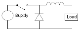
Buck converter
Encyclopedia
A buck converter is a step-down DC to DC converter
. Its design is similar to the step-up boost converter
, and like the boost converter it is a switched-mode power supply
that uses two switches (a transistor
and a diode
), an inductor and a capacitor.
The simplest way to reduce the voltage of a DC supply is to use a linear regulator
(such as a 7805), but linear regulators waste energy as they operate by dissipating excess power as heat. Buck converters, on the other hand, can be remarkably efficient (95% or higher for integrated circuits), making them useful for tasks such as converting the typical battery voltage in a laptop down to the few volts needed by the processor
.

 The operation of the buck converter is fairly simple, with an inductor
and two switches (usually a transistor
and a diode
) that control the inductor. It alternates between connecting the inductor to source voltage to store energy in the inductor and discharging the inductor into the load.
The energy stored in inductor L is

Therefore, it can be seen that the energy stored in L increases during On-time (as IL increases) and then decreases during the Off-state. L is used to transfer energy from the input to the output of the converter.
The rate of change of IL can be calculated from:

With VL equal to during the On-state and to
  during the Off-state. Therefore, the increase in current during the On-state is given by:
 , t{on}= DT
Identically, the decrease in current during the Off-state is given by:
 , t{off}= T
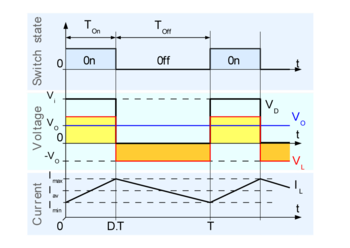
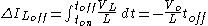
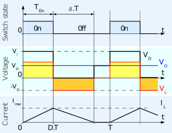
If we assume that the converter operates in steady state, the energy stored in each component at the end of a commutation cycle T is equal to that at the beginning of the cycle. That means that the current IL is the same at t=0 and at t=T (see figure 4).
So we can write from the above equations:
It is worth noting that the above integrations can be done graphically: In figure 4, is proportional to the area of the yellow surface, and
  to the area of the orange surface, as these surfaces are defined by the inductor voltage (red) curve. As these surfaces are simple rectangles, their areas can be found easily:
  for the yellow rectangle and
  for the orange one. For steady state operation, these areas must be equal.
As can be seen on figure 4, and
and  . D is a scalar called the duty cycle with a value between 0 and 1. This yields:
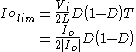
From this equation, it can be seen that the output voltage of the converter varies linearly with the duty cycle for a given input voltage. As the duty cycle D is equal to the ratio between tOn and the period T, it cannot be more than 1. Therefore, . This is why this converter is referred to as step-down converter.
So, for example, stepping 12 V down to 3 V (output voltage equal to a fourth of the input voltage) would require a duty cycle of 25%, in our theoretically ideal circuit.
 We still consider that the converter operates in steady state. Therefore, the energy in the inductor is the same at the beginning and at the end of the cycle (in the case of discontinuous mode, it is zero). This means that the average value of the inductor voltage (VL) is zero; i.e., that the area of the yellow and orange rectangles in figure 5 are the same. This yields:
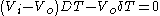
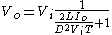
So the value of δ is:

The output current delivered to the load ( ) is constant, as we consider that the output capacitor is large enough to maintain a constant voltage across its terminals during a commutation cycle. This implies that the current flowing through the capacitor has a zero average value. Therefore, we have :

Where is the average value of the inductor current. As can be seen in figure 5, the inductor current waveform has a triangular shape. Therefore, the average value of IL can be sorted out geometrically as follow:
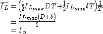
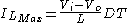
The inductor current is zero at the beginning and rises during ton up to ILmax. That means that ILmax is equal to:
Substituting the value of ILmax in the previous equation leads to:
And substituting δ by the expression given above yields:
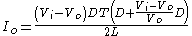
This expression can be rewritten as:
It can be seen that the output voltage of a buck converter operating in discontinuous mode is much more complicated than its counterpart of the continuous mode. Furthermore, the output voltage is now a function not only of the input voltage (Vi) and the duty cycle D, but also of the inductor value (L), the commutation period (T) and the output current (Io).
 As mentioned at the beginning of this section, the converter operates in discontinuous mode when low current is drawn by the load, and in continuous mode at higher load current levels. The limit between discontinuous and continuous modes is reached when the inductor current falls to zero exactly at the end of the commutation cycle. with the notations of figure 5, this corresponds to :
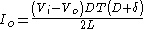
Therefore, the output current (equal to the average inductor current) at the limit between discontinuous and continuous modes is (see above):
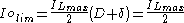
Substituting ILmax by its value:
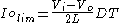
On the limit between the two modes, the output voltage obeys both the expressions given respectively in the continuous and the discontinuous sections. In particular, the former is

So Iolim can be written as:
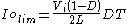
Let's now introduce two more notations:
Using these notations, we have:
DC to DC converter
A DC-to-DC converter is an electronic circuit which converts a source of direct current from one voltage level to another. It is a class of power converter.- Usage :...
. Its design is similar to the step-up boost converter
Boost converter
A boost converter is a power converter with an output DC voltage greater than its input DC voltage. It is a class of switching-mode power supply containing at least two semiconductor switches and at least one energy storage element...
, and like the boost converter it is a switched-mode power supply
Switched-mode power supply
A switched-mode power supply is an electronic power supply that incorporates a switching regulator in order to be highly efficient in the conversion of electrical power...
that uses two switches (a transistor
Transistor
A transistor is a semiconductor device used to amplify and switch electronic signals and power. It is composed of a semiconductor material with at least three terminals for connection to an external circuit. A voltage or current applied to one pair of the transistor's terminals changes the current...
and a diode
Diode
In electronics, a diode is a type of two-terminal electronic component with a nonlinear current–voltage characteristic. A semiconductor diode, the most common type today, is a crystalline piece of semiconductor material connected to two electrical terminals...
), an inductor and a capacitor.
The simplest way to reduce the voltage of a DC supply is to use a linear regulator
Linear regulator
In electronics, a linear regulator is a voltage regulator based on an active device operating in its "linear region" or passive devices like Zener diodes operated in their breakdown region...
(such as a 7805), but linear regulators waste energy as they operate by dissipating excess power as heat. Buck converters, on the other hand, can be remarkably efficient (95% or higher for integrated circuits), making them useful for tasks such as converting the typical battery voltage in a laptop down to the few volts needed by the processor
Central processing unit
The central processing unit is the portion of a computer system that carries out the instructions of a computer program, to perform the basic arithmetical, logical, and input/output operations of the system. The CPU plays a role somewhat analogous to the brain in the computer. The term has been in...
.
Theory of operation
Inductor
An inductor is a passive two-terminal electrical component used to store energy in a magnetic field. An inductor's ability to store magnetic energy is measured by its inductance, in units of henries...
and two switches (usually a transistor
Transistor
A transistor is a semiconductor device used to amplify and switch electronic signals and power. It is composed of a semiconductor material with at least three terminals for connection to an external circuit. A voltage or current applied to one pair of the transistor's terminals changes the current...
and a diode
Diode
In electronics, a diode is a type of two-terminal electronic component with a nonlinear current–voltage characteristic. A semiconductor diode, the most common type today, is a crystalline piece of semiconductor material connected to two electrical terminals...
) that control the inductor. It alternates between connecting the inductor to source voltage to store energy in the inductor and discharging the inductor into the load.
Continuous mode
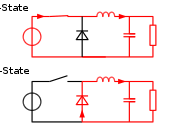
A buck converter operates in continuous mode if the current through the inductor (IL) never falls to zero during the commutation cycle. In this mode, the operating principle is described by the chronogram in figure 4:- When the switch pictured above is closed (On-state, top of figure 2), the voltage across the inductor is
 . The current through the inductor rises linearly. As the diode is reverse-biased by the voltage source V, no current flows through it;
 - When the switch is opened (off state, bottom of figure 2), the diode is forward biased. The voltage across the inductor is
 (neglecting diode drop). Current IL decreases.
The energy stored in inductor L is
Therefore, it can be seen that the energy stored in L increases during On-time (as IL increases) and then decreases during the Off-state. L is used to transfer energy from the input to the output of the converter.
The rate of change of IL can be calculated from:
With VL equal to
during the On-state and to during the Off-state. Therefore, the increase in current during the On-state is given by: , t{on}= DTIdentically, the decrease in current during the Off-state is given by:
, t{off}= TIf we assume that the converter operates in steady state, the energy stored in each component at the end of a commutation cycle T is equal to that at the beginning of the cycle. That means that the current IL is the same at t=0 and at t=T (see figure 4).
So we can write from the above equations:
It is worth noting that the above integrations can be done graphically: In figure 4,
is proportional to the area of the yellow surface, and to the area of the orange surface, as these surfaces are defined by the inductor voltage (red) curve. As these surfaces are simple rectangles, their areas can be found easily: for the yellow rectangle and for the orange one. For steady state operation, these areas must be equal.As can be seen on figure 4,
and . D is a scalar called the duty cycle with a value between 0 and 1. This yields:From this equation, it can be seen that the output voltage of the converter varies linearly with the duty cycle for a given input voltage. As the duty cycle D is equal to the ratio between tOn and the period T, it cannot be more than 1. Therefore,
. This is why this converter is referred to as step-down converter.So, for example, stepping 12 V down to 3 V (output voltage equal to a fourth of the input voltage) would require a duty cycle of 25%, in our theoretically ideal circuit.
Discontinuous mode
In some cases, the amount of energy required by the load is small enough to be transferred in a time lower than the whole commutation period. In this case, the current through the inductor falls to zero during part of the period. The only difference in the principle described above is that the inductor is completely discharged at the end of the commutation cycle (see figure 5). This has, however, some effect on the previous equations.So the value of δ is:
The output current delivered to the load (
) is constant, as we consider that the output capacitor is large enough to maintain a constant voltage across its terminals during a commutation cycle. This implies that the current flowing through the capacitor has a zero average value. Therefore, we have :Where
is the average value of the inductor current. As can be seen in figure 5, the inductor current waveform has a triangular shape. Therefore, the average value of IL can be sorted out geometrically as follow:The inductor current is zero at the beginning and rises during ton up to ILmax. That means that ILmax is equal to:
Substituting the value of ILmax in the previous equation leads to:
And substituting δ by the expression given above yields:
This expression can be rewritten as:
It can be seen that the output voltage of a buck converter operating in discontinuous mode is much more complicated than its counterpart of the continuous mode. Furthermore, the output voltage is now a function not only of the input voltage (Vi) and the duty cycle D, but also of the inductor value (L), the commutation period (T) and the output current (Io).
From discontinuous to continuous mode (and vice versa)
Therefore, the output current (equal to the average inductor current) at the limit between discontinuous and continuous modes is (see above):
Substituting ILmax by its value:
On the limit between the two modes, the output voltage obeys both the expressions given respectively in the continuous and the discontinuous sections. In particular, the former is
So Iolim can be written as:
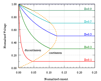
Let's now introduce two more notations:
- the normalized voltage, defined by
 . It is zero when
  , and 1 when
  ;
; - the normalized current, defined by
 . The term
  is equal to the maximum increase of the inductor current during a cycle; i.e., the increase of the inductor current with a duty cycle D=1. So, in steady state operation of the converter, this means that
  equals 0 for no output current, and 1 for the maximum current the converter can deliver.
Using these notations, we have:
- in continuous mode:
- in discontinuous mode:
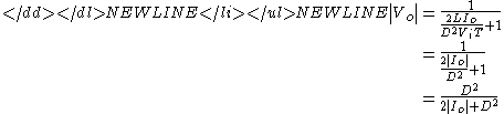
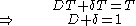
the current at the limit between continuous and discontinuous mode is:
Therefore, the locus of the limit between continuous and discontinuous modes is given by:
These expressions have been plotted in figure 6. From this, it is obvious that in continuous mode, the output voltage does only depend on the duty cycle, whereas it is far more complex in the discontinuous mode. This is important from a control point of view.
Non-ideal circuit
The previous study was conducted with the following assumptions: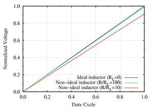
- The output capacitor has enough capacitance to supply power to the load (a simple resistance) without any noticeable variation in its voltage.
- The voltage drop across the diode when forward biased is zero
- No commutation losses in the switch nor in the diode
These assumptions can be fairly far from reality, and the imperfections of the real components can have a detrimental effect on the operation of the converter.
Output voltage ripple
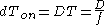
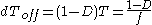
Output voltage ripple is the name given to the phenomenon where the output voltage rises during the On-state and falls during the Off-state. Several factors contribute to this including, but not limited to, switching frequency, output capacitance, inductor, load and any current limiting features of the control circuitry. At the most basic level the output voltage will rise and fall as a result of the output capacitor charging and discharging:

During the Off-state, the current in this equation is the load current. In the On-state the current is the difference between the switch current (or source current) and the load current. The duration of time (dT) is defined by the duty cycle and by the switching frequency.
For the On-state:
For the Off-state:
Qualitatively, as the output capacitor or switching frequency increase, the magnitude of the ripple decreases. Output voltage ripple is typically a design specification for the power supply and is selected based on several factors. Capacitor selection is normally determined based on cost, physical size and non-idealities of various capacitor types. Switching frequency selection is typically determined based on efficiency requirements, which tends to decrease at higher operating frequencies, as described below in Effects of non-ideality on the efficiency. Higher switching frequency can also reduce efficiency and possibly raise EMI concerns.
Output voltage ripple is one of the disadvantages of a switching power supply, and can also be a measure of its quality.
Effects of non-ideality on the efficiency
A simplified analysis of the buck converter, as described above, does not account for non-idealities of the circuit components nor does it account for the required control circuitry. Power losses due to the control circuitry is usually insignificant when compared with the losses in the power devices (switches, diodes, inductors, etc.) The non-idealities of the power devices account for the bulk of the power losses in the converter.
Both static and dynamic power losses occur in any switching regulator. Static power losses include (conduction) losses in the wires or PCB traces, as well as in the switches and inductor, as in any electrical circuit. Dynamic power losses occur as a result of switching, such as the charging and discharging of the switch gate, and are proportional to the switching frequency.
It is useful to begin by calculating the duty cycle for a non-ideal buck converter, which is:
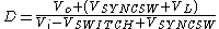
where:- VSWITCH is the voltage drop on the power switch,
- VSYNCHSW is the voltage drop on the synchronous switch or diode, and
- VL is the voltage drop on the inductor.
The voltage drops described above are all static power losses which are dependent primarily on DC current, and can therefore be easily calculated. For a transistor in saturation or a diode drop, VSWITCH and VSYNCHSW may already be known, based on the properties of the selected device.


where:
- RON is the ON-resistance of each switch (RDSON for a MOSFET), and
- RDCR is the DC resistance of the inductor.
The careful reader will note that the duty cycle equation is somewhat recursive. A rough analysis can be made by first calculating the values VSWITCH and VSYNCHSW using the ideal duty cycle equation.
Switch resistance, for components such as the power MOSFETPower MOSFETA Power MOSFET is a specific type of metal oxide semiconductor field-effect transistor designed to handle significant power levels. Compared to the other power semiconductor devices , its main advantages are high commutation speed and good efficiency at low voltages...
, and forward voltage, for components such as the insulated-gate bipolar transistor (IGBT) can be determined by referring to datasheet specifications.
In addition, power loss occurs as a result of leakage currents. This power loss is simply

where:
- ILEAKAGE is the leakage current of the switch, and
- V is the voltage across the switch.
Dynamic power losses are due to the switching behavior of the selected pass devices (MOSFETMOSFETThe metal–oxide–semiconductor field-effect transistor is a transistor used for amplifying or switching electronic signals. The basic principle of this kind of transistor was first patented by Julius Edgar Lilienfeld in 1925...
s, power transistors, IGBTs, etc.). These losses include turn-on and turn-off switching losses and switch transition losses.
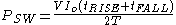
Switch turn-on and turn-off losses are easily lumped together as
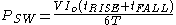
where:
- V is the voltage across the switch while the switch is off,
- tRISE and tFALL are the switch rise and fall times, and
- T is the switching period.
But this doesn't take into account the parasitic capacitance of the MOSFET which makes the Miller plate. Then, the switch losses will be more like:
When a MOSFET is used for the lower switch, additional losses may occur during the time between the turn-off of the high-side switch and the turn-on of the low-side switch, when the body diode of the low-side MOSFET conducts the output current. This time, known as the non-overlap time, prevents "shootthrough", a condition in which both switches are simultaneously turned on. The onset of shootthrough generates severe power loss and heat. Proper selection of non-overlap time must balance the risk of shootthrough with the increased power loss caused by conduction of the body diode. When a diode is used for the lower switch, diode forward turn-on time can reduce efficiency and lead to voltage overshoot.
Power loss on the body diode is also proportional to switching frequency and is

where:
- VF is the forward voltage of the body diode, and
- tNO is the selected non-overlap time.
Finally, power losses occur as a result of the power required to turn the switches on and off. For MOSFET switches, these losses are dominated by the gate charge, essentially the energy required to charge and discharge the capacitance of the MOSFET gate between the threshold voltageThreshold voltageThe threshold voltage of a MOSFET is usually defined as the gate voltage where an inversion layer forms at the interface between the insulating layer and the substrate of the transistor. The purpose of the inversion layer's forming is to allow the flow of electrons through the gate-source junction...
and the selected gate voltage. These switch transition losses occur primarily in the gate driver, and can be minimized by selecting MOSFETs with low gate charge, by driving the MOSFET gate to a lower voltage (at the cost of increased MOSFET conduction losses), or by operating at a lower frequency.

where:
- QG is the gate charge of the selected MOSFET, and
- VGS is the peak gate-source voltage.
It is essential to remember that, for N-MOSFETs, the high-side switch must be driven to a higher voltage than Vi. Therefore VG will nearly always be different for the high-side and low-side switches.
A complete design for a buck converter includes a tradeoff analysis of the various power losses. Designers balance these losses according to the expected uses of the finished design. A converter expected to have a low switching frequency does not require switches with low gate transition losses; a converter operating at a high duty cycle requires a low-side switch with low conduction losses.
Synchronous rectification
A synchronous buck converter is a modified version of the basic buck converter circuit topology in which the diode, D, is replaced by a second switch, S2. This modification is a tradeoff between increased cost and improved efficiency.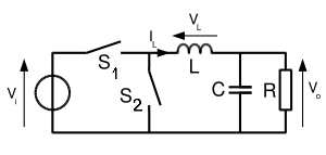
In a standard buck converter, the freewheeling diode turns on, on its own, shortly after the switch turns off, as a result of the rising voltage across the diode. This voltage drop across the diode results in a power loss which is equal to
where:
- VD is the voltage drop across the diode at the load current Io,
- D is the duty cycle, and
- Io is the load current.
By replacing diode D with switch S2, which is advantageously selected for low losses, the converter efficiency can be improved. For example, a MOSFET with very low RDSON might be selected for S2, providing power loss on switch 2 which is
By comparing these equations the reader will note that in both cases, power loss is strongly dependent on the duty cycle, D. It stands to reason that the power loss on the freewheeling diode or lower switch will be proportional to its on-time. Therefore, systems designed for low duty cycle operation will suffer from higher losses in the freewheeling diode or lower switch, and for such systems it is advantageous to consider a synchronous buck converter design.
Without actual numbers the reader will find the usefulness of this substitution to be unclear. Consider a computer power supply, where the input is 5 V, the output is 3.3 V, and the load current is 10A. In this case, the duty cycle will be 66% and the diode would be on for 34% of the time. A typical diode with forward voltage of 0.7 V would suffer a power loss of 2.38 W. A well-selected MOSFET with RDSON of 0.015 Ω, however, would waste only 0.51 W in conduction loss. This translates to improved efficiency and reduced heat loss.
Another advantage of the synchronous converter is that it is bi-directional, which lends itself to applications requiring regenerative brakingRegenerative brakeA regenerative brake is an energy recovery mechanism which slows a vehicle or object down by converting its kinetic energy into another form, which can be either used immediately or stored until needed...
. When power is transferred in the "reverse" direction, it acts much like a boost converterBoost converterA boost converter is a power converter with an output DC voltage greater than its input DC voltage. It is a class of switching-mode power supply containing at least two semiconductor switches and at least one energy storage element...
.
The advantages of the synchronous buck converter do not come without cost. First, the lower switch typically costs more than the freewheeling diode. Second, the complexity of the converter is vastly increased due to the need for a complementary-output switch driver.
Such a driver must prevent both switches from being turned on at the same time, a fault known as "shootthrough." The simplest technique for avoiding shootthrough is a time delay between the turn-off of S1 to the turn-on of S2, and vice versa. However, setting this time delay long enough to ensure that S1 and S2 are never both on will itself result in excess power loss. An improved technique for preventing this condition is known as adaptive "non-overlap" protection, in which the voltage at the switch node (the point where S1, S2 and L are joined) is sensed to determine its state. When the switch node voltage passes a preset threshold, the time delay is started. The driver can thus adjust to many types of switches without the excessive power loss this flexibility would cause with a fixed non-overlap time.
Multiphase buck
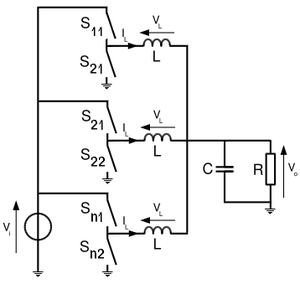 The multiphase buck converter is circuit topology where the basic buck converter circuit are placed in parallel between the input and load. Each of the n "phases" is turned on at equally spaced intervals over the switching period. This circuit is typically used with the synchronous buck topology, described above.
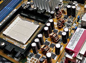
The primary advantage of this type of converter is that it can respond to load changes as quickly as if it switched at n times as fast, without the increase in switching losses that that would cause. Thus, it can respond to rapidly changing loads, such as modern microprocessors.
There is also a significant decrease in switching ripple. Not only is there the decrease due to the increased effective frequency, but any time that n times the duty cycle is an integer, the switching ripple goes to 0; the rate at which the inductor current is increasing in the phases which are switched on exactly matches the rate at which it is decreasing in the phases which are switched off.
Another advantage is that the load current is split among the n phases of the multiphase converter. This load splitting allows the heat losses on each of the switches to be spread across a larger area.
This circuit topology is used in computer power supplies to convert the 12 VDC power supply to a lower voltage (around 1 V), suitable for the CPU. Modern CPU power requirements can exceed 200W, can change very rapidly, and have very tight ripple requirements, less than 10mV. Typical motherboard power supplies use 3 or 4 phases, although control IC manufacturers allow as many as 6 phases
One major challenge inherent in the multiphase converter is ensuring the load current is balanced evenly across the n phases. This current balancing can be performed in a number of ways. Current can be measured "losslessly" by sensing the voltage across the inductor or the lower switch (when it is turned on). This technique is considered lossless because it relies on resistive losses inherent in the buck converter topology. Another technique is to insert a small resistor in the circuit and measure the voltage across it. This approach is more accurate and adjustable, but incurs several costs—space, efficiency and money.
Finally, the current can be measured at the input. Voltage can be measured losslessly, across the upper switch, or using a power resistor, to approximate the current being drawn. This approach is technically more challenging, since switching noise cannot be easily filtered out. However, it is less expensive than emplacing a sense resistor for each phase.
Efficiency factors
Conduction losses that depend on load:- Resistance when the transistor or MOSFET switch is conducting.
- Diode forward voltage drop (usually or for schottky diodeSchottky diodeThe Schottky diode is a semiconductor diode with a low forward voltage drop and a very fast switching action...
) - Inductor winding resistance
- Capacitor equivalent series resistance
Switching losses:- Voltage-Ampere overlap loss
- Frequencyswitch*CV2 loss
- Reverse latence loss
- Losses due driving MOSFET gate and controller consumption.
- Transistor leakage current losses, and controller standby consumption.
Impedance matching
A buck converter can be used to maximize the power transferMaximum power theoremIn electrical engineering, the maximum power transfer theorem states that, to obtain maximum external power from a source with a finite internal resistance, the resistance of the load must be equal to the resistance of the source as viewed from the output terminals...
through the use of impedance matchingImpedance matchingIn electronics, impedance matching is the practice of designing the input impedance of an electrical load to maximize the power transfer and/or minimize reflections from the load....
. An application of this is in a "maximum power point trackerMaximum power point trackerMaximum power point tracking is a technique that grid tie inverters, solar battery chargers and similar devices use to get the maximum possible power from the PV array. Solar cells have a complex relationship between solar irradiation, temperature and total resistance that produces a non-linear...
" commonly used in photovoltaic systems.
By the equation for electric powerElectric powerElectric power is the rate at which electric energy is transferred by an electric circuit. The SI unit of power is the watt.-Circuits:Electric power, like mechanical power, is represented by the letter P in electrical equations...
:

where:- Vo is the output voltage
- Io is the output current
- η is the power efficiency (ranging from 0 to 1)
- Vi is the input voltage
- Ii is the input current
By Ohm's LawOhm's lawOhm's law states that the current through a conductor between two points is directly proportional to the potential difference across the two points...
:


where:- Zo is the output impedanceElectrical impedanceElectrical impedance, or simply impedance, is the measure of the opposition that an electrical circuit presents to the passage of a current when a voltage is applied. In quantitative terms, it is the complex ratio of the voltage to the current in an alternating current circuit...
- Zi is the input impedance
Substituting these expressions for Io and Ii into the power equation yields:
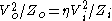
As was previously shown for the continuous mode, (where IL > 0):

where: D is the duty cycle
Substituting this equation for Vo into the previous equation, yields:
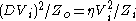
which reduces to:

and finally:

This shows that it is possible to adjust the impedance ratio by adjusting the duty cycle. This is particularly useful in applications where the impedance(s) are dynamically changing.
See also
- Boost converterBoost converterA boost converter is a power converter with an output DC voltage greater than its input DC voltage. It is a class of switching-mode power supply containing at least two semiconductor switches and at least one energy storage element...
- Buck-boost converterBuck-boost converterThe buck–boost converter is a type of DC-to-DC converter that has an output voltage magnitude that is either greater than or less than the input voltage magnitude.Two different topologies are called buck–boost converter....
- Split-PiSplit-PiIn electronics, a split-pi topology is a pattern of component interconnections used in a kind of power converter that can theoretically produce an arbitrary output voltage, either higher or lower than the input voltage. In practice the upper voltage output is limited to the voltage rating of...
(Boost-Buck Converter) - General DC-DC converters and Switched-mode power suppliesSwitched-mode power supplyA switched-mode power supply is an electronic power supply that incorporates a switching regulator in order to be highly efficient in the conversion of electrical power...
External links
- Interactive Power Electronics Seminar (iPES) Many Java applets demonstrating the operation of converters
- Model based control of digital buck converter Description and working VisSimVisSimVisSim is a visual block diagram language for simulation of dynamical systems and model based design of embedded systems. It is developed by Visual Solutions of Westford, Massachusetts....
source code diagram for low cost digital control of DC-DC buck converters - SPICE simulation of the buck converter
- Switch-Mode Power Supply Tutorial - Detailed article on DC-DC converters which gives a more formal and detailed analysis of the Buck including the effects of non-ideal switching (but, note that the diagram of the buck-boost converter fails to account for the inversion of the polarity of the voltage between input and output).

