
Stranski-Krastanov growth
Encyclopedia
Stranski–Krastanov growth (SK growth, also Stransky-Krastanov or Stranski-Krastanow) is one of the three primary modes by which thin film
s grow epitaxially at a crystal surface or interface. Also known as 'layer-plus-island growth', the SK mode follows a two step process: initially, complete films of adsorbates
, up to several monolayer
s thick, grow in a layer-by-layer fashion on a crystal substrate. Beyond a critical layer thickness, which depends on strain
and the chemical potential
of the deposited film, growth continues through the nucleation
and coalescence of adsorbate 'islands'. This growth mechanism was first noted by Ivan Stranski
and Lyubomir Krastanov in 1938. It wasn’t until 1958 however, in a seminal work by Ernst Bauer
published in Zeitschrift für Kristallographie, that the SK, Volmer-Weber, and Frank-van der Merwe mechanisms were systematically classified as the primary thin-film growth processes. Since then, SK growth has been the subject of intense investigation, not only to better understand the complex thermodynamics and kinetics at the core of thin-film formation, but also as a route to fabricating novel nanostructures for application in the microelectronics
industry.
 The growth of epitaxial (homogenous or heterogeneous) thin films on a single crystal surface depends critically on the interaction strength between adatoms
and the surface. While it is possible to grow epilayers from a liquid solution, most epitaxial growth occurs via a vapor phase technique such as molecular beam epitaxy
(MBE). In Volmer–Weber (VW) growth, adatom-adatom interactions are stronger than those of the adatom with the surface, leading to the formation of three-dimensional adatom clusters or islands. Growth of these clusters, along with coarsening
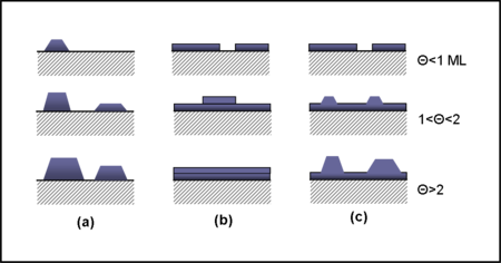
, will cause rough multi-layer films to grow on the substrate surface. Antithetically, during Frank–van der Merwe (FM) growth, adatoms attach preferentially to surface sites resulting in atomically smooth, fully formed layers. This layer-by-layer growth is two dimensional, indicating that complete films form prior to growth of subsequent layers. Stranski–Krastanov growth is an intermediary process characterized by both 2D layer and 3D island growth. Transition from the layer-by-layer to island-based growth occurs at a critical layer thickness which is highly dependent on the chemical and physical properties, such as surface energies and lattice parameters, of the substrate and film. Figure 1 is a schematic representation of the three main growth modes for various surface coverages.
Determining the mechanism by which a thin film grows requires consideration of the chemical potential
s of the first few deposited layers. A model for the layer chemical potential per atom has been proposed by Markov as:

where is the bulk chemical potential of the adsorbate material,
  is the desorption energy of an adsorbate atom from a wetting layer
of the same material, the desorption energy of an adsorbate atom from the substrate,
  is the per atom misfit dislocation energy, and
  the per atom homogeneous strain energy. In general, the values of
  ,
,  ,
,  , and
, and  depend in a complex way on the thickness of the growing layers and lattice misfit between the substrate and adsorbate film. In the limit of small strains,
  , the criterion for a film growth mode is dependent on
  .
.
SK growth can be described by both of these inequalities. While initial film growth follows a FM mechanism, i.e. positive differential μ, non-trivial amounts of strain energy accumulate in the deposited layers. At a critical thickness, this strain induces a sign reversal in the chemical potential, i.e. negative differential μ, leading to a switch in the growth mode. At this point it is energetically favorable to nucleate islands and further growth occurs by a VW type mechanism. A thermodynamic criterion for layer growth similar to the one presented above can be obtained using a force balance of surface tension
s and contact angle
.
Since the formation of wetting layers
occurs in a commensurate fashion at a crystal surface, there is often an associated misfit between the film and the substrate due to the different lattice parameters of each material. Attachment of the thinner film to the thicker substrate induces a misfit strain
at the interface given by . Here
  and
and  are the film and substrate lattice constants, respectively. As the wetting layer thickens, the associated strain energy increases rapidly. In order to relieve the strain, island formation can occur in either a dislocated or coherent fashion. In dislocated islands, strain relief arises by forming interfacial misfit dislocations. The reduction in strain energy accommodated by introducing a dislocation is generally greater than the concomitant cost of increased surface energy associated with creating the clusters. The thickness of the wetting layer at which island nucleation initiates, called the critical thickness
  , is strongly dependent on the lattice mismatch between the film and substrate, with a greater mismatch leading to smaller critical thicknesses. Values of
  can range from sub-monlayer coverage to up to several monolayers thick. Figure 2 illustrates a dislocated island during SK growth after reaching a critical layer height. A pure edge dislocation is shown at the island interface to illustrate the relieved structure of the cluster.
In some cases, most notably the / system, nanoscale dislocation-free islands can be formed during SK growth by introducing undulations into the near surface layers of the substrate. These regions of local curvature serve to elastically deform both the substrate and island, relieving accumulated strain and bringing the wetting layer and island lattice constant closer to its bulk value. This elastic instability at is known as the Grinfeld instability (formerly Asaro-Tiller-Grinfeld; ATG). The resulting islands are coherent and defect-free, garnering them significant interest for use in nanoscale electronic and opto-electronic devices. Such applications are discussed briefly later. A schematic of the resulting epitaxial structure is shown in figure 3 which highlights the induced radius of curvature at the substrate surface and in the island. Finally, it should be noted that strain stabilization indicative of coherent SK growth decreases with decreasing inter-island separation. At large areal island densities (smaller spacing), curvature effects from neighboring clusters will cause dislocation loops to form leading to defected island creation.
 Analytical techniques such as Auger electron spectroscopy
(AES), low-energy electron diffraction (LEED), and reflection high energy electron diffraction
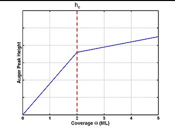
(RHEED), have been extensively used to monitor SK growth. AES data obtained in situ during film growth in a number model systems, such as /(100), Pb
/(110), /W(110), and Ag/(110), show characteristic segmented curves like those presented in figure 4. Height of the film Auger peaks plotted as a function of surface coverage Θ, initially exhibits a straight line, which is indicative of AES data for FM growth. There is a clear break point at a critical adsorbate surface coverage followed by another linear segment at a reduced slope. The paired break point and shallow line slope is characteristic of island nucleation; a similar plot for FM growth would exhibit many such line and break pairs while a plot of the VW mode would be a single line of low slope. In some systems, reorganization of the 2D wetting layer results in decreasing AES peaks with increasing adsorbate coverage. Such situations arise when many adatoms are required to reach a critical nucleus size on the surface and at nucleation the resulting adsorbed layer constitutes a significant fraction of a monolayer. After nucleation, metastable adatoms on the surface are incorporated into the nuclei, causing the Auger signal to fall. This phenomenon is particularly evident for deposits on a molybdenum
substrate.
Evolution of island formation during a SK transitions have also been successfully measured using LEED and RHEED techniques. Diffraction data obtained via various LEED experiments have been effectively used in conjunction with AES to measure the critical layer thickness at the onset of island formation. In addition, RHEED oscillations have proven very sensitive to the layer-to-island transition during SK growth, with the diffraction data providing detailed crystallographic information about the nucleated islands. Following the time dependence of LEED, RHEED, and AES signals, extensive information on surface kinetics and thermodynamics has been gathered for a number of technologically relevant systems.
(TEM), scanning tunneling microscopy (STM), and Atomic force microscopy (AFM) offer the opportunity for direct viewing of deposit/substrate combination events. The extreme magnifications afforded by these techniques, often down to the nanometer length scale, make them particularly applicable for visualizing the strongly 3D islands. UHV-SEM and TEM are routinely used to image island formation during SK growth, enabling a wide range of information to be gathered, ranging from island densities to equilibrium shapes. AFM and STM have become increasingly utilized to correlate island geometry to the surface morphology of the surrounding substrate and wetting layer. These visualization tools are often used to complement quantitative information gathered during wide-beam analyses.
Thin film
A thin film is a layer of material ranging from fractions of a nanometer to several micrometers in thickness. Electronic semiconductor devices and optical coatings are the main applications benefiting from thin film construction....
s grow epitaxially at a crystal surface or interface. Also known as 'layer-plus-island growth', the SK mode follows a two step process: initially, complete films of adsorbates
Adsorption
Adsorption is the adhesion of atoms, ions, biomolecules or molecules of gas, liquid, or dissolved solids to a surface. This process creates a film of the adsorbate on the surface of the adsorbent. It differs from absorption, in which a fluid permeates or is dissolved by a liquid or solid...
, up to several monolayer
Monolayer
- Chemistry :A Langmuir monolayer or insoluble monolayer is a one-molecule thick layer of an insoluble organic material spread onto an aqueous subphase. Traditional compounds used to prepare Langmuir monolayers are amphiphilic materials that possess a hydrophilic headgroup and a hydrophobic tail...
s thick, grow in a layer-by-layer fashion on a crystal substrate. Beyond a critical layer thickness, which depends on strain
Strain
Strain can refer to:* Strain , variants of plants, viruses or bacteria; or an inbred animal used for experimental purposes* Strain , a chemical stress of a molecule...
and the chemical potential
Chemical potential
Chemical potential, symbolized by μ, is a measure first described by the American engineer, chemist and mathematical physicist Josiah Willard Gibbs. It is the potential that a substance has to produce in order to alter a system...
of the deposited film, growth continues through the nucleation
Nucleation
Nucleation is the extremely localized budding of a distinct thermodynamic phase. Some examples of phases that may form by way of nucleation in liquids are gaseous bubbles, crystals or glassy regions. Creation of liquid droplets in saturated vapor is also characterized by nucleation...
and coalescence of adsorbate 'islands'. This growth mechanism was first noted by Ivan Stranski
Ivan Stranski
Ivan Nikolov Stranski was a Bulgarian physical chemist. The founder of the Bulgarian school of physical chemistry, Stranski is considered the father of crystal growth research. Stranski headed the departments of physical chemistry at Sofia University and the Technical University of Berlin, of...
and Lyubomir Krastanov in 1938. It wasn’t until 1958 however, in a seminal work by Ernst Bauer
Ernst G. Bauer
Ernst G. Bauer is a German-American physicist. He is known for his studies in the field of surface science. His most notable contributions are his work on establishing thin film growth and nucleation mechanisms, and his invention of the low energy electron microscope...
published in Zeitschrift für Kristallographie, that the SK, Volmer-Weber, and Frank-van der Merwe mechanisms were systematically classified as the primary thin-film growth processes. Since then, SK growth has been the subject of intense investigation, not only to better understand the complex thermodynamics and kinetics at the core of thin-film formation, but also as a route to fabricating novel nanostructures for application in the microelectronics
Microelectronics
Microelectronics is a subfield of electronics. As the name suggests, microelectronics relates to the study and manufacture of very small electronic components. Usually, but not always, this means micrometre-scale or smaller,. These devices are made from semiconductors...
industry.
Modes of thin-film growth
Adatoms
An adatom is an atom that lies on a crystal surface, and can be thought of as the opposite of a surface vacancy. This term is used in surface chemistry, when describing single atoms lying on surfaces and surface roughness. The word is a contraction of "adsorbed atom"...
and the surface. While it is possible to grow epilayers from a liquid solution, most epitaxial growth occurs via a vapor phase technique such as molecular beam epitaxy
Molecular beam epitaxy
Molecular beam epitaxy is one of several methods of depositing single crystals. It was invented in the late 1960s at Bell Telephone Laboratories by J. R. Arthur and Alfred Y. Cho.-Method:...
(MBE). In Volmer–Weber (VW) growth, adatom-adatom interactions are stronger than those of the adatom with the surface, leading to the formation of three-dimensional adatom clusters or islands. Growth of these clusters, along with coarsening
Ostwald ripening
right|thumb|300px|Basic schematic of the Ostwald ripening process Ostwald ripening is an observed phenomenon in solid solutions or liquid sols which describes the change of an inhomogeneous structure over time...
, will cause rough multi-layer films to grow on the substrate surface. Antithetically, during Frank–van der Merwe (FM) growth, adatoms attach preferentially to surface sites resulting in atomically smooth, fully formed layers. This layer-by-layer growth is two dimensional, indicating that complete films form prior to growth of subsequent layers. Stranski–Krastanov growth is an intermediary process characterized by both 2D layer and 3D island growth. Transition from the layer-by-layer to island-based growth occurs at a critical layer thickness which is highly dependent on the chemical and physical properties, such as surface energies and lattice parameters, of the substrate and film. Figure 1 is a schematic representation of the three main growth modes for various surface coverages.
Determining the mechanism by which a thin film grows requires consideration of the chemical potential
Chemical potential
Chemical potential, symbolized by μ, is a measure first described by the American engineer, chemist and mathematical physicist Josiah Willard Gibbs. It is the potential that a substance has to produce in order to alter a system...
s of the first few deposited layers. A model for the layer chemical potential per atom has been proposed by Markov as:
where
is the bulk chemical potential of the adsorbate material, is the desorption energy of an adsorbate atom from a wetting layerWetting layer
In experimental physics, a wetting layer is an initial layer of atoms that is epitaxially grown on a surface upon which self-assembled quantum dots or thin films are created. The atoms composing a wetting layer can be semimetallic elements/compounds or metallic alloys...
of the same material,
the desorption energy of an adsorbate atom from the substrate, is the per atom misfit dislocation energy, and the per atom homogeneous strain energy. In general, the values of , , , and depend in a complex way on the thickness of the growing layers and lattice misfit between the substrate and adsorbate film. In the limit of small strains, , the criterion for a film growth mode is dependent on .- VW growth:
 (adatom cohesive force is stronger than surface adhesive force)
- FM growth:
 (surface adhesive force is stronger than adatom cohesive force)
SK growth can be described by both of these inequalities. While initial film growth follows a FM mechanism, i.e. positive differential μ, non-trivial amounts of strain energy accumulate in the deposited layers. At a critical thickness, this strain induces a sign reversal in the chemical potential, i.e. negative differential μ, leading to a switch in the growth mode. At this point it is energetically favorable to nucleate islands and further growth occurs by a VW type mechanism. A thermodynamic criterion for layer growth similar to the one presented above can be obtained using a force balance of surface tension
Surface tension
Surface tension is a property of the surface of a liquid that allows it to resist an external force. It is revealed, for example, in floating of some objects on the surface of water, even though they are denser than water, and in the ability of some insects to run on the water surface...
s and contact angle
Contact angle
The contact angle is the angle at which a liquid/vapor interface meets a solid surface. The contact angle is specific for any given system and is determined by the interactions across the three interfaces. Most often the concept is illustrated with a small liquid droplet resting on a flat...
.
Since the formation of wetting layers
Wetting
Wetting is the ability of a liquid to maintain contact with a solid surface, resulting from intermolecular interactions when the two are brought together. The degree of wetting is determined by a force balance between adhesive and cohesive forces.Wetting is important in the bonding or adherence of...
occurs in a commensurate fashion at a crystal surface, there is often an associated misfit between the film and the substrate due to the different lattice parameters of each material. Attachment of the thinner film to the thicker substrate induces a misfit strain
Strain (materials science)
In continuum mechanics, the infinitesimal strain theory, sometimes called small deformation theory, small displacement theory, or small displacement-gradient theory, deals with infinitesimal deformations of a continuum body...
at the interface given by
. Here and are the film and substrate lattice constants, respectively. As the wetting layer thickens, the associated strain energy increases rapidly. In order to relieve the strain, island formation can occur in either a dislocated or coherent fashion. In dislocated islands, strain relief arises by forming interfacial misfit dislocations. The reduction in strain energy accommodated by introducing a dislocation is generally greater than the concomitant cost of increased surface energy associated with creating the clusters. The thickness of the wetting layer at which island nucleation initiates, called the critical thickness , is strongly dependent on the lattice mismatch between the film and substrate, with a greater mismatch leading to smaller critical thicknesses. Values of can range from sub-monlayer coverage to up to several monolayers thick. Figure 2 illustrates a dislocated island during SK growth after reaching a critical layer height. A pure edge dislocation is shown at the island interface to illustrate the relieved structure of the cluster.In some cases, most notably the / system, nanoscale dislocation-free islands can be formed during SK growth by introducing undulations into the near surface layers of the substrate. These regions of local curvature serve to elastically deform both the substrate and island, relieving accumulated strain and bringing the wetting layer and island lattice constant closer to its bulk value. This elastic instability at
is known as the Grinfeld instability (formerly Asaro-Tiller-Grinfeld; ATG). The resulting islands are coherent and defect-free, garnering them significant interest for use in nanoscale electronic and opto-electronic devices. Such applications are discussed briefly later. A schematic of the resulting epitaxial structure is shown in figure 3 which highlights the induced radius of curvature at the substrate surface and in the island. Finally, it should be noted that strain stabilization indicative of coherent SK growth decreases with decreasing inter-island separation. At large areal island densities (smaller spacing), curvature effects from neighboring clusters will cause dislocation loops to form leading to defected island creation.Wide beam techniques
Auger electron spectroscopy
Auger electron spectroscopy is a common analytical technique used specifically in the study of surfaces and, more generally, in the area of materials science...
(AES), low-energy electron diffraction (LEED), and reflection high energy electron diffraction
RHEED
Reflection high-energy electron diffraction is a technique used to characterize the surface of crystalline materials. RHEED systems gather information only from the surface layer of the sample, which distinguishes RHEED from other materials characterization methods that also rely on diffraction of...
(RHEED), have been extensively used to monitor SK growth. AES data obtained in situ during film growth in a number model systems, such as /(100), Pb
Lead
Lead is a main-group element in the carbon group with the symbol Pb and atomic number 82. Lead is a soft, malleable poor metal. It is also counted as one of the heavy metals. Metallic lead has a bluish-white color after being freshly cut, but it soon tarnishes to a dull grayish color when exposed...
/(110), /W(110), and Ag/(110), show characteristic segmented curves like those presented in figure 4. Height of the film Auger peaks plotted as a function of surface coverage Θ, initially exhibits a straight line, which is indicative of AES data for FM growth. There is a clear break point at a critical adsorbate surface coverage followed by another linear segment at a reduced slope. The paired break point and shallow line slope is characteristic of island nucleation; a similar plot for FM growth would exhibit many such line and break pairs while a plot of the VW mode would be a single line of low slope. In some systems, reorganization of the 2D wetting layer results in decreasing AES peaks with increasing adsorbate coverage. Such situations arise when many adatoms are required to reach a critical nucleus size on the surface and at nucleation the resulting adsorbed layer constitutes a significant fraction of a monolayer. After nucleation, metastable adatoms on the surface are incorporated into the nuclei, causing the Auger signal to fall. This phenomenon is particularly evident for deposits on a molybdenum
Molybdenum
Molybdenum , is a Group 6 chemical element with the symbol Mo and atomic number 42. The name is from Neo-Latin Molybdaenum, from Ancient Greek , meaning lead, itself proposed as a loanword from Anatolian Luvian and Lydian languages, since its ores were confused with lead ores...
substrate.
Evolution of island formation during a SK transitions have also been successfully measured using LEED and RHEED techniques. Diffraction data obtained via various LEED experiments have been effectively used in conjunction with AES to measure the critical layer thickness at the onset of island formation. In addition, RHEED oscillations have proven very sensitive to the layer-to-island transition during SK growth, with the diffraction data providing detailed crystallographic information about the nucleated islands. Following the time dependence of LEED, RHEED, and AES signals, extensive information on surface kinetics and thermodynamics has been gathered for a number of technologically relevant systems.
Microscopies
Unlike the techniques presented in the last section in which probe size can be relatively large compared to island size, surface microscopies such scanning electron microscopy (SEM), transmission electron microscopyTransmission electron microscopy
Transmission electron microscopy is a microscopy technique whereby a beam of electrons is transmitted through an ultra thin specimen, interacting with the specimen as it passes through...
(TEM), scanning tunneling microscopy (STM), and Atomic force microscopy (AFM) offer the opportunity for direct viewing of deposit/substrate combination events. The extreme magnifications afforded by these techniques, often down to the nanometer length scale, make them particularly applicable for visualizing the strongly 3D islands. UHV-SEM and TEM are routinely used to image island formation during SK growth, enabling a wide range of information to be gathered, ranging from island densities to equilibrium shapes. AFM and STM have become increasingly utilized to correlate island geometry to the surface morphology of the surrounding substrate and wetting layer. These visualization tools are often used to complement quantitative information gathered during wide-beam analyses.