
Standard cell
Encyclopedia
Application-specific integrated circuit
An application-specific integrated circuit is an integrated circuit customized for a particular use, rather than intended for general-purpose use. For example, a chip designed solely to run a cell phone is an ASIC...
s (ASICs) with mostly digital-logic features. Standard cell methodology is an example of design abstraction, whereby a low-level very-large-scale integration (VLSI) layout
Integrated circuit layout
Integrated circuit layout, also known IC layout, IC mask layout, or mask design, is the representation of an integrated circuit in terms of planar geometric shapes which correspond to the patterns of metal, oxide, or semiconductor layers that make up the components of the integrated circuit.When...
is encapsulated into an abstract logic representation (such as a NAND gate). Cell-based methodology (the general class to which standard cells belong) makes it possible for one designer to focus on the high-level (logical function) aspect of digital design, while another designer focuses on the implementation (physical) aspect. Along with semiconductor manufacturing advances, standard cell methodology has helped designers scale ASICs from comparatively simple single-function ICs (of several thousand gates), to complex multi-million gate system-on-a-chip (SoC) devices.
Construction of a standard cell
A standard cell is a group of transistor and interconnect structures that provides a boolean logic function (e.g., ANDAND gate
The AND gate is a basic digital logic gate that implements logical conjunction - it behaves according to the truth table to the right. A HIGH output results only if both the inputs to the AND gate are HIGH . If neither or only one input to the AND gate is HIGH, a LOW output results...
, OR
OR gate
The OR gate is a digital logic gate that implements logical disjunction - it behaves according to the truth table to the right. A HIGH output results if one or both the inputs to the gate are HIGH . If neither input is HIGH, a LOW output results...
, XOR, XNOR, inverters) or a storage function (flipflop or latch). The simplest cells are direct representations of the elemental NAND, NOR, and XOR boolean function, although cells of much greater complexity are commonly used (such as a 2-bit full-adder, or muxed D-input flipflop.) The cell's boolean logic function is called its logical view: functional behavior is captured in the form of a truth table
Truth table
A truth table is a mathematical table used in logic—specifically in connection with Boolean algebra, boolean functions, and propositional calculus—to compute the functional values of logical expressions on each of their functional arguments, that is, on each combination of values taken by their...
or Boolean algebra equation (for combinational logic), or a state transition table
State transition table
In automata theory and sequential logic, a state transition table is a table showing what state a finite semiautomaton or finite state machine will move to, based on the current state and other inputs...
(for sequential logic
Sequential logic
In digital circuit theory, sequential logic is a type of logic circuit whose output depends not only on the present input but also on the history of the input. This is in contrast to combinational logic, whose output is a function of, and only of, the present input...
).
Usually, the initial design of a standard cell is developed at the transistor level, in the form of a transistor netlist
Netlist
The word netlist can be used in several different contexts, but perhaps the most popular is in the field of electronic design. In this context, a "netlist" describes the connectivity of an electronic design....
or schematic view. The netlist is a nodal description of transistors, of their connections to each other, and of their terminals (ports) to the external environment. A schematic view may be generated with a number of different Computer Aided Design (CAD) or Electronic Design Automation
Electronic design automation
Electronic design automation is a category of software tools for designing electronic systems such as printed circuit boards and integrated circuits...
(EDA) programs that provide a Graphical User Interface
Graphical user interface
In computing, a graphical user interface is a type of user interface that allows users to interact with electronic devices with images rather than text commands. GUIs can be used in computers, hand-held devices such as MP3 players, portable media players or gaming devices, household appliances and...
(GUI) for this netlist generation process. Designers use additional CAD programs such as SPICE
SPICE
SPICE is a general-purpose, open source analog electronic circuit simulator.It is a powerful program that is used in integrated circuit and board-level design to check the integrity of circuit designs and to predict circuit behavior.- Introduction :Unlike board-level designs composed of discrete...
or Spectre
SPECTRE
SPECTRE is a fictional global terrorist organisation featured in the James Bond novels by Ian Fleming, the films based on those novels, and James Bond video games...
to simulate the electronic behavior of the netlist, by declaring input stimulus (voltage or current waveforms) and then calculating the circuit's time domain (analogue) response. The simulations verify whether the netlist implements the desired function and predict other pertinent parameters, such as power consumption or signal propagation delay.
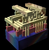
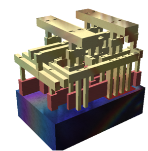
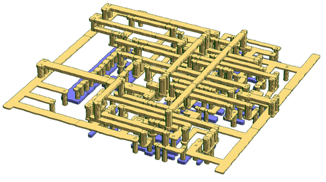
Since the logical and netlist views are only useful for abstract (algebraic) simulation, and not device fabrication, the physical representation of the standard cell must be designed too. Also called the layout view, this is the lowest level of design abstraction in common design practice. From a manufacturing perspective, the standard cell's VLSI layout is the most important view, as it is closest to an actual "manufacturing blueprint" of the standard cell. The layout is organized into base layers, which correspond to the different structures of the transistor devices, and interconnect wiring layers and via layers, which join together the terminals of the transistor formations. The interconnect wiring layers are usually numbered and have specific via layers representing specific connections between each sequential layer. Non-manufacturing layers may be also be present in a layout for purposes of Design Automation, but many layers used explicitly for Place and route
Place and route
Place and route is a stage in the design of printed circuit boards, integrated circuits, and field-programmable gate arrays. As implied by the name, it is composed of two steps, placement and routing. The first step, placement, involves deciding where to place all electronic components, circuitry,...
(PNR) CAD programs are often included in a separate but similar abstract view. The abstract view often contains much less information than the layout and may be recognizable as a Layout Extraction Format (LEF) file or an equivalent.
After a layout is created, additional CAD tools are often used to perform a number of common validations. A Design Rule Check (DRC) is done to verify that the design meets foundry and other layout requirements. A Parasitic EXtractction (PEX)then is performed to generate a PEX-netlist with parasitic properties from the layout. The nodal connections of that netlist are then compared to those of the schematic netlist with a Layout Vs Schematic (LVS) procedure to verify that the connectivity models are equivalent.
The PEX-netlist may then be simulated again (since it contains parasitic properties) to achieve more accurate timing, power, and noise models. These models are often characterized (contained) in a Synopsys
Synopsys
Synopsys, Inc. is one of the largest companies in the Electronic Design Automation industry. Synopsys' first and best-known product is Design Compiler, a logic-synthesis tool. Synopsys offers a wide range of other products used in the design of an application-specific integrated circuit...
Liberty format, but other Verilog
Verilog
In the semiconductor and electronic design industry, Verilog is a hardware description language used to model electronic systems. Verilog HDL, not to be confused with VHDL , is most commonly used in the design, verification, and implementation of digital logic chips at the register-transfer level...
formats may be used as well.
Finally, powerful Place and Route
Place and route
Place and route is a stage in the design of printed circuit boards, integrated circuits, and field-programmable gate arrays. As implied by the name, it is composed of two steps, placement and routing. The first step, placement, involves deciding where to place all electronic components, circuitry,...
(PNR) tools may be used to pull everything together and synthesize (generate) Very Large Scale Integration (VLSI) layouts, in an automated fashion, from higher level design netlists and floor-plans.
Additionally, a number of other CAD tools may be used to validate other aspects of the cell views and models. And other files may be created to support various tools that utilize the standard cells for a plethora of other reasons. All of these files that are created to support the use of all of the standard cell variations are collectively known as a standard cell library.
For a typical Boolean function, there are many different functionally equivalent transistor netlists. Likewise, for a typical netlist, there are many different layouts that fit the netlist's performance parameters. The designer's challenge is to minimize the manufacturing cost of the standard cell's layout (generally by minimizing the circuit's die area), while still meeting the cell's speed and power performance requirements. Consequently, integrated circuit layout
Integrated circuit layout
Integrated circuit layout, also known IC layout, IC mask layout, or mask design, is the representation of an integrated circuit in terms of planar geometric shapes which correspond to the patterns of metal, oxide, or semiconductor layers that make up the components of the integrated circuit.When...
is a highly labor intensive job, despite the existence of design tools to aid this process.
Library
A standard cell library is a collection of low-level logic functions such as AND, OR, INVERT, flip-flops, latches, and buffers. These cells are realized as fixed-height, variable-width full-custom cells. The key aspect with these libraries is that they are of a fixed height, which enables them to be placed in rows, easing the process of automated digital layout. The cells are typically optimized full-custom layouts, which minimize delays and area.A typical standard-cell library contains two main components:
- Library Database - Consists of a number of views often including layout, schematic, symbol, abstract, and other logical or simulation views. From this, various information may be captured in a number of formats including the Cadence LEF format, and the Synopsys Milkyway format, which contain reduced information about the cell layouts, sufficient for automated "Place and Route" tools.
- Timing Abstract - Generally in Liberty format, to provides functional definitions, timing, power, and noise information for each cell.
A standard-cell library may also contain the following additional components:
- A full layout of the cells
- Spice models of the cells
- VerilogVerilogIn the semiconductor and electronic design industry, Verilog is a hardware description language used to model electronic systems. Verilog HDL, not to be confused with VHDL , is most commonly used in the design, verification, and implementation of digital logic chips at the register-transfer level...
models or VHDL Vital models - Parasitic ExtractionParasitic extractionIn electronic design automation, parasitic extraction is calculation of the parasitic effects in both the designed devices and the required wiring interconnects of an electronic circuit: detailed device parameters, parasitic capacitances, parasitic resistances and parasitic inductances, commonly...
models - DRCDesign rule checkingDesign Rule Checking or Check is the area of Electronic Design Automation that determines whether the physical layout of a particular chip layout satisfies a series of recommended parameters called Design Rules...
rule decks
An example is a simple XOR logic gate, which can be formed from OR, INVERT and AND gates.
Application of standard cell
Strictly speaking, a 2-input NAND or NOR function is sufficient to form any arbitrary Boolean function set. But in modern ASIC design, standard-cell methodology is practiced with a sizable library (or libraries) of cells. The library usually contains multiple implementations of the same logic function, differing in area and speed. This variety enhances the efficiency of automated synthesis, place, and route (SPR) tools. Indirectly, it also gives the designer greater freedom to perform implementation trade-offs (area vs. speed vs. power consumption). A complete group of standard-cell descriptions is commonly called a technology library.Commercially available Electronic Design Automation
Electronic design automation
Electronic design automation is a category of software tools for designing electronic systems such as printed circuit boards and integrated circuits...
(EDA) tools use the technology libraries to automate synthesis, placement, and routing of a digital ASIC. The technology library is developed and distributed by the foundry
Foundry
A foundry is a factory that produces metal castings. Metals are cast into shapes by melting them into a liquid, pouring the metal in a mold, and removing the mold material or casting after the metal has solidified as it cools. The most common metals processed are aluminum and cast iron...
operator. The library (along with a design netlist format) is the basis for exchanging design information between different phases of the SPR process.
Synthesis
Using the technology library's cell logical view, the Logic SynthesisLogic synthesis
In electronics, logic synthesis is a process by which an abstract form of desired circuit behavior, typically register transfer level , is turned into a design implementation in terms of logic gates. Common examples of this process include synthesis of HDLs, including VHDL and Verilog...
tool performs the process of mathematically transforming the ASIC's register-transfer level (RTL) description into a technology-dependent netlist. This process is analogous to a software compiler converting a high-level C-program listing into a processor-dependent assembly-language listing.
The netlist is the standard-cell representation of the ASIC design, at the logical view level. It consists of instances of the standard-cell library gates, and port connectivity between gates. Proper synthesis techniques ensure mathematical equivalency between the synthesized netlist and original RTL description. The netlist contains no unmapped RTL statements and declarations.
The high-level synthesis
High-level synthesis
High-level synthesis , sometimes referred to as C synthesis, electronic system level synthesis, algorithmic synthesis, or behavioral synthesis, is an automated design process that interprets an algorithmic description of a desired behavior and creates hardware that implements that behavior. The...
tool performs the process of transforming the C-level models (SystemC, ANSI C/C++) description into a technology-dependent netlist.
Placement
The placementPlacement (EDA)
Placement is an essential step in electronic design automation - the portion of the physical design flow that assigns exact locations for various circuitcomponents within the chip’s core area...
tool starts the physical implementation of the ASIC. With a 2-D floorplan provided by the ASIC designer, the placer tool assigns locations for each gate in the netlist. The resulting placed gates netlist contains the physical location of each of the netlist's standard-cells, but retains an abstract description of how the gates' terminals are wired to each other.
Typically the standard cells have a constant size in at least one dimension that allows them to be lined up in rows on the integrated circuit
Integrated circuit
An integrated circuit or monolithic integrated circuit is an electronic circuit manufactured by the patterned diffusion of trace elements into the surface of a thin substrate of semiconductor material...
. The chip will consist of a huge number of rows (with power and ground running next to each row) with each row filled with the various cells making up the actual design. Placers obey certain rules: Each gate is assigned a unique (exclusive) location on the die map. A given gate is placed once, and may not occupy or overlap the location of any other gate.
Routing
Using the placed-gates netlist and the layout view of the library, the routerRouting (EDA)
In electronic design, wire routing, commonly called simply routing, is a step in the design of printed circuit boards and integrated circuits . It builds on a preceding step, called placement, which determines the location of each active element of an IC or component on a PCB...
adds both signal connect lines and power supply lines. The fully routed physical netlist contains the listing of gates from synthesis, the placement of each gate from placement, and the drawn interconnects from routing.
DRC/LVS
Design rule checking
Design Rule Checking or Check is the area of Electronic Design Automation that determines whether the physical layout of a particular chip layout satisfies a series of recommended parameters called Design Rules...
(DRC) and Layout Versus Schematic
Layout versus schematic
The Layout Versus Schematic is the class of electronic design automation verification software that determines whether a particular integrated circuit layout corresponds to the original schematic or circuit diagram of the design.-Background:...
(LVS) are verification processes. Reliable device fabrication at modern deep-submicrometer (0.13 µm
130 nanometer
The 130 nm process refers to the level of semiconductor process technology that was reached in the 2000–2001 timeframe, by most leading semiconductor companies, like Intel, Texas Instruments, IBM, and TSMC....
and below) requires strict observance of transistor spacing, metal layer thickness, and power density rules. DRC exhaustively compares the physical netlist against a set of "foundry design rules" (from the foundry operator), then flags any observed violations.
The LVS process confirms that the layout has the same structure as the associated schematic; this is typically the final step in the layout process. The LVS tool takes as an input a schematic diagram and the extracted view from a layout. It then generates a netlist from each one and compares them. Nodes, ports, and device sizing are all compared. If they are the same, LVS passes and the designer can continue. LVS tends to consider transistor fingers to be the same as an extra-wide transistor. Thus, 4 transistors in parallel (each 1 μm wide), a 4-finger 1 μm transistor, and a 4 μm transistor are viewed as the same by the LVS tool.
Functionality of .lib files will be taken from SPICE models and added as an attribute to the .lib file.
Other cell-based methodologies
"Standard cell" falls into a more general class of design automation flows called cell-based design. Structured ASICs, FPGAsField-programmable gate array
A field-programmable gate array is an integrated circuit designed to be configured by the customer or designer after manufacturing—hence "field-programmable"...
, and CPLDs are variations on cell-based design. From the designer's standpoint, all share the same input front end: an RTL description of the design. The three techniques, however, differ substantially in the details of the SPR flow and physical implementation.
Complexity measure
For digital standard cell designs, for instance in CMOSCMOS
Complementary metal–oxide–semiconductor is a technology for constructing integrated circuits. CMOS technology is used in microprocessors, microcontrollers, static RAM, and other digital logic circuits...
, a common technology-independent metric for complexity measure is gate equivalents (GE)
Gate equivalent
A gate equivalent stands for a unit of measure which allows to specify manufacturing-technology-independent complexity of digital electronic circuits....
.
See also
- Integrated Circuits
- Circuit DesignCircuit designThe process of circuit design can cover systems ranging from complex electronic systems all the way down to the individual transistors within an integrated circuit...
- SemiconductorSemiconductorA semiconductor is a material with electrical conductivity due to electron flow intermediate in magnitude between that of a conductor and an insulator. This means a conductivity roughly in the range of 103 to 10−8 siemens per centimeter...
- Very-large-scale integrationVery-large-scale integrationVery-large-scale integration is the process of creating integrated circuits by combining thousands of transistors into a single chip. VLSI began in the 1970s when complex semiconductor and communication technologies were being developed. The microprocessor is a VLSI device.The first semiconductor...
(VLSI)
External links
- VLSI Technology— This site contains support material for a book that Graham Petley is writing, The Art of Standard Cell Library Design
- Asic Service - overview of Standard Cell as well as white papers.
- Oklahoma State University— This site contains support material for a complete System on Chip standard cell library that utilizes public-domain and Mentor Graphics/Synopsys/Cadence Design System tools
- Virginia Tech— This is a standard cell library developed by the Virginia Technology VLSI for Telecommunications (VTVT)
- ChipX - Interesting overview of Standard Cell as well as metal layer configurable chip options.