
Design rule checking
Encyclopedia
Design Rule Checking or Check(s) (DRC) is the area of Electronic Design Automation
that determines whether the physical layout of a particular chip layout satisfies a series of recommended parameters called Design Rules. Design rule checking is a major step during Physical verification
signoff on the design, which also involves LVS (Layout versus schematic
) Check, XOR Checks, ERC (Electrical Rule Check) and Antenna Checks. For advanced processes some fabs also insist upon the use of more restricted rules
to improve yield.
 Design Rules are a series of parameters provided by semiconductor manufacturer
s that enable the designer to verify the correctness of a mask set
. Design rules are specific to a particular semiconductor manufacturing process. A design rule set specifies certain geometric and connectivity restrictions to ensure sufficient margins to account for variability in semiconductor manufacturing processes, so as to ensure that most of the parts work correctly.
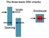
The most basic design rules are shown in the diagram on the right. The first are single layer rules. A width rule specifies the minimum width of any shape in the design. A spacing rule specifies the minimum distance between two adjacent objects. These rules will exist for each layer of semiconductor manufacturing process, with the lowest layers having the smallest rules (typically 100 nm as of 2007) and the highest metal layers having larger rules (perhaps 400 nm as of 2007).
A two layer rule specifies a relationship that must exist between two layers. For example, an enclosure rule might specify that an object of one type, such as a contact or via, must be covered, with some additional margin, by a metal layer. A typical value as of 2007 might be about 10 nm.
There are many other rule types not illustrated here. A minimum area rule is just what the name implies. Antenna rules
are complex rules that check ratios of areas of every layer of a net for configurations that can result in problems when intermediate layers are etched. Many other such rules exist and are explained in detail in the documentation provided by the semiconductor manufacturer.
Academic design rules are often specified in terms of a scalable parameter, λ, so that all geometric tolerances in a design may be defined as integer multiples of λ. This simplifies the migration of existing chip layouts to newer processes. Industrial rules are more highly optimized, and only approximate uniform scaling. Design rule sets have become increasingly more complex with each subsequent generation of semiconductor process.
(DRC) is to achieve a high overall yield and reliability for the design. If design rules are violated the design may not be functional. To meet this goal of improving die yields, DRC has evolved from simple measurement and Boolean checks, to more involved rules that modify existing features, insert new features, and check the entire design for process limitations such as layer density. A completed layout consists not only of the geometric representation of the design, but also data that provides support for the manufacture of the design. While design rule checks do not validate that the design will operate correctly, they are constructed to verify that the structure meets the process constraints for a given design type and process technology.
DRC software usually takes as input a layout in the GDSII
standard format and a list of rules specific to the semiconductor process chosen for fabrication. From these it produces a report of design rule violations that the designer may or may not choose to correct. Carefully "stretching" or waiving certain design rules is often used to increase performance and component density at the expense of yield.
DRC products define rules in a language to describe the operations needed to be performed in DRC. For example, Mentor Graphics uses Standard Verification Rule Format (SVRF) language in their DRC rules files and Magma Design Automation is using TCL
-based language. A set of rules for a particular process is referred to as a run-set, rule deck, or just a deck.
DRC is a very computationally intense task. Usually DRC checks will be run on each sub-section of the ASIC to minimize the number of errors that are detected at the top level. If run on a single CPU, customers may have to wait up to a week to get the result of a Design Rule check for modern designs. Most design companies require DRC to run in less than a day to achieve reasonable cycle times since the DRC will likely be run several times prior to design completion. With today's processing power, full-chip DRC's may run in much shorter times as quick as one hour depending on the chip complexity and size.
Some example of DRC's in IC design include:
All these companies are working on versions that run on many CPUs, to dramatically reduce the elapsed time required.
Estimated annual sales of DRC software are in the $200 to $300 million range. The cost of a single site license of semiconductor EDA software, including DRC components, may exceed $1 million.
Electronic design automation
Electronic design automation is a category of software tools for designing electronic systems such as printed circuit boards and integrated circuits...
that determines whether the physical layout of a particular chip layout satisfies a series of recommended parameters called Design Rules. Design rule checking is a major step during Physical verification
Physical verification
Physical verification is a process whereby an IC layout design is checked via EDA software tools to see if it meets certain criteria. Verification involves DRC , LVS , ERC , XOR , and Antenna Checks.- XOR Check:This check is typically run after a metal spin, where the original and modified database...
signoff on the design, which also involves LVS (Layout versus schematic
Layout versus schematic
The Layout Versus Schematic is the class of electronic design automation verification software that determines whether a particular integrated circuit layout corresponds to the original schematic or circuit diagram of the design.-Background:...
) Check, XOR Checks, ERC (Electrical Rule Check) and Antenna Checks. For advanced processes some fabs also insist upon the use of more restricted rules
Restrictive Design Rules
Design rules are maintained and released by a semiconductor foundry for its customers to follow. Restrictive design rules curtail some of the "freedom" layout designers have traditionally had with regular design rules in less advanced process technologies...
to improve yield.
Design Rules
Semiconductor fabrication
Semiconductor device fabrication is the process used to create the integrated circuits that are present in everyday electrical and electronic devices. It is a multiple-step sequence of photolithographic and chemical processing steps during which electronic circuits are gradually created on a wafer...
s that enable the designer to verify the correctness of a mask set
Mask set
A mask set is a series of electronic data that define geometry for the photolithography steps of semiconductor fabrication. Each of the physical masks generated from this data is called a photomask....
. Design rules are specific to a particular semiconductor manufacturing process. A design rule set specifies certain geometric and connectivity restrictions to ensure sufficient margins to account for variability in semiconductor manufacturing processes, so as to ensure that most of the parts work correctly.
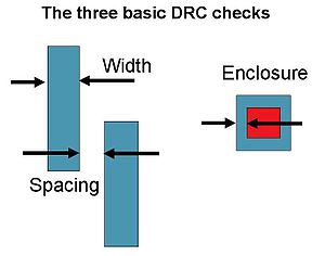
The most basic design rules are shown in the diagram on the right. The first are single layer rules. A width rule specifies the minimum width of any shape in the design. A spacing rule specifies the minimum distance between two adjacent objects. These rules will exist for each layer of semiconductor manufacturing process, with the lowest layers having the smallest rules (typically 100 nm as of 2007) and the highest metal layers having larger rules (perhaps 400 nm as of 2007).
A two layer rule specifies a relationship that must exist between two layers. For example, an enclosure rule might specify that an object of one type, such as a contact or via, must be covered, with some additional margin, by a metal layer. A typical value as of 2007 might be about 10 nm.
There are many other rule types not illustrated here. A minimum area rule is just what the name implies. Antenna rules
Antenna effect
The antenna effect, more formally plasma induced gate oxide damage, is an effect that can potentially cause yield and reliability problems during the manufacture of MOS integrated circuits. Fabs normally supply antenna rules, which are rules that must be obeyed to avoid this problem. A violation...
are complex rules that check ratios of areas of every layer of a net for configurations that can result in problems when intermediate layers are etched. Many other such rules exist and are explained in detail in the documentation provided by the semiconductor manufacturer.
Academic design rules are often specified in terms of a scalable parameter, λ, so that all geometric tolerances in a design may be defined as integer multiples of λ. This simplifies the migration of existing chip layouts to newer processes. Industrial rules are more highly optimized, and only approximate uniform scaling. Design rule sets have become increasingly more complex with each subsequent generation of semiconductor process.
Design Rule Checking Software
The main objective of design rule checking(DRC) is to achieve a high overall yield and reliability for the design. If design rules are violated the design may not be functional. To meet this goal of improving die yields, DRC has evolved from simple measurement and Boolean checks, to more involved rules that modify existing features, insert new features, and check the entire design for process limitations such as layer density. A completed layout consists not only of the geometric representation of the design, but also data that provides support for the manufacture of the design. While design rule checks do not validate that the design will operate correctly, they are constructed to verify that the structure meets the process constraints for a given design type and process technology.
DRC software usually takes as input a layout in the GDSII
GDSII
GDSII stream format, common acronym GDSII, is a database file format which is the de facto industry standard for data exchange of integrated circuit or IC layout artwork. It is a binary file format representing planar geometric shapes, text labels, and other information about the layout in...
standard format and a list of rules specific to the semiconductor process chosen for fabrication. From these it produces a report of design rule violations that the designer may or may not choose to correct. Carefully "stretching" or waiving certain design rules is often used to increase performance and component density at the expense of yield.
DRC products define rules in a language to describe the operations needed to be performed in DRC. For example, Mentor Graphics uses Standard Verification Rule Format (SVRF) language in their DRC rules files and Magma Design Automation is using TCL
TCL
TCL or Tcl may mean:* Biochemistry** TCL * Companies** TCL Corporation, a Chinese electronics company** Twin City Lines, former public transit via streetcar in Minneapolis*Computer languages...
-based language. A set of rules for a particular process is referred to as a run-set, rule deck, or just a deck.
DRC is a very computationally intense task. Usually DRC checks will be run on each sub-section of the ASIC to minimize the number of errors that are detected at the top level. If run on a single CPU, customers may have to wait up to a week to get the result of a Design Rule check for modern designs. Most design companies require DRC to run in less than a day to achieve reasonable cycle times since the DRC will likely be run several times prior to design completion. With today's processing power, full-chip DRC's may run in much shorter times as quick as one hour depending on the chip complexity and size.
Some example of DRC's in IC design include:
- Active to active spacing
- Well to well spacing
- Minimum channel length of the transistor
- Minimum metal width
- Metal to metal spacing
- Metal fill density (for processes using CMP)
- ESD and I/O rules
Commercial DRC Software
Major products in the DRC area of EDA are:- "fiXtress" by BQR
- "ALINT" by ALDEC
- "HiPer Verify" by Tanner EDA
- Calibre by Mentor GraphicsMentor GraphicsMentor Graphics, Inc is a US-based multinational corporation dealing in electronic design automation for electrical engineering and electronics, as of 2004, ranked third in the EDA industry it helped create...
- Guardian DRC by Silvaco Inc.
- Hercules and IC Validator by SynopsysSynopsysSynopsys, Inc. is one of the largest companies in the Electronic Design Automation industry. Synopsys' first and best-known product is Design Compiler, a logic-synthesis tool. Synopsys offers a wide range of other products used in the design of an application-specific integrated circuit...
- Diva, Dracula, Assura and PVS by Cadence Design SystemsCadence Design SystemsCadence Design Systems, Inc is an electronic design automation software and engineering services company, founded in 1988 by the merger of SDA Systems and ECAD, Inc...
- Quartz by Magma Design AutomationMagma Design AutomationMagma Design Automation is a software company in the electronic design automation industry. The company was founded in 1997 and maintains headquarters in San Jose, California, with facilities throughout North America, Europe, Japan, Asia and India....
- Advanced Design SystemAdvanced Design SystemAdvanced Design System is an electronic design automation software system produced by Agilent EEsof EDA , a unit of Agilent Technologies. It provides an integrated design environment to designers of RF electronic products such as mobile phones, pagers, wireless networks, satellite communications,...
Design Rule Checker by Agilent's EEsofEEsofEEsof is an EDA company founded in 1983 by an entrepreneur, Charles J. Abronson, and a former Compact Software employee, Bill Childs.-History:...
EDA division - VERI and HVERI by Zeni EDA
- Some semiconductor companies have their own proprietary DRC software.
All these companies are working on versions that run on many CPUs, to dramatically reduce the elapsed time required.
Estimated annual sales of DRC software are in the $200 to $300 million range. The cost of a single site license of semiconductor EDA software, including DRC components, may exceed $1 million.