

Semiconductor package
Encyclopedia
A semiconductor package is a metal, plastic, glass, or ceramic casing containing one or more semiconductor
electronic components. Individual discrete components are typically etched in silicon wafer before being cut and assembled in a package. The package provides protection against impact and corrosoion, holds the contact pins or leads which are used to connect from external circuits to the device, and dissipates heat produced in the device.
Thousands of standard package types are made,with some made to industry-wide standards and some particular to an individual manufacturer.
s, a package may have hundreds of connections. Very small packages may be supported only by their wire leads. Larger devices, intended for high-power applications, are installed in carefully designed heat sink
s so that they can dissipate hundred or thousands of watts of waste heat.
In addition to providing connections to the semiconductor and handling waste heat, the semiconductor package must protect the "chip" from the environment, particularly the ingress of moisture. Stray particles or corrosion products inside the package may degrade performance of the device or cause failure. A hermetic package allows essentially no gas exchange with the surroundings; such construction requires glass, ceramic or metal enclosures.
and the leads of the package, wire bonds are used, with fine wires connected from the package leads and bonded to conductive pads on the semiconductor die.
At the outside of the package, wire leads may be soldered to a printed circuit board
or used to secure the device to a tag strip. Modern surface mount devices eliminate most of the drilled holes through circuit boards, and have short metal leads or pads on the package that can be secured by wave soldering. Aerospace devices in flat pack
s may use flat metal leads secured to a circuit board by spot welding, though this type of construction is now uncommon.
Early semiconductor devices were often inserted in sockets, like vacuum tube
s. As devices improved, eventually sockets proved unnecessary for reliability, and devices were directly soldered to printed circuit boards. The package must handle the high temperature gradients of soldering without putting stress on the semiconductor die or its leads.
plastic that provides adequate protection of the semiconductor device, and mechanical strength to support the leads and handling of the package. Some devices, intended for high-reliability or aerospace or radiation environments, use ceramic packages, with metal lids that are brazed on after assembly, or a glass frit
seal. All-metal packages are often used with high power (several watts or more) devices, since they conduct heat well and allow for easy assembly to a heat sink. Often the package forms one contact for the semiconductor device. Lead materials must be chosen with a thermal coefficient of expansion to match the package material.
A very few early semiconductors were packed in miniature evacuated glass envelopes, like flashlight bulbs; such expensive packaging was made obsolete when surface passivation and improved manufacturing techniques were available. Glass packages are still commonly used with diodes, and glass seals are used in metal transistor packages.
Package materials for high-density dynamic memory must be selected for low background radiation; a single alpha particle
emitted by package material can cause a single event upset
and transient memory errors.
A modern example of multi-chip integrated circuit packages would be certain models of microprocessor, which may include separate dies for such things as cache memory within the same package.
In a technique called flip chip
, digital integrated circuit dies are inverted and soldered to a module carrier, for assembly into large systems. The technnique was applied by IBM
in their System/360
computers.
device needs a quartz window to allow ultraviolet light to enter and erase the memory. Pressure-sensing integrated circuits require a port on the package that can be connected to a gas or liquid pressure source.
Packages for microwave
frequency devices are arranged to have minimal parasitic inductance and capacitance in their leads. Very-high-impedance devices with ultralow leakage current require packages that do not allow stray current to flow, and may also have guard rings around input terminals. Special isolation amplifier devices include high-voltage insulating barriers between input and output, allowing connection to circuits energized at 1 kV or more.
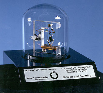
The very first point-contact transistor
s used metal cartridge-style packages with an opening that allowed adjustment of the whisker used to make contact with the germanium
crystal; such devices were common for only a brief time since more reliable, less labor-intensive types were developed.
s, semiconductor packages standards may be defined by national or international industry associations such as JEDEC
, Pro Electron
, or EIAJ, or may be proprietary to a single manufacturer.
Semiconductor
A semiconductor is a material with electrical conductivity due to electron flow intermediate in magnitude between that of a conductor and an insulator. This means a conductivity roughly in the range of 103 to 10−8 siemens per centimeter...
electronic components. Individual discrete components are typically etched in silicon wafer before being cut and assembled in a package. The package provides protection against impact and corrosoion, holds the contact pins or leads which are used to connect from external circuits to the device, and dissipates heat produced in the device.
Thousands of standard package types are made,with some made to industry-wide standards and some particular to an individual manufacturer.
Package functions
A semiconductor package may have as few as two leads or contacts for devices such as diodes, or in the case of advanced microprocessorMicroprocessor
A microprocessor incorporates the functions of a computer's central processing unit on a single integrated circuit, or at most a few integrated circuits. It is a multipurpose, programmable device that accepts digital data as input, processes it according to instructions stored in its memory, and...
s, a package may have hundreds of connections. Very small packages may be supported only by their wire leads. Larger devices, intended for high-power applications, are installed in carefully designed heat sink
Heat sink
A heat sink is a term for a component or assembly that transfers heat generated within a solid material to a fluid medium, such as air or a liquid. Examples of heat sinks are the heat exchangers used in refrigeration and air conditioning systems and the radiator in a car...
s so that they can dissipate hundred or thousands of watts of waste heat.
In addition to providing connections to the semiconductor and handling waste heat, the semiconductor package must protect the "chip" from the environment, particularly the ingress of moisture. Stray particles or corrosion products inside the package may degrade performance of the device or cause failure. A hermetic package allows essentially no gas exchange with the surroundings; such construction requires glass, ceramic or metal enclosures.
Leads
To make connections between an integrated circuitIntegrated circuit
An integrated circuit or monolithic integrated circuit is an electronic circuit manufactured by the patterned diffusion of trace elements into the surface of a thin substrate of semiconductor material...
and the leads of the package, wire bonds are used, with fine wires connected from the package leads and bonded to conductive pads on the semiconductor die.
At the outside of the package, wire leads may be soldered to a printed circuit board
Printed circuit board
A printed circuit board, or PCB, is used to mechanically support and electrically connect electronic components using conductive pathways, tracks or signal traces etched from copper sheets laminated onto a non-conductive substrate. It is also referred to as printed wiring board or etched wiring...
or used to secure the device to a tag strip. Modern surface mount devices eliminate most of the drilled holes through circuit boards, and have short metal leads or pads on the package that can be secured by wave soldering. Aerospace devices in flat pack
Flatpack (electronics)
Flatpack is a US military standardized Printed-circuit-board surface-mount-component package. The military standard MIL-STD-1835C defines: Flat package...
s may use flat metal leads secured to a circuit board by spot welding, though this type of construction is now uncommon.
Early semiconductor devices were often inserted in sockets, like vacuum tube
Vacuum tube
In electronics, a vacuum tube, electron tube , or thermionic valve , reduced to simply "tube" or "valve" in everyday parlance, is a device that relies on the flow of electric current through a vacuum...
s. As devices improved, eventually sockets proved unnecessary for reliability, and devices were directly soldered to printed circuit boards. The package must handle the high temperature gradients of soldering without putting stress on the semiconductor die or its leads.
Package materials
Many devices are molded out of an epoxyEpoxy
Epoxy, also known as polyepoxide, is a thermosetting polymer formed from reaction of an epoxide "resin" with polyamine "hardener". Epoxy has a wide range of applications, including fiber-reinforced plastic materials and general purpose adhesives....
plastic that provides adequate protection of the semiconductor device, and mechanical strength to support the leads and handling of the package. Some devices, intended for high-reliability or aerospace or radiation environments, use ceramic packages, with metal lids that are brazed on after assembly, or a glass frit
Frit
Frit is a ceramic composition that has been fused in a special fusing oven, quenched to form a glass, and granulated. Frits form an important part of the batches used in compounding enamels and ceramic glazes; the purpose of this pre-fusion is to render any soluble and/or toxic components insoluble...
seal. All-metal packages are often used with high power (several watts or more) devices, since they conduct heat well and allow for easy assembly to a heat sink. Often the package forms one contact for the semiconductor device. Lead materials must be chosen with a thermal coefficient of expansion to match the package material.
A very few early semiconductors were packed in miniature evacuated glass envelopes, like flashlight bulbs; such expensive packaging was made obsolete when surface passivation and improved manufacturing techniques were available. Glass packages are still commonly used with diodes, and glass seals are used in metal transistor packages.
Package materials for high-density dynamic memory must be selected for low background radiation; a single alpha particle
Alpha particle
Alpha particles consist of two protons and two neutrons bound together into a particle identical to a helium nucleus, which is classically produced in the process of alpha decay, but may be produced also in other ways and given the same name...
emitted by package material can cause a single event upset
Single event upset
A single event upset is a change of state caused by ions or electro-magnetic radiation striking a sensitive node in a micro-electronic device, such as in a microprocessor, semiconductor memory, or power transistors. The state change is a result of the free charge created by ionization in or close...
and transient memory errors.
Hybrid integrated circuits
Multiple semiconductor dies and discrete components can be assembled on a ceramic substrate and interconnected with wire bonds. The substrate bears leads for connection to an external circuit, and the whole is covered with a welded or frit cover. Such devices are used when requirements exceed the performance (heat dissipation, noise, voltage rating, leakage current, or other properties) available in a single-die integrated circuit, or for mixing analog and digital functions in the same package. Such packages are relatively expensive to manufacture, but provide most of the other benefits of integrated circuits.A modern example of multi-chip integrated circuit packages would be certain models of microprocessor, which may include separate dies for such things as cache memory within the same package.
In a technique called flip chip
Flip chip
Flip chip, also known as Controlled Collapse Chip Connection or its acronym, C4, is a method for interconnecting semiconductor devices, such as IC chips and Microelectromechanical systems , to external circuitry with solder bumps that have been deposited onto the chip pads...
, digital integrated circuit dies are inverted and soldered to a module carrier, for assembly into large systems. The technnique was applied by IBM
IBM
International Business Machines Corporation or IBM is an American multinational technology and consulting corporation headquartered in Armonk, New York, United States. IBM manufactures and sells computer hardware and software, and it offers infrastructure, hosting and consulting services in areas...
in their System/360
System/360
The IBM System/360 was a mainframe computer system family first announced by IBM on April 7, 1964, and sold between 1964 and 1978. It was the first family of computers designed to cover the complete range of applications, from small to large, both commercial and scientific...
computers.
Special packages
Semiconductor packages may include special features. Light-emitting or light-sensing devices must have a transparent window in the package; other devices such as transistors may be disturbed by stray light and require an opaque package. An ultraviolet erasible programmable read-only memoryEPROM
An EPROM , or erasable programmable read only memory, is a type of memory chip that retains its data when its power supply is switched off. In other words, it is non-volatile. It is an array of floating-gate transistors individually programmed by an electronic device that supplies higher voltages...
device needs a quartz window to allow ultraviolet light to enter and erase the memory. Pressure-sensing integrated circuits require a port on the package that can be connected to a gas or liquid pressure source.
Packages for microwave
Microwave
Microwaves, a subset of radio waves, have wavelengths ranging from as long as one meter to as short as one millimeter, or equivalently, with frequencies between 300 MHz and 300 GHz. This broad definition includes both UHF and EHF , and various sources use different boundaries...
frequency devices are arranged to have minimal parasitic inductance and capacitance in their leads. Very-high-impedance devices with ultralow leakage current require packages that do not allow stray current to flow, and may also have guard rings around input terminals. Special isolation amplifier devices include high-voltage insulating barriers between input and output, allowing connection to circuits energized at 1 kV or more.
The very first point-contact transistor
Point-contact transistor
A point-contact transistor was the first type of solid-state electronic transistor ever constructed. It was made by researchers John Bardeen and Walter Houser Brattain at Bell Laboratories in December 1947. They worked in a group led by physicist William Bradford Shockley...
s used metal cartridge-style packages with an opening that allowed adjustment of the whisker used to make contact with the germanium
Germanium
Germanium is a chemical element with the symbol Ge and atomic number 32. It is a lustrous, hard, grayish-white metalloid in the carbon group, chemically similar to its group neighbors tin and silicon. The isolated element is a semiconductor, with an appearance most similar to elemental silicon....
crystal; such devices were common for only a brief time since more reliable, less labor-intensive types were developed.
Standards
Just like vacuum tubeVacuum tube
In electronics, a vacuum tube, electron tube , or thermionic valve , reduced to simply "tube" or "valve" in everyday parlance, is a device that relies on the flow of electric current through a vacuum...
s, semiconductor packages standards may be defined by national or international industry associations such as JEDEC
JEDEC
The JEDEC Solid State Technology Association, formerly known as the Joint Electron Devices Engineering Council , is an independent semiconductor engineering trade organization and standardization body...
, Pro Electron
Pro Electron
Pro Electron is the European type designation and registration system for active components .Pro Electron was set up in 1966 in Brussels, Belgium...
, or EIAJ, or may be proprietary to a single manufacturer.
See also
- Chip carrierChip carrierA chip carrier, also known as a chip container or chip package, is a container for a transistor or an integrated circuit. The carrier usually provides metal leads, or "pins", which are sturdy enough to electrically and mechanically connect the fragile chip to a circuit board. This connection may be...
- DO-204DO-204DO-204 is a family of semiconductor packages defined by JEDEC. This family comprises lead-mounted axial devices with round leads. Several common packages such as DO-41 are archived in DO-204 as variants....
- D2PAKD2PAKThe D2PAK or DDPAK, aka refers to a semiconductor package type intended for surface mounting on circuit boards. They are similar to the earlier TO-220-style packages intended for high power dissipation but lack the extended metal tab and mounting hole.As with all SMT packages, the pins on a D2PAK...
- Gold-aluminium intermetallicGold-aluminium intermetallicA gold-aluminium intermetallic is an intermetallic compound of gold and aluminium that occurs at contacts between the two metals. These intermetallics have different properties than the individual metals which can cause problems in wire bonding in microelectronics...
(purple plague) - Integrated circuit packagingIntegrated circuit packagingIntegrated circuit packaging is the final stage of semiconductor device fabrication per se, followed by IC testing.Packaging in ceramic or plastic prevents physical damage and corrosion and supports the electrical contacts required to assemble the integrated circuit into a system.In the integrated...
- List of electronics package dimensions
- IBM Solid Logic Technology
- Surface-mount technologySurface-mount technologySurface mount technology is a method for constructing electronic circuits in which the components are mounted directly onto the surface of printed circuit boards . An electronic device so made is called a surface mount device...
- Through-hole technologyThrough-hole technologyThrough-hole technology, also spelled "thru-hole", refers to the mounting scheme used for electronic components that involves the use of leads on the components that are inserted into holes drilled in printed circuit boards and soldered to pads on the opposite side either by manual assembly by...
- TO-3
- TO-18TO-18In electronics, TO-18 is a designation for a style of transistor metal case. The case is made of metal and is therefore more expensive than the similarly sized plastic TO-92 package used for other transistors. The name is from JEDEC, signifying Transistor Outline Package, Case Style...
- TO-92
- TO-220