
List of electronics package dimensions
Encyclopedia
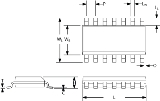
Surface-mount dimension reference
 | C Clearance between IC body and PCB H Total Height T Lead Thickness L Total Carrier Length LW Lead Width LL Lead Length P Pitch WB IC Body Width WL Lead-to-Lead Width |
Through hole pin dimension reference
 | C Clearance between IC body and board H Total Height T Lead Thickness L Total Carrier Length LW Lead Width LL Lead Length P Pitch WB IC Body Width WL Lead-to-Lead Width |
Table of package dimensions
All measurements below are given in mmMillimetre
The millimetre is a unit of length in the metric system, equal to one thousandth of a metre, which is the SI base unit of length....
. To convert mm to mil, divide mm by 0.0254 (ie 2.54 mm / 0.0254 = 100 mill).
C - Clearance between package body and PCB
Printed circuit board
A printed circuit board, or PCB, is used to mechanically support and electrically connect electronic components using conductive pathways, tracks or signal traces etched from copper sheets laminated onto a non-conductive substrate. It is also referred to as printed wiring board or etched wiring...
.
H - Height of package from pin tip to top of package.
T - Thickness of pin.
L - Length of package body only.
LW - Pin width.
LL - Pin length from package to pin tip.
P - Pin pitch (distance between conductors to the PCB).
WB - Width of the package body only.
WL - Length from pin tip to pin tip on the opposite side.
| Image | Family | Pin | Name | Package | WB | WL | H | C | L | P | LL | T | LW |
|---|---|---|---|---|---|---|---|---|---|---|---|---|---|
| CLCC | N | Ceramic Leadless Chip Carrier | 48-CLCC | 14.22 | 14.22 | 2.21 | 14.22 | 1.016 | N/A | 0.508 | |||
 |
PLCC Plastic leaded chip carrier A plastic leaded chip carrier is a chip carrier with a equiangular plastic housing. It is a reduced cost evolution of the ceramic leadless chip carrier .... |
Y | Plastic leaded Chip Carrier | 44-PLCC | |||||||||
 |
DIP Dual in-line package In microelectronics, a dual in-line package is an electronic device package with a rectangular housing and two parallel rows of electrical connecting pins. The package may be through-hole mounted to a printed circuit board or inserted in a socket.A DIP is usually referred to as a DIPn, where n is... |
Y | Dual Inline Package | 8-DIP | 6.2-6.48 | 7.62 | 7.7 | 9.2-9.8 | 2.54 | 3.05-3.6 | 1.14-1.73 | ||
| 32-DIP | 15.24 | 2.54 | |||||||||||
| LFCSP | N | Lead Frame Chip Scale Package | 0.5 | ||||||||||
| MSOP | Y | Mini Small Outline Package | 8-MSOP | 3 | 4.9 | 1.1 | 0.15 | 3 | 0.65 | 0.23 | 0.38 | ||
 |
SOIC Small-Outline Integrated Circuit A small-outline integrated circuit is a surface-mounted integrated circuit package which occupies an area about 30–50% less than an equivalent DIP, with a typical thickness that is 70% less. They are generally available in the same pinouts as their counterpart DIP ICs... SO SOP |
Y | Small Outline Integrated Circuit | 8-SOIC | 3.9 | 5.8-6.2 | 1.72 | 0.10-0.25 | 4.8-5.0 | 1.27 | 1.05 | 0.19-0.25 | 0.39-0.46 |
| 14-SOIC | 3.9 | 5.8-6.2 | 1.72 | 0.10-0.25 | 8.55-8.75 | 1.27 | 1.05 | 0.19-0.25 | 0.39-0.46 | ||||
| 16-SOIC | 3.9 | 5.8-6.2 | 1.72 | 0.10-0.25 | 9.9-10 | 1.27 | 1.05 | 0.19-0.25 | 0.39-0.46 | ||||
| 16-SOIC | 7.5 | 10.00-10.65 | 2.65 | 0.10-0.30 | 10.1-10.5 | 1.27 | 1.4 | 0.23-0.32 | 0.38-0.40 | ||||
 |
SOT | Y | Small Outline Transistor | SOT-23-8 | 1.6 | 2.8 | 1.45 | 2.9 | 0.65 | 0.6 | 0.22-0.38 | ||
| TDFN | ? | Thin Dual Flat No-lead | 8-TDFN | 3 | 3 | 0.7-0.8 | 3 | 0.65 | N/A | 0.19-0.3 | |||
| TSSOP | Y | Thin Shrink Small Outline Package | 8-TSSOP | 4.4 | 6.4 | 1.2 | 0.15 | 3 | 0.65 | 0.09-0.2 | 0.19-0.3 | ||
| µSOP | Y | Micro Small Outline Package | 0.5 | ||||||||||
 |
TQFP | Y | Thin Quad Flat Pack | TQFP-44 | 10.00 | 12.00 | 0.35-0.50 | 0.80 | 1.00 | 0.09-0.20 | 0.30-0.45 | ||
 |
LQFP | Y | Low-profile Quad Flat Package | ||||||||||
| TQFN | N | Thin Quad Flat No-lead |