
Polycrystalline silicon photovoltaics
Encyclopedia
Polycrystalline silicon photovoltaics are a type of solar cell
. Silicon
solar cells are manufactured with a microstructure tailored to the application depending on economic and performance requirements.
, and polycrystalline.
 Presently, polysilicon is commonly used for the conducting gate materials in semiconductor devices such as MOSFET
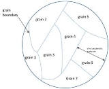
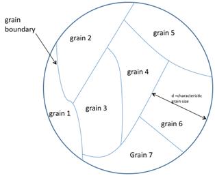
s; however, it has potential for large-scale photovoltaic devices. The abundance, stability, and low toxicity of silicon, combined with the low cost of polysilicon relative to single crystals makes this variety of material attractive for photovoltaic production. Grain size has been shown to have an effect on the efficiency of polycrystalline solar cells. Solar cell efficiency increases with grain size. This effect is due to reduced recombination in the solar cell. Recombination, which is a limiting factor for current in a solar cell, occurs more prevalently at grain boundaries, see figure 1.
The resistivity, mobility, and free-carrier concentration in monocrystalline silicon vary with doping concentration of the single crystal silicon. Whereas the doping of polycrystalline silicon does have an effect on the resistivity, mobility, and free-carrier concentration, these properties strongly depend on the polycrystalline grain size, which is a physical parameter that the material scientist can manipulate. Through the methods of crystallization to form polycrystalline silicon, an engineer can control the size of the polycrystalline grains which will vary the physical properties of the material.
A primary concern in the photovoltaics industry is cell efficiency. However, sufficient cost savings from cell manufacturing can be suitable to offset reduced efficiency in the field, such as the use of larger solar cell arrays compared with more compact/higher efficiency designs. Designs such as CSG are attractive because of a low cost of production even with reduced efficiency. Higher efficiency devices yield modules that occupy less space and are more compact, however the 5-10 % efficiency of typical CSG devices still makes them attractive for installation in large central-service stations, such as a power station. The issue of efficiency versus cost is a value decision of whether one requires an “energy dense” solar cell or sufficient area is available for the installation of less expensive alternatives. For instance, a solar cell used for power generation in a remote location might require a more highly efficient solar cell than one used for low-power applications, such as solar accent lighting or pocket calculators, or near established power grids.
While chalcogen
ide-based Cadmium
-Tellurium (CdTe) and Copper
-Indium
-Selenium
(CIS) polycrystalline thin films cells have been developed in the lab with great success, there is still industry interest in silicon-based thin film cells. Silicon-based devices exhibit fewer problems than their CdTe and CIS counterparts such as toxicity and humidity issues with CdTe cells and low manufacturing yields of CIS due to material complexity. Additionally, due to political resistance to the use non-“green” materials in solar energy production, there is no stigma in the use of standard silicon. Three major silicon-based module designs dominate: amorphous silicon cells, amorphous / microcrystalline tandem cells, and thin-film polycrystalline silicon on glass.
Amorphous / microcrystalline silicon consists of a mixed phase of small crystalline regions surrounded by amorphous material. This material typically behaves more like crystalline silicon than the amorphous variety. A 3-month field study has shown that hybrid amorphous / microcrystalline cells degrade roughly to the same degree as triple-junction amorphous cells while maintaining higher conversion efficiencies (7.0% versus 5.0% as measured at the conclusion of the study). This result suggests hybrid designs of this type may supplant traditional amorphous-based modules.
A new attempt to fuse the advantages of bulk silicon with those of thin-film devices is thin film polycrystalline silicon on glass. These modules are produced by depositing an antireflection coating and doped silicon onto textured glass substrates using plasma-enhanced chemical vapor deposition (PECVD). The texture in the glass enhances the efficiency of the cell by approximately 3% by reducing the amount of incident light reflecting from the solar cell and trapping light inside the solar cell. The silicon film is crystallized by an annealing step, temperatures of 400-600 Celsius, resulting in polycrystalline silicon.
These new devices show energy conversion efficiencies of 8% and high manufacturing yields of >90%. Crystalline silicon on glass (CSG), where the polycrystalline silicon is 1-2 micrometres, is noted for its stability and durability; the use of thin film techniques also contributes to a cost savings over bulk photovoltaics. These modules do not require the presence of a transparent conducting oxide layer. This simplifies the production process twofold; not only can this step be skipped, but the absence of this layer makes the process of constructing a contact scheme much simpler. Both of these simplifications further reduce the cost of production. Despite the numerous advantages over alternative design, production cost estimations on a per unit area basis show that these devices are comparable in cost to single-junction amorphous thin film cells.
In both of these methods, amorphous silicon (a-Si or a-Si:H) is grown using traditional techniques such as plasma-enhanced chemical vapor deposition (PECVD). The crystallization methods diverge during post-deposition processing.
In aluminum-induced crystallization , a thin layer of aluminum (50 nm or less) is deposited by physical vapor deposition onto the surface of the amorphous silicon. This stack of material is then annealed at a relatively low temperature between 140°C and 200°C in a vacuum. The aluminum that diffuses into the amorphous silicon is believed to weaken the hydrogen bonds present, allowing crystal nucleation and growth. Experiments have shown that polycrystalline silicon with grains on the order of 0.2 – 0.3 μm can be produced at temperatures as low as 150°C. The volume fraction of the film that is crystallized is dependent on the length of the annealing process.
Aluminum-induced crystallization produces polycrystalline silicon with suitable crystallographic and electronic properties that make it a candidate for producing polycrystalline thin films for photovoltaics. AIC can be used to generate crystalline silicon nanowires and other nano-scale structures.
Another method of achieving the same result is the use of a laser to heat the silicon locally without heating the underlying substrate beyond some upper temperature limit. An excimer laser or, alternatively, green lasers such as a frequency-doubled Nd:YAG laser is used to heat the amorphous silicon, supplying energy necessary to nucleate grain growth. The laser fluence must be carefully controlled in order to induce crystallization without causing widespread melting. Crystallization of the film occurs as a very small portion of the silicon film is melted and allowed to cool. Ideally, the laser should melt the silicon film through its entire thickness, but not damage the substrate. Toward this end, a layer of silicon dioxide is sometimes added to act as a thermal barrier. This allows the use of substrates that cannot be exposed to the high temperatures of standard annealing, polymers for instance. Polymer-backed solar cells are of interest for seamlessly integrated power production schemes that involve placing photovoltaics on everyday surfaces.
A third method for crystallizing amorphous silicon is the use of thermal plasma jet. This strategy is an attempt to alleviate some of the problems associated with laser processing – namely the small region of crystallization and the high cost of the process on a production scale. The plasma torch is a simple piece of equipment that is used to thermally anneal the amorphous silicon. Compared to the laser method, this technique is simpler and more cost effective.
Plasma torch annealing is attractive because the process parameters and equipment dimension can be changed easily to yield varying levels of performance. A high level of crystallization (~90%) can be obtained with this method. Disadvantages include difficulty achieving uniformity in the crystallization of the film. While this method is applied frequently to silicon on a glass substrate, processing temperatures may be too high for polymers.
Solar cell
A solar cell is a solid state electrical device that converts the energy of light directly into electricity by the photovoltaic effect....
. Silicon
Silicon
Silicon is a chemical element with the symbol Si and atomic number 14. A tetravalent metalloid, it is less reactive than its chemical analog carbon, the nonmetal directly above it in the periodic table, but more reactive than germanium, the metalloid directly below it in the table...
solar cells are manufactured with a microstructure tailored to the application depending on economic and performance requirements.
Forms of silicon
Silicon for photovoltaic applications is typically divided into three categories—monocrystalline, amorphousAmorphous silicon
Amorphous silicon is the non-crystalline allotropic form of silicon. It can be deposited in thin films at low temperatures onto a variety of substrates, offering some unique capabilities for a variety of electronics.-Description:...
, and polycrystalline.
Monocrystalline
Monocrystalline silicon is a form in which the crystal structure is homogenous throughout the material; the orientation, lattice parameter, and electronic properties are constant throughout the material. Dopant atoms such as phosphorus and boron are often incorporated into the film to make the silicon n-type or p-type respectively. Monocrystalline silicon is fabricated in the form of silicon wafers, usually by the Czochralski Growth method, and can be quite expensive depending on the radial size of the desired single crystal wafer (around $200 for a 300 mm Si wafer). This monocrystalline material, while useful, is one of the chief expenses associated with producing photovoltaics where approximately 40% of the final price of the product is attributable to the cost of the starting silicon wafer used in cell fabrication.Amorphous
Amorphous silicon has no long-range periodic order. The application of amorphous silicon to photovoltaics as a standalone material is somewhat limited by its inferior electronic properties. When paired with microcrystalline silicon in tandem and triple-junction solar cells, however, higher efficiency can be attained than with single-junction solar cells. This tandem assembly of solar cells allows one to obtain a thin-film material with a bandgap of around 1.12 eV (the same as single-crystal silicon) compared to the bandgap of amorphous silicon of 1.7-1.8 eV bandgap[4]. Tandem solar cells are then attractive since they can be fabricated with a bandgap similar to single-crystal silicon but with the ease of amorphous silicon.Polycrystalline
Polycrystalline silicon is composed of many smaller silicon grains of varied crystallographic orientation. This material can be synthesized easily by allowing liquid silicon to cool using a seed crystal of the desired crystal structure. Additionally, other methods for crystallizing amorphous silicon to form polysilicon exist such as high temperature chemical vapor deposition (CVD).Potential for use of polycrystalline silicon
MOSFET
The metal–oxide–semiconductor field-effect transistor is a transistor used for amplifying or switching electronic signals. The basic principle of this kind of transistor was first patented by Julius Edgar Lilienfeld in 1925...
s; however, it has potential for large-scale photovoltaic devices. The abundance, stability, and low toxicity of silicon, combined with the low cost of polysilicon relative to single crystals makes this variety of material attractive for photovoltaic production. Grain size has been shown to have an effect on the efficiency of polycrystalline solar cells. Solar cell efficiency increases with grain size. This effect is due to reduced recombination in the solar cell. Recombination, which is a limiting factor for current in a solar cell, occurs more prevalently at grain boundaries, see figure 1.
The resistivity, mobility, and free-carrier concentration in monocrystalline silicon vary with doping concentration of the single crystal silicon. Whereas the doping of polycrystalline silicon does have an effect on the resistivity, mobility, and free-carrier concentration, these properties strongly depend on the polycrystalline grain size, which is a physical parameter that the material scientist can manipulate. Through the methods of crystallization to form polycrystalline silicon, an engineer can control the size of the polycrystalline grains which will vary the physical properties of the material.
Novel ideas for polycrystalline silicon
The use of polycrystalline silicon in the production of solar cells requires less material and therefore provides for higher profits and increased manufacturing throughput. Polycrystalline silicon does not need to be deposited on a silicon wafer to form a solar cell, rather it can be deposited on other-cheaper materials, thus reducing the cost. Not requiring a silicon wafer alleviates the silicon shortages occasionally faced by the microelectronics industry. An example of not using a silicon wafer is crystalline silicon on glass (CSG) materialsA primary concern in the photovoltaics industry is cell efficiency. However, sufficient cost savings from cell manufacturing can be suitable to offset reduced efficiency in the field, such as the use of larger solar cell arrays compared with more compact/higher efficiency designs. Designs such as CSG are attractive because of a low cost of production even with reduced efficiency. Higher efficiency devices yield modules that occupy less space and are more compact, however the 5-10 % efficiency of typical CSG devices still makes them attractive for installation in large central-service stations, such as a power station. The issue of efficiency versus cost is a value decision of whether one requires an “energy dense” solar cell or sufficient area is available for the installation of less expensive alternatives. For instance, a solar cell used for power generation in a remote location might require a more highly efficient solar cell than one used for low-power applications, such as solar accent lighting or pocket calculators, or near established power grids.
Thin film solar cells
Thin film silicon photovoltaics are typically produced by chemical vapor deposition processes yielding an amorphous, polycrystalline, or nanocrystalline film. Conventionally, amorphous silicon thin films are most common. Silicon is usually deposited on glass, plastic, or metallic substrates coated with a transparent conducting oxide material.While chalcogen
Chalcogen
The chalcogens are the chemical elements in group 16 of the periodic table. This group is also known as the oxygen family...
ide-based Cadmium
Cadmium
Cadmium is a chemical element with the symbol Cd and atomic number 48. This soft, bluish-white metal is chemically similar to the two other stable metals in group 12, zinc and mercury. Similar to zinc, it prefers oxidation state +2 in most of its compounds and similar to mercury it shows a low...
-Tellurium (CdTe) and Copper
Copper
Copper is a chemical element with the symbol Cu and atomic number 29. It is a ductile metal with very high thermal and electrical conductivity. Pure copper is soft and malleable; an exposed surface has a reddish-orange tarnish...
-Indium
Indium
Indium is a chemical element with the symbol In and atomic number 49. This rare, very soft, malleable and easily fusible post-transition metal is chemically similar to gallium and thallium, and shows the intermediate properties between these two...
-Selenium
Selenium
Selenium is a chemical element with atomic number 34, chemical symbol Se, and an atomic mass of 78.96. It is a nonmetal, whose properties are intermediate between those of adjacent chalcogen elements sulfur and tellurium...
(CIS) polycrystalline thin films cells have been developed in the lab with great success, there is still industry interest in silicon-based thin film cells. Silicon-based devices exhibit fewer problems than their CdTe and CIS counterparts such as toxicity and humidity issues with CdTe cells and low manufacturing yields of CIS due to material complexity. Additionally, due to political resistance to the use non-“green” materials in solar energy production, there is no stigma in the use of standard silicon. Three major silicon-based module designs dominate: amorphous silicon cells, amorphous / microcrystalline tandem cells, and thin-film polycrystalline silicon on glass.
Amorphous / microcrystalline silicon consists of a mixed phase of small crystalline regions surrounded by amorphous material. This material typically behaves more like crystalline silicon than the amorphous variety. A 3-month field study has shown that hybrid amorphous / microcrystalline cells degrade roughly to the same degree as triple-junction amorphous cells while maintaining higher conversion efficiencies (7.0% versus 5.0% as measured at the conclusion of the study). This result suggests hybrid designs of this type may supplant traditional amorphous-based modules.
A new attempt to fuse the advantages of bulk silicon with those of thin-film devices is thin film polycrystalline silicon on glass. These modules are produced by depositing an antireflection coating and doped silicon onto textured glass substrates using plasma-enhanced chemical vapor deposition (PECVD). The texture in the glass enhances the efficiency of the cell by approximately 3% by reducing the amount of incident light reflecting from the solar cell and trapping light inside the solar cell. The silicon film is crystallized by an annealing step, temperatures of 400-600 Celsius, resulting in polycrystalline silicon.
These new devices show energy conversion efficiencies of 8% and high manufacturing yields of >90%. Crystalline silicon on glass (CSG), where the polycrystalline silicon is 1-2 micrometres, is noted for its stability and durability; the use of thin film techniques also contributes to a cost savings over bulk photovoltaics. These modules do not require the presence of a transparent conducting oxide layer. This simplifies the production process twofold; not only can this step be skipped, but the absence of this layer makes the process of constructing a contact scheme much simpler. Both of these simplifications further reduce the cost of production. Despite the numerous advantages over alternative design, production cost estimations on a per unit area basis show that these devices are comparable in cost to single-junction amorphous thin film cells.
Low temperature induced crystallization of amorphous silicon
Amorphous silicon can be transformed to crystalline silicon using well-understood and widely implemented high-temperature annealing processes. This typical method is the typical method used in industry but requires high-temperature compatible materials, such as special high temperature glass that is expensive to produce. However, there are many applications for which this is an inherently unattractive production method. Flexible solar cells have been a topic of interest for less conspicuous-integrated power generation than solar power farms. These modules may be placed in areas where traditional cells would not be feasible, such as wrapped around a telephone pole or cell phone tower. In this application a photovoltaic material may be applied to a flexible substrate, often a polymer. Such substrates cannot survive the high temperatures experienced during traditional annealing. Instead, novel methods of crystallizing the silicon without disturbing the underlying substrate have been studied extensively. Aluminum-induced crystallization (AIC) and local laser crystallization are common in the literature, however not extensively used in industry.In both of these methods, amorphous silicon (a-Si or a-Si:H) is grown using traditional techniques such as plasma-enhanced chemical vapor deposition (PECVD). The crystallization methods diverge during post-deposition processing.
In aluminum-induced crystallization , a thin layer of aluminum (50 nm or less) is deposited by physical vapor deposition onto the surface of the amorphous silicon. This stack of material is then annealed at a relatively low temperature between 140°C and 200°C in a vacuum. The aluminum that diffuses into the amorphous silicon is believed to weaken the hydrogen bonds present, allowing crystal nucleation and growth. Experiments have shown that polycrystalline silicon with grains on the order of 0.2 – 0.3 μm can be produced at temperatures as low as 150°C. The volume fraction of the film that is crystallized is dependent on the length of the annealing process.
Aluminum-induced crystallization produces polycrystalline silicon with suitable crystallographic and electronic properties that make it a candidate for producing polycrystalline thin films for photovoltaics. AIC can be used to generate crystalline silicon nanowires and other nano-scale structures.
Another method of achieving the same result is the use of a laser to heat the silicon locally without heating the underlying substrate beyond some upper temperature limit. An excimer laser or, alternatively, green lasers such as a frequency-doubled Nd:YAG laser is used to heat the amorphous silicon, supplying energy necessary to nucleate grain growth. The laser fluence must be carefully controlled in order to induce crystallization without causing widespread melting. Crystallization of the film occurs as a very small portion of the silicon film is melted and allowed to cool. Ideally, the laser should melt the silicon film through its entire thickness, but not damage the substrate. Toward this end, a layer of silicon dioxide is sometimes added to act as a thermal barrier. This allows the use of substrates that cannot be exposed to the high temperatures of standard annealing, polymers for instance. Polymer-backed solar cells are of interest for seamlessly integrated power production schemes that involve placing photovoltaics on everyday surfaces.
A third method for crystallizing amorphous silicon is the use of thermal plasma jet. This strategy is an attempt to alleviate some of the problems associated with laser processing – namely the small region of crystallization and the high cost of the process on a production scale. The plasma torch is a simple piece of equipment that is used to thermally anneal the amorphous silicon. Compared to the laser method, this technique is simpler and more cost effective.
Plasma torch annealing is attractive because the process parameters and equipment dimension can be changed easily to yield varying levels of performance. A high level of crystallization (~90%) can be obtained with this method. Disadvantages include difficulty achieving uniformity in the crystallization of the film. While this method is applied frequently to silicon on a glass substrate, processing temperatures may be too high for polymers.
See also
- List of types of solar cells
- Polymer solar cellPolymer solar cellPolymer solar cells are a type of flexible solar cell. They can come in many forms including: organic solar cell , or organic chemistry photovoltaic cell that produce electricity from sunlight using polymers. There are also other types of more stable thin-film semiconductors that can be deposited...