

Electron beam induced deposition
Encyclopedia
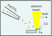
Electron beam-induced deposition (EBID) is a process of decomposing gaseous molecules by electron beam leading to deposition of non-volatile fragments onto a nearby substrate. The electron beam is usually provided by a scanning electron microscope
that results in high spatial accuracy (below one nanometer) and possibility to produce free-standing, three-dimensional structures.
 Focused electron beam of scanning electron microscope
(SEM) or scanning transmission electron microscope (STEM) is commonly used. Focused ion beam
can be applied instead, but then the process is called ion beam-induced deposition (IBID). The precursor material is gas, liquid or solid. Liquid or solids are gasified prior to deposition, usually through vaporization or sublimation, and introduced, at accurately controlled rate, into the high-vacuum chamber of electron microscope. Alternatively, solid precursor is sublimated by the electron beam itself.
When deposition occurs at high temperature or involves corrosive gases, specially designed deposition chamber is used; it is isolated from the microscope, and the beam is introduced into it through a micrometre-sized orifice. Small orifice size maintains differential pressure in the microscope (vacuum) and deposition chamber (no vacuum). Such deposition mode has been used for EBID of diamond.
The electron beam is scanned over desired shape resulting in deposition of material. The scanning is usually computer controlled. The deposition rate depends on the partial pressure and is of the order 10 nm/s.
The most popular precursors for deposition of elemental solids are metal carbonyl
s of Me(CO)x structure or metallocenes. They are easily available, but produce carbon contamination. Metal-halogen complexes (WF6
, etc.) result in cleaner deposition, but they are toxic and corrosive. Compound materials are deposited from specially crafted, exotic gases, e.g. D2GaN3 for GaN.
, usually 30 keV Ga+, is used instead of the electron beam. In both techniques, it is not the primary beam, but secondary electrons which cause the deposition. IBID has the following disadvantages as compared to EBID:
The advantages of IBID are:
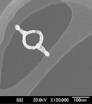 Nanostructures of virtually any 3-dimensional shape can be deposited using computer-controlled scanning of electron beam. Only the starting point has to be attached to the substrate, the rest of the structure can be free standing. The achieved shapes and devices are remarkable:
Scanning electron microscope
A scanning electron microscope is a type of electron microscope that images a sample by scanning it with a high-energy beam of electrons in a raster scan pattern...
that results in high spatial accuracy (below one nanometer) and possibility to produce free-standing, three-dimensional structures.
Process
Scanning electron microscope
A scanning electron microscope is a type of electron microscope that images a sample by scanning it with a high-energy beam of electrons in a raster scan pattern...
(SEM) or scanning transmission electron microscope (STEM) is commonly used. Focused ion beam
Focused ion beam
Focused ion beam, also known as FIB, is a technique used particularly in the semiconductor industry, materials science and increasingly in the biological field for site-specific analysis, deposition, and ablation of materials. An FIB setup is a scientific instrument that resembles a scanning...
can be applied instead, but then the process is called ion beam-induced deposition (IBID). The precursor material is gas, liquid or solid. Liquid or solids are gasified prior to deposition, usually through vaporization or sublimation, and introduced, at accurately controlled rate, into the high-vacuum chamber of electron microscope. Alternatively, solid precursor is sublimated by the electron beam itself.
When deposition occurs at high temperature or involves corrosive gases, specially designed deposition chamber is used; it is isolated from the microscope, and the beam is introduced into it through a micrometre-sized orifice. Small orifice size maintains differential pressure in the microscope (vacuum) and deposition chamber (no vacuum). Such deposition mode has been used for EBID of diamond.
The electron beam is scanned over desired shape resulting in deposition of material. The scanning is usually computer controlled. The deposition rate depends on the partial pressure and is of the order 10 nm/s.
Deposition mechanism
SEM or STEM electrons have energy too high (typically between 10 and 300 keV) to efficiently break molecular bonds. Therefore decomposition occurs via a two-step process: any materials (substrate, holders or the material that has already been deposited) near the deposition spot absorb primary electrons and re-emit secondary electrons having a wide spectrum of energies (of the order 1 keV) and angles. Secondary electrons decompose the precursor molecules.Spatial resolution
Primary STEM electrons can be focused into spots as small as ~0.045 nm. However, the smallest structures deposited so far by EBID are dots of ~0.7 nm diameter. The reason for reduced resolution is wide angular range of secondary electrons, and there is no straightforward way to overcome this problem.Materials and precursors
The range of materials deposited by EBID currently (sept. 2008) includes Al, Au, amorphous carbon, diamond, Co, Cr, Cu, Fe, GaAs, GaN, Ge, Mo, Nb, Ni, Os, Pd, Pt, Rh, Ru, Re, Si, Si3N4, SiOx, TiOx, W, and is being expanded. The limiting factor is availability of appropriate precursors, gaseous or having low sublimation temperature.The most popular precursors for deposition of elemental solids are metal carbonyl
Metal carbonyl
Metal carbonyls are coordination complexes of transition metals with carbon monoxide ligands. These complexes may be homoleptic, that is containing only CO ligands, such as nickel carbonyl , but more commonly metal carbonyls contain a mix of ligands, such as Re3Cl...
s of Me(CO)x structure or metallocenes. They are easily available, but produce carbon contamination. Metal-halogen complexes (WF6
Tungsten(VI) fluoride
Tungsten fluoride, also known as tungsten hexafluoride, is the inorganic compound of tungsten and fluorine with the formula WF6. This corrosive, colorless compound is a gas under standard conditions. With a density of about 13 g/L , WF6 is one of the heaviest known gases under standard conditions...
, etc.) result in cleaner deposition, but they are toxic and corrosive. Compound materials are deposited from specially crafted, exotic gases, e.g. D2GaN3 for GaN.
Advantages
- Deposition occurs in high-vacuum chamber of electron microscope and therefore is rather clean.
- Size of the produced structures and accuracy of deposition are unprecedented.
- The deposited material can be characterized using the electron microscopy techniques (TEMTransmission electron microscopyTransmission electron microscopy is a microscopy technique whereby a beam of electrons is transmitted through an ultra thin specimen, interacting with the specimen as it passes through...
, EELS, EDSEnergy-dispersive X-ray spectroscopyEnergy-dispersive X-ray spectroscopy is an analytical technique used for the elemental analysis or chemical characterization of a sample. It relies on the investigation of an interaction of a some source of X-ray excitation and a sample...
, electron diffractionElectron diffractionElectron diffraction refers to the wave nature of electrons. However, from a technical or practical point of view, it may be regarded as a technique used to study matter by firing electrons at a sample and observing the resulting interference pattern...
) during or right after deposition. In situ electrical and optical characterization is also possible.
Disadvantages
- Complexity of the setup and process limits mass production
- presence of impurities in deposit, from the gaseous phase
Ion beam-induced deposition
Ion beam-induced deposition (IBID) is very similar to EBID with the major difference that focused ion beamFocused ion beam
Focused ion beam, also known as FIB, is a technique used particularly in the semiconductor industry, materials science and increasingly in the biological field for site-specific analysis, deposition, and ablation of materials. An FIB setup is a scientific instrument that resembles a scanning...
, usually 30 keV Ga+, is used instead of the electron beam. In both techniques, it is not the primary beam, but secondary electrons which cause the deposition. IBID has the following disadvantages as compared to EBID:
- Angular spread of secondary electrons is larger in IBID thus resulting in lower spatial resolution.
- Ga+ ions introduce additional contamination and radiation damage to the deposited structure, which is important for electronic applications.
- Deposition occurs in a focused ion beamFocused ion beamFocused ion beam, also known as FIB, is a technique used particularly in the semiconductor industry, materials science and increasingly in the biological field for site-specific analysis, deposition, and ablation of materials. An FIB setup is a scientific instrument that resembles a scanning...
(FIB) setup, which strongly limits characterization of the deposit during or right after the deposition. Only SEM-like imaging using secondary electrons is possible, and even that imaging is restricted to short observations due to sample damaging by the Ga+ beam. The use of a dual beam instrument, that combines a FIB and an SEM in one, circumvents this limitation.
The advantages of IBID are:
- Much higher deposition rate
- Higher purities.
Shapes
- World smallest magnet
- Fractal nanotrees
- Nanoloops (potential nanoSQUIDSQUIDA SQUID is a very sensitive magnetometer used to measure extremely weak magnetic fields, based on superconducting loops containing Josephson junctions....
device) - Superconducting nanowires
Books and on-line documents
- "Nanofabrication: Fundamentals and Applications" Ed.: Ampere A. Tseng, World Scientific Publishing Company (March 4, 2008), ISBN 9812700765 , ISBN 978-9812700766
- K. Molhave: "Tools for in-situ manipulations and characterization of nanostructures", PhD thesis, Technical University of Denmark, 2004