
Chemical beam epitaxy
Encyclopedia
Chemical beam epitaxy forms an important class of deposition techniques for semiconductor layer systems, especially III-V semiconductor systems. This form of epitaxial growth is performed in an ultrahigh vacuum
system. The reactants are in the form of molecular beams of reactive gases, typically as the hydride
or a metalorganic. The term CBE is often used interchangeably with metal-organic molecular beam epitaxy (MOMBE). The nomenclature does differentiate between the two (slightly different) processes, however. When used in the strictest sense, CBE refers to the technique in which both components are obtained from gaseous sources, while MOMBE refers to the technique in which the group III component is obtained from a gaseous source and the group V component from a solid source.
of the alkyls on the surface, the group V elements were obtained from the decomposition of the alkyls by bringing in contact with heated Tantalum
(Ta) or Molybdenum
(Mo) at 950-1200 °C.
Typical pressure in the gas reactor is between 102 Torr
and 1 atm for MOCVD. Here, the transport of gas occurs by viscous
flow and chemicals reach the surface by diffusion. In contrast, gas pressures of less than 10-4 Torr are used in CBE. The gas transport now occurs as molecular beam due to the much longer mean-free paths, and the process evolves to a chemical beam deposition. It is also worth noting here that MBE employs atomic beams (such as aluminium
(Al) and Gallium
(Ga)) and molecular beams (such as As4
and P4
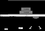
) that are evaporated at high temperatures from solid elemental sources, while the sources for CBE are in vapor phase at room temperatures. A comparison of the different processes in the growth chamber for MOCVD, MBE and CBE can be seen in figure 1.

cryoshield and a rotatable crystal
holder capable of carrying more than one wafer. The crystal holder is usually heated from the backside to temperatures of 500 to 700°C. Most setups also have RHEED equipment for the in-situ monitoring of surface superstructures on the growing surface and for measuring growth rates, and mass spectrometers for the analysis of the molecular species in the beams and the analysis of the residual gases.
The gas inlet system, which is one of the most important components of the system, controls the material beam flux. Pressure controlled systems are used most commonly. The material flux is controlled by the input pressure of the gas injection capillary. The pressure inside the chamber can be measured and controlled by a capacitance manometer. The molecular beams of gaseous source materials injectors or effusion jets that ensure a homogeneous beam profile. For some starting compounds, such as the hydrides that are the group V starting material, the hydrides have to be precracked into the injector. This is usually done by thermally decomposing with a heated metal or filament.
associated with CBE, it is important to look at physical and chemical processes associated with MBE and MOCVD as well. Figure 2 depicts those. The growth kinetics for these three techniques differ in many ways. In conventional gas source MBE, the growth rate is determined by the arrival rate of the group III atomic beams. The epitaxial growth takes place as the group III atoms impinge on the heated substrate surface, migrates into the appropriate lattice
sites and then deposits near excess group V dimers or tetramers. It is worth noting that no chemical reaction is involved at the surface since the atoms are generated by thermal evaporation
from solid elemental sources.
 In MOCVD, group III alkyls are already partially dissociated in the gas stream. These diffuse through a stagnant boundary layer that exists over the heated substrate, after which they dissociate into the atomic group III elements. These atoms then migrate to the appropriate lattice site and deposit epitaxially by associating with a group V atom that was derived from the thermal decomposition of the hydrides. The growth rate here is usually limited by the diffusion rate of the group III alkyls through the boundary layer. Gas phase reactions between the reactants have also been observed in this process.
In CBE processes, the hydrides are cracked in a high temperature injector before they reach the substrate. The temperatures are typically 100-150°C lower than they are in a similar MOCVD or MOVPE. There is also no boundary layer (such as the one in MOCVD) and molecular collisions are minimal due to the low pressure. The group V alkyls are usually supplied in excess, and the group III alkyl molecules impinge directly onto the heated substrate as in conventional MBE. The group III alkyl molecule has two options when this happens. The first option is to dissociate its three alkyl radicals by acquiring thermal energy
from the surface, and leaving behind the elemental group III atoms on the surface. The second option is to re-evaporate partially or completely undissociated. Thus, the growth rate is determined by the arrival rate of the group III alkyls at a higher substrate temperature, and by the surface pyrolysis rate at lower temperatures.
. However, it was found that using TEGa instead of TMGa led to very clean GaAs with room temperature hole concentrations between 1014 and 1016 cm-3. It has been demonstrated that the hole concentrations can be adjusted between 1014 and 1021 cm-3 by just adjusting the alkyl beam pressure and the TMGa/TEGa ratio, providing means for achieving high and controllable p-type doping of GaAs. This has been exploited for fabricating high quality heterojunction bipolar transistor
s.
Vacuum
In everyday usage, vacuum is a volume of space that is essentially empty of matter, such that its gaseous pressure is much less than atmospheric pressure. The word comes from the Latin term for "empty". A perfect vacuum would be one with no particles in it at all, which is impossible to achieve in...
system. The reactants are in the form of molecular beams of reactive gases, typically as the hydride
Hydride
In chemistry, a hydride is the anion of hydrogen, H−, or, more commonly, a compound in which one or more hydrogen centres have nucleophilic, reducing, or basic properties. In compounds that are regarded as hydrides, hydrogen is bonded to a more electropositive element or group...
or a metalorganic. The term CBE is often used interchangeably with metal-organic molecular beam epitaxy (MOMBE). The nomenclature does differentiate between the two (slightly different) processes, however. When used in the strictest sense, CBE refers to the technique in which both components are obtained from gaseous sources, while MOMBE refers to the technique in which the group III component is obtained from a gaseous source and the group V component from a solid source.
Basic principles
Chemical Beam Epitaxy was first demonstrated by W.T. Tsang in 1984. This technique was then described as a hybrid of metal-organic chemical vapor deposition (MOCVD) and molecular beam epitaxy (MBE) that exploited the advantages of both the techniques. In this initial work, InP and GaAs were grown using gaseous group III and V alkyls. While group III elements were derived from the pyrolysisPyrolysis
Pyrolysis is a thermochemical decomposition of organic material at elevated temperatures without the participation of oxygen. It involves the simultaneous change of chemical composition and physical phase, and is irreversible...
of the alkyls on the surface, the group V elements were obtained from the decomposition of the alkyls by bringing in contact with heated Tantalum
Tantalum
Tantalum is a chemical element with the symbol Ta and atomic number 73. Previously known as tantalium, the name comes from Tantalus, a character in Greek mythology. Tantalum is a rare, hard, blue-gray, lustrous transition metal that is highly corrosion resistant. It is part of the refractory...
(Ta) or Molybdenum
Molybdenum
Molybdenum , is a Group 6 chemical element with the symbol Mo and atomic number 42. The name is from Neo-Latin Molybdaenum, from Ancient Greek , meaning lead, itself proposed as a loanword from Anatolian Luvian and Lydian languages, since its ores were confused with lead ores...
(Mo) at 950-1200 °C.
Typical pressure in the gas reactor is between 102 Torr
Torr
The torr is a non-SI unit of pressure with the ratio of 760 to 1 standard atmosphere, chosen to be roughly equal to the fluid pressure exerted by a millimetre of mercury, i.e., a pressure of 1 torr is approximately equal to 1 mmHg...
and 1 atm for MOCVD. Here, the transport of gas occurs by viscous
Viscosity
Viscosity is a measure of the resistance of a fluid which is being deformed by either shear or tensile stress. In everyday terms , viscosity is "thickness" or "internal friction". Thus, water is "thin", having a lower viscosity, while honey is "thick", having a higher viscosity...
flow and chemicals reach the surface by diffusion. In contrast, gas pressures of less than 10-4 Torr are used in CBE. The gas transport now occurs as molecular beam due to the much longer mean-free paths, and the process evolves to a chemical beam deposition. It is also worth noting here that MBE employs atomic beams (such as aluminium
Aluminium
Aluminium or aluminum is a silvery white member of the boron group of chemical elements. It has the symbol Al, and its atomic number is 13. It is not soluble in water under normal circumstances....
(Al) and Gallium
Gallium
Gallium is a chemical element that has the symbol Ga and atomic number 31. Elemental gallium does not occur in nature, but as the gallium salt in trace amounts in bauxite and zinc ores. A soft silvery metallic poor metal, elemental gallium is a brittle solid at low temperatures. As it liquefies...
(Ga)) and molecular beams (such as As4
Arsenic
Arsenic is a chemical element with the symbol As, atomic number 33 and relative atomic mass 74.92. Arsenic occurs in many minerals, usually in conjunction with sulfur and metals, and also as a pure elemental crystal. It was first documented by Albertus Magnus in 1250.Arsenic is a metalloid...
and P4
Phosphorus
Phosphorus is the chemical element that has the symbol P and atomic number 15. A multivalent nonmetal of the nitrogen group, phosphorus as a mineral is almost always present in its maximally oxidized state, as inorganic phosphate rocks...
) that are evaporated at high temperatures from solid elemental sources, while the sources for CBE are in vapor phase at room temperatures. A comparison of the different processes in the growth chamber for MOCVD, MBE and CBE can be seen in figure 1.
Experimental Setup
A combination of turbomolecular and cryo pumps are used in standard UHV growth chambers. The chamber itself is equipped with a liquid nitrogenLiquid nitrogen
Liquid nitrogen is nitrogen in a liquid state at a very low temperature. It is produced industrially by fractional distillation of liquid air. Liquid nitrogen is a colourless clear liquid with density of 0.807 g/mL at its boiling point and a dielectric constant of 1.4...
cryoshield and a rotatable crystal
Crystal
A crystal or crystalline solid is a solid material whose constituent atoms, molecules, or ions are arranged in an orderly repeating pattern extending in all three spatial dimensions. The scientific study of crystals and crystal formation is known as crystallography...
holder capable of carrying more than one wafer. The crystal holder is usually heated from the backside to temperatures of 500 to 700°C. Most setups also have RHEED equipment for the in-situ monitoring of surface superstructures on the growing surface and for measuring growth rates, and mass spectrometers for the analysis of the molecular species in the beams and the analysis of the residual gases.
The gas inlet system, which is one of the most important components of the system, controls the material beam flux. Pressure controlled systems are used most commonly. The material flux is controlled by the input pressure of the gas injection capillary. The pressure inside the chamber can be measured and controlled by a capacitance manometer. The molecular beams of gaseous source materials injectors or effusion jets that ensure a homogeneous beam profile. For some starting compounds, such as the hydrides that are the group V starting material, the hydrides have to be precracked into the injector. This is usually done by thermally decomposing with a heated metal or filament.
Growth Kinetics
In order to better understand the growth kineticsChemical kinetics
Chemical kinetics, also known as reaction kinetics, is the study of rates of chemical processes. Chemical kinetics includes investigations of how different experimental conditions can influence the speed of a chemical reaction and yield information about the reaction's mechanism and transition...
associated with CBE, it is important to look at physical and chemical processes associated with MBE and MOCVD as well. Figure 2 depicts those. The growth kinetics for these three techniques differ in many ways. In conventional gas source MBE, the growth rate is determined by the arrival rate of the group III atomic beams. The epitaxial growth takes place as the group III atoms impinge on the heated substrate surface, migrates into the appropriate lattice
Crystal structure
In mineralogy and crystallography, crystal structure is a unique arrangement of atoms or molecules in a crystalline liquid or solid. A crystal structure is composed of a pattern, a set of atoms arranged in a particular way, and a lattice exhibiting long-range order and symmetry...
sites and then deposits near excess group V dimers or tetramers. It is worth noting that no chemical reaction is involved at the surface since the atoms are generated by thermal evaporation
Evaporation
Evaporation is a type of vaporization of a liquid that occurs only on the surface of a liquid. The other type of vaporization is boiling, which, instead, occurs on the entire mass of the liquid....
from solid elemental sources.
In CBE processes, the hydrides are cracked in a high temperature injector before they reach the substrate. The temperatures are typically 100-150°C lower than they are in a similar MOCVD or MOVPE. There is also no boundary layer (such as the one in MOCVD) and molecular collisions are minimal due to the low pressure. The group V alkyls are usually supplied in excess, and the group III alkyl molecules impinge directly onto the heated substrate as in conventional MBE. The group III alkyl molecule has two options when this happens. The first option is to dissociate its three alkyl radicals by acquiring thermal energy
Thermal energy
Thermal energy is the part of the total internal energy of a thermodynamic system or sample of matter that results in the system's temperature....
from the surface, and leaving behind the elemental group III atoms on the surface. The second option is to re-evaporate partially or completely undissociated. Thus, the growth rate is determined by the arrival rate of the group III alkyls at a higher substrate temperature, and by the surface pyrolysis rate at lower temperatures.
Selective Growth at Low Temperatures
Selective growth through dielectric masking is readily achieved using CBE as compared to its parent techniques of MBE and MOCVD. Selective growth is hard to achieve using elemental source MBE because group III atoms do not desorb readily after they are adsorbed. With chemical sources, the reactions associated with the growth rate are faster on the semiconductor surface than on the dielectric layer. No group III element can, however, arrive at the dielectric surface in CBE due to the absence of any gas phase reactions. Also, it is easier for the impinging group III metalorganic molecules to desorb in the absence of the boundary layer. This makes it easier to perform selective epitaxy using CBE and at lower temperatures, compared to MOCVD or MOVPE.p-type Doping
It was observed that using TMGa for the CBE of GaAs led to high p-type background doping (1020 cm-3) due to incorporated carbonCarbon
Carbon is the chemical element with symbol C and atomic number 6. As a member of group 14 on the periodic table, it is nonmetallic and tetravalent—making four electrons available to form covalent chemical bonds...
. However, it was found that using TEGa instead of TMGa led to very clean GaAs with room temperature hole concentrations between 1014 and 1016 cm-3. It has been demonstrated that the hole concentrations can be adjusted between 1014 and 1021 cm-3 by just adjusting the alkyl beam pressure and the TMGa/TEGa ratio, providing means for achieving high and controllable p-type doping of GaAs. This has been exploited for fabricating high quality heterojunction bipolar transistor
Transistor
A transistor is a semiconductor device used to amplify and switch electronic signals and power. It is composed of a semiconductor material with at least three terminals for connection to an external circuit. A voltage or current applied to one pair of the transistor's terminals changes the current...
s.
Advantages and Disadvantages of CBE
CBE offers many other advantages over its parent techniques of MOCVD and MBE, some of which are listed below:Advantages over MBE
- Easier multiwafer scaleup: Substrate rotation is required for uniformity in thickness and conformity since MBE has individual effusion cells for each element. Large effusion cells and efficient heat dissipation make multiwafer scaleup more difficult.
- Better for production environment: Instant flux response due to precision electronic control flow.
- Absence of oval defects: These oval defects generally arise from micro-droplets of Ga or In spit out from high temperature effusion cells. These defects vary in size and density system-to-system and time-to-time.
Advantages over MOCVD
- Easy implementation of in-situ diagnostic instruments such as RHEED.
- Compatibility with other high vacuum thin-film processing methods, such as metal evaporation and ion implantation.
Shortcomings of CBE
- More pumping required compared to MOCVD.
- Composition control can be difficult when growing GaInAs. Incorporation of In from TMIn is significantly larger than that for Ga from TEGa at temperatures around 600°C.
- High carbon incorporation for GaAlAs.
See also
- EpitaxyEpitaxyEpitaxy refers to the deposition of a crystalline overlayer on a crystalline substrate, where the overlayer is in registry with the substrate. In other words, there must be one or more preferred orientations of the overlayer with respect to the substrate for this to be termed epitaxial growth. The...
- Molecular beam epitaxyMolecular beam epitaxyMolecular beam epitaxy is one of several methods of depositing single crystals. It was invented in the late 1960s at Bell Telephone Laboratories by J. R. Arthur and Alfred Y. Cho.-Method:...
- MOVPE
- Compound semiconductorCompound semiconductorA compound semiconductor is a semiconductor compound composed of elements from two or more different groups of the periodic table . These semiconductors typically form in groups 13-16 ,...
- Chemical Vapor DepositionChemical vapor depositionChemical vapor deposition is a chemical process used to produce high-purity, high-performance solid materials. The process is often used in the semiconductor industry to produce thin films. In a typical CVD process, the wafer is exposed to one or more volatile precursors, which react and/or...
- MetalorganicsMetalorganicsMetalorganic compounds are a class of chemical compounds that contain metals and organic ligands. Metalorganic compounds are used extensively in materials science in applications such as metalorganic vapour phase epitaxy or sol-gel processing using alkoxides...
- Thin-film deposition
- RHEEDRHEEDReflection high-energy electron diffraction is a technique used to characterize the surface of crystalline materials. RHEED systems gather information only from the surface layer of the sample, which distinguishes RHEED from other materials characterization methods that also rely on diffraction of...