

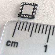
QFN
Encyclopedia
Integrated circuit
An integrated circuit or monolithic integrated circuit is an electronic circuit manufactured by the patterned diffusion of trace elements into the surface of a thin substrate of semiconductor material...
s to printed circuit board
Printed circuit board
A printed circuit board, or PCB, is used to mechanically support and electrically connect electronic components using conductive pathways, tracks or signal traces etched from copper sheets laminated onto a non-conductive substrate. It is also referred to as printed wiring board or etched wiring...
s. Flat no-leads, also known as MicroLeadFrame
MicroLeadFrame
Amkor's MicroLeadFrame is a near CSP plastic encapsulated package with a copper leadframe substrate. This package uses perimeter lands on the bottom of the package to provide electrical contact to the...
, is a surface-mount technology
Surface-mount technology
Surface mount technology is a method for constructing electronic circuits in which the components are mounted directly onto the surface of printed circuit boards . An electronic device so made is called a surface mount device...
, one of several package technologies that connect IC
Integrated circuit
An integrated circuit or monolithic integrated circuit is an electronic circuit manufactured by the patterned diffusion of trace elements into the surface of a thin substrate of semiconductor material...
s to the surfaces of PCB
Printed circuit board
A printed circuit board, or PCB, is used to mechanically support and electrically connect electronic components using conductive pathways, tracks or signal traces etched from copper sheets laminated onto a non-conductive substrate. It is also referred to as printed wiring board or etched wiring...
s without through-holes
Through-hole technology
Through-hole technology, also spelled "thru-hole", refers to the mounting scheme used for electronic components that involves the use of leads on the components that are inserted into holes drilled in printed circuit boards and soldered to pads on the opposite side either by manual assembly by...
. Flat no-lead is a near chip scale package
Chip scale package
A chip scale package is a type of integrated circuit chip carrier.Originally, CSP was the acronym for chip-size packaging. Since only a few packages are chip size, the meaning of the acronym was adapted to chip-scale packaging...
plastic encapsulated package made with a planar copper lead frame substrate. Perimeter lands on the package bottom provide electrical connections to the PCB
Printed circuit board
A printed circuit board, or PCB, is used to mechanically support and electrically connect electronic components using conductive pathways, tracks or signal traces etched from copper sheets laminated onto a non-conductive substrate. It is also referred to as printed wiring board or etched wiring...
. Flat no-lead packages include an exposed thermal pad to improve heat transfer out of the IC
Integrated circuit
An integrated circuit or monolithic integrated circuit is an electronic circuit manufactured by the patterned diffusion of trace elements into the surface of a thin substrate of semiconductor material...
(into the PCB). Heat transfer can be further facilitated by metal vias
Via (electronics)
A via is a vertical electrical connection between different layers of conductors in a physical electronic circuit.- In IC :In integrated circuit design, a via is a small opening in an insulating oxide layer that allows a conductive connection between different layers. A via on an integrated circuit...
in the thermal pad. The QFN package is similar to the quad-flat package
QFP
A QFP or Quad Flat Package is a surface mount integrated circuit package with leads extending from each of the four sides. Socketing such packages is rare and hole mounting is not possible. Versions ranging from 32 to 304 pins with a pitch ranging from 0.4 to 1.0 mm are common...
, and a ball grid array
Ball grid array
A ball grid array is a type of surface-mount packaging used for integrated circuits.- Description :The BGA is descended from the pin grid array , which is a package with one face covered with pins in a grid pattern. These pins conduct electrical signals from the integrated circuit to the printed...
.
Flat No lead Cross section
The figure shows the cross section of a Flat No lead package with a lead frame and wire bondingWire bonding
Wire bonding is the primary method of making interconnections between an integrated circuit and a printed circuit board during semiconductor device fabrication. Although less common, wire bonding can be used to connect an IC to other electronics or to connect from one PCB to another...
. There are two types of body designs, punch singulation and saw singulation. Saw singulation cuts a large set of packages in parts. In punch singulation, a single package is moulded into shape. The cross section shows a saw-singulated body with an attached thermal head pad. The lead frame is made of copper alloy and a thermally conductive adhesive is used for attaching the silicon die to the thermal pad. The silicon die is electrically connected to the lead frame by 1-2mil diameter gold wires
Wire bonding
Wire bonding is the primary method of making interconnections between an integrated circuit and a printed circuit board during semiconductor device fabrication. Although less common, wire bonding can be used to connect an IC to other electronics or to connect from one PCB to another...
.
The pads of a saw-singulated package can either be completely under the package, or they can fold around the edge of the package.
Different Types of QFNs
Two types of QFN packages are common: air-cavity QFNs, with an air cavity designed into the package, and plastic-moulded QFNs with air in the package minimized.Less-expensive plastic-moulded QFNs usually limited to applications up to ~2–3 GHz. It is usually composed of just 2 parts, a plastic compound and copper lead frame, and does not come with a lid.
In contrast, the air-cavity QFN is usually made up of 3 parts; a copper leadframe, plastic-moulded body (open, and not sealed), and either a ceramic or plastic lid. It is usually more expensive due to its construction, and can be used for microwave applications up to 20–25 GHz.
QFN packages can have a single row of contacts or a double row of contacts.
Advantages
This package offers variety of benefits including reduced lead inductance, a small sized "near chip scale" footprint, thin profile and low weight. It also uses perimeter I/O pads to ease PCB trace routing, and the exposed copper die-pad technology offers good thermal and electrical performance. These features make the QFN an ideal choice for many new applications where size, weight, and thermal and electrical performance are important.Disadvantages
The small size of the exposed contacts, and the large area of exposed thermal pad makes it easy for small parts, such as 3x3mm DFN packages, to float on the pool of molten solder under the thermal pad during assembly. This causes the parts to make no contact to the printed circuit board pads in some instances. Due to the excellent thermal characteristics of this mounting package, it is very hard to rework the device, as hot air reflow typically does not offer enough heat to the thermal pad without damage to surrounding board material or parts. Oxidation of the exposed chip contact pads after being exposed to a reflow oven during initial assembly makes solder wetting to them during rework quite difficult. Additionally there is no clearance for a soldering pencil to reflow pads under the chip if touch up is desired. Sometimes contact can be made up the sides of the DFN package contact pads, but this does not work well in practice.Comparison to other packages
The QFN package is similar to the Quad Flat PackageQFP
A QFP or Quad Flat Package is a surface mount integrated circuit package with leads extending from each of the four sides. Socketing such packages is rare and hole mounting is not possible. Versions ranging from 32 to 304 pins with a pitch ranging from 0.4 to 1.0 mm are common...
, but the leads do not extend out from the package sides. It is hence difficult to hand-solder a QFN package.
A QFN package is very similar to a Ball grid array
Ball grid array
A ball grid array is a type of surface-mount packaging used for integrated circuits.- Description :The BGA is descended from the pin grid array , which is a package with one face covered with pins in a grid pattern. These pins conduct electrical signals from the integrated circuit to the printed...
(BGA), except that the QFN uses landing pads, and solder paste
Solder paste
Solder paste sometimes refers to soldering flux that does not contain solder.Solder paste is used to connect the leads of integrated chip packages to attachment points in the circuit patterns on a printed circuit board...
is required to mount a QFN package onto the PCB. A BGA-package does not require any solder as the balls will melt and make contact with the PCB.
Variants
Different manufacturers use different names for this package: ML (micro-leadframe) versus FN (flat no-lead), in addition there are versions with pads on all four sides (quad) and pads on just two sides (dual), and various thickness varying between 0.9–1.0 mm for normal packages and 0.4 mm for extreme thin. Abbreviations include:| Package | Manufacturer | |
|---|---|---|
| DFN | dual flat no-lead package | |
| TDFN | thin dual flat no-lead package | |
| UTDFN | ultra-thin dual flat no-lead package | |
| XDFN | extremely thin dual flat no-lead package | |
| QFN | quad flat no-lead package | |
| QFN-TEP | quad flat no-lead package with top-exposed pad | |
| TQFN | thin quad flat no-lead package | |
| LLP | leadless leadframe package | National Semiconductor National Semiconductor National Semiconductor was an American semiconductor manufacturer, that specialized in analog devices and subsystems,formerly headquartered in Santa Clara, California, USA. The products of National Semiconductor included power management circuits, display drivers, audio and operational amplifiers,... |
| LPCC | leadless plastic chip carrier | ASAT Holdings |
| MLF | micro-leadframe | Amkor Technology |
| MLPD | micro-leadframe package dual | |
| MLPM | micro-leadframe package micro | |
| MLPQ | micro-leadframe package quad | |
| DRMLF | dual-row micro-leadframe package |