

Piezoresponse Force Microscopy
Encyclopedia
Piezoresponse force microscopy (PFM) is a variant of atomic force microscopy (AFM) that allows imaging and manipulation of ferroelectric domains. This is achieved by bringing a sharp conductive probe into contact with a ferroelectric surface (or piezoelectric material) and applying an alternating current
(AC) bias to the probe tip in order to excite deformation of the sample through the converse piezoelectric effect (CPE). The resulting deflection of the probe cantilever is detected through standard split photodiode
detector methods and then demodulated by use of a lock-in amplifier
(LiA). In this way topography and ferroelectric domains can be imaged simultaneously with high resolution.
Consider that a static or DC voltage applied to a piezoelectric surface will produce a displacement but as applied fields are quite low and the piezoelectric tensor coefficients are relatively small then the physical displacement will also be small such that it is below the level of possible detection of the system. Take as an example, the d33 piezoelectric tensor coefficient of BaTiO3, it has a value of 85.6 pm
V−1
meaning that applying 1 V across the material results in a displacement of 85.6 pm or 0.0856 nm
, a minute cantilever displacement even for the high precision of AFM deflection detection. In order to separate this low level signal from random noise a lock-in technique is used wherein a modulated voltage reference signal,
of frequency ω and amplitude Vac is applied to the tip giving rise to an oscillatory deformation of the sample surface,
from the equilibrium position d0 with amplitude D, and an associated phase difference φ. The resulting movement of the cantilever is detected by the photodiode and so an oscillating surface displacement is converted into an oscillating voltage. A lock-in-amplifier (LiA) is then able to retrieve the amplitude and phase of the CPE induced surface deformation by the process outlined below.
will create a resultant strain
which in turn leads to a physical deformation of the material. This effect can be described through the constitutive equations. The CPE can be written as
where Xi is the strain tensor, dki is the piezoelectric tensor, and Ek is the electric field. If the piezoelectric tensor is considered to be that of the tetragonal crystal system (that of BaTiO3) then it is
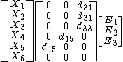
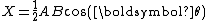
such that the equation will lead to the strain components for an applied field. If the field is applied exclusively in one direction i.e. E3 for example, then the resulting strain components are: d31E3, d31E3, d33E3
Thus for an electric field applied along the c-axis of BaTiO3 i.e. E3, then the resulting deformation of the crystal will be an elongation along the c-axis and an axially symmetric contraction along the other orthogonal directions. PFM uses the effect of this deformation to detect domains and also to determine their orientation.
, gold
, tungsten
and even conductive diamond
.
and is done in a number of easy steps. The reference signal , and input signal,
  , are multiplied together to give the demodulator output,

where A is the input signal Amplitude and B is the reference signal Amplitude, ω is the frequency of both the reference and input signals, and φ is any phase shift between the two signals.
The above equation has an AC component at twice the frequency of the original signals (second term) and a DC component (first term) whose value is related to both the amplitude and phase of the input signal. The demodulator output is sent through a low-pass filter to remove the 2ω component and leave the DC component then the signal is integrated over a period of time defined as the Time Constant, τLiA which is a user-definable parameter. Several different outputs are commonly available from a LiA: X output is the demodulator output and Y is the second demodulator output which is shifted by 90° in reference to the first output, together they hold both the phase, θ, and magnitude, R, information and are given by
 and
and

However, phase and amplitude of the input signal can also be calculated and outputted from the LiA if desired, so that the full amount of information is available. The phase output can be determined from the following equation:
The magnitude is then given by:

This allows R to be calculated even if the input signal differs in phase from the reference signal.
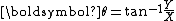
For polar components orientated such that they are parallel to the electric field the resulting oscillating movement will be entirely in-phase with the modulated electric field but for an anti-parallel alignment the motion will be 180° out-of-phase. In this way it is possible to determine the orientation of the vertical components of polarisation from analysis of the phase information, φ, contained in the input signal, readily available after demodulation in the LiA, when using the VPFM mode. In a similar sense the orientations of in-plane polar components can also be determined from the phase difference when using the LPFM mode. The amplitude of the piezoresponse of either VPFM or LPFM is also given by the LiA, in the form of the magnitude, R.
(KTP) as imaged by VPFM. In the image piezoresponse amplitude can be seen where dark areas represent the zero amplitude that is expected at domain boundaries where the unit cell is cubic i.e. centrosymmetric and so therefore not ferroelectric. On the left hand side piezoresponse phase can be seen where the measured phase changes to show the out-of-plane components that are pointing out of the screen, white areas, and into the screen, dark areas. The scan area is 20×10 µm2. Below each scan is the relevant cross-section that shows in arbitrary units the PR amplitude and phase.
. As such there exists a resonance as a function of driving frequency. This effect has been exploited in PFM to provide an enhancement in the PR signal, thus allowing for a higher signal-to-noise or similar signal-to-noise at lower driving bias amplitude. Typically this contact resonance is in the kilo- to mega-hertz
range which is several times higher in frequency than the first free harmonic in air of the cantilever used. However a drawback is that the contact resonance is dependent not only on the dynamic response of the cantilever but also on the elastic modulus
of the sample material immediately in contact with the probe tip and so therefore can change during scanning over different areas. This leads to a change in the measured PR amplitude and so is undesirable. One method of bypassing the inherent disadvantages of contact resonance PFM is to change the driving frequency in order to shadow or track the changes in the frequency of the contact resonance. This feature as developed by Asylum Research called dual drequency resonance tracking (DFRT) uses two limit frequencies on either side of the contact resonance peak and so can sense changes in the peak position. It is then possible to adapt the AC bias driving frequency correspondingly in order to maintain the signal boost that results from the contact resonance.
loop that can be analysed to obtain information about the sample properties. A series of hysteresis loops are acquired across the sample surface in order to map the switching characteristics as a function of position. In this way an image representing switching properties such as coercive voltage, remnant polarisation, imprint and work of switching amongst others can be displayed in which each pixel displays the desired data from the hysteresis loop acquired at that point. This allows spatial analysis of switching properties to be compared with sample topography.
Alternating current
In alternating current the movement of electric charge periodically reverses direction. In direct current , the flow of electric charge is only in one direction....
(AC) bias to the probe tip in order to excite deformation of the sample through the converse piezoelectric effect (CPE). The resulting deflection of the probe cantilever is detected through standard split photodiode
Photodiode
A photodiode is a type of photodetector capable of converting light into either current or voltage, depending upon the mode of operation.The common, traditional solar cell used to generateelectric solar power is a large area photodiode....
detector methods and then demodulated by use of a lock-in amplifier
Lock-in amplifier
A lock-in amplifier is a type of amplifier that can extract a signal with a known carrier wave from an extremely noisy environment . It is essentially a homodyne with an extremely low pass filter...
(LiA). In this way topography and ferroelectric domains can be imaged simultaneously with high resolution.
General overview
Piezoresponse force microscopy is a technique which since its inception and first implementation has steadily attracted more and more interest. This is due in large part to the many benefits and few drawbacks that PFM offers researchers in varying fields from ferroelectrics, semiconductors and even biology. In its most common format PFM allows for identification of domains from relatively large scale e.g. 100×100 µm2 scans right down to the nanoscale with the added advantage of simultaneous imaging of sample surface topography. Also possible is the ability to switch regions of ferroelectric domains with the application of a sufficiently high bias to the probe which opens up the opportunity of investigating domain formation on nanometre length scales with nanosecond time resolution. Many recent advances have expanded the list of applications for PFM and further increased this powerful technique. Indeed what started as a user modified AFM has now attracted the attention of the major SPM manufacturers so much so that in fact many now supply ‘ready-made’ systems specifically for PFM each with novel features for research. This is testament to the growth of the field and reflects the numbers of users throughout the scientific world who are at the forefront of scientific research.Consider that a static or DC voltage applied to a piezoelectric surface will produce a displacement but as applied fields are quite low and the piezoelectric tensor coefficients are relatively small then the physical displacement will also be small such that it is below the level of possible detection of the system. Take as an example, the d33 piezoelectric tensor coefficient of BaTiO3, it has a value of 85.6 pm
Picometre
A picometre is a unit of length in the metric system, equal to one trillionth, i.e. of a metre, which is the current SI base unit of length...
V−1
Volt
The volt is the SI derived unit for electric potential, electric potential difference, and electromotive force. The volt is named in honor of the Italian physicist Alessandro Volta , who invented the voltaic pile, possibly the first chemical battery.- Definition :A single volt is defined as the...
meaning that applying 1 V across the material results in a displacement of 85.6 pm or 0.0856 nm
Nanometre
A nanometre is a unit of length in the metric system, equal to one billionth of a metre. The name combines the SI prefix nano- with the parent unit name metre .The nanometre is often used to express dimensions on the atomic scale: the diameter...
, a minute cantilever displacement even for the high precision of AFM deflection detection. In order to separate this low level signal from random noise a lock-in technique is used wherein a modulated voltage reference signal,

of frequency ω and amplitude Vac is applied to the tip giving rise to an oscillatory deformation of the sample surface,

from the equilibrium position d0 with amplitude D, and an associated phase difference φ. The resulting movement of the cantilever is detected by the photodiode and so an oscillating surface displacement is converted into an oscillating voltage. A lock-in-amplifier (LiA) is then able to retrieve the amplitude and phase of the CPE induced surface deformation by the process outlined below.
Converse piezoelectric effect
The converse piezoelectric effect (CPE) describes how an applied electric fieldElectric field
In physics, an electric field surrounds electrically charged particles and time-varying magnetic fields. The electric field depicts the force exerted on other electrically charged objects by the electrically charged particle the field is surrounding...
will create a resultant strain
Deformation (mechanics)
Deformation in continuum mechanics is the transformation of a body from a reference configuration to a current configuration. A configuration is a set containing the positions of all particles of the body...
which in turn leads to a physical deformation of the material. This effect can be described through the constitutive equations. The CPE can be written as

where Xi is the strain tensor, dki is the piezoelectric tensor, and Ek is the electric field. If the piezoelectric tensor is considered to be that of the tetragonal crystal system (that of BaTiO3) then it is
such that the equation will lead to the strain components for an applied field. If the field is applied exclusively in one direction i.e. E3 for example, then the resulting strain components are: d31E3, d31E3, d33E3
Thus for an electric field applied along the c-axis of BaTiO3 i.e. E3, then the resulting deformation of the crystal will be an elongation along the c-axis and an axially symmetric contraction along the other orthogonal directions. PFM uses the effect of this deformation to detect domains and also to determine their orientation.
Conductive probe
The most important property of the probe for use in PFM is that it should be conducting. This is generally required in order to provide a means of applying a bias to the sample, and can be achieved through manufacturing standard silicon probes and coating them in a conductive material. Common coatings are platinumPlatinum
Platinum is a chemical element with the chemical symbol Pt and an atomic number of 78. Its name is derived from the Spanish term platina del Pinto, which is literally translated into "little silver of the Pinto River." It is a dense, malleable, ductile, precious, gray-white transition metal...
, gold
Gold
Gold is a chemical element with the symbol Au and an atomic number of 79. Gold is a dense, soft, shiny, malleable and ductile metal. Pure gold has a bright yellow color and luster traditionally considered attractive, which it maintains without oxidizing in air or water. Chemically, gold is a...
, tungsten
Tungsten
Tungsten , also known as wolfram , is a chemical element with the chemical symbol W and atomic number 74.A hard, rare metal under standard conditions when uncombined, tungsten is found naturally on Earth only in chemical compounds. It was identified as a new element in 1781, and first isolated as...
and even conductive diamond
Diamond
In mineralogy, diamond is an allotrope of carbon, where the carbon atoms are arranged in a variation of the face-centered cubic crystal structure called a diamond lattice. Diamond is less stable than graphite, but the conversion rate from diamond to graphite is negligible at ambient conditions...
.
Lock-in amplifier
In the general case a LiA ‘compares’ an input signal against that of a reference signal (either generated internally or supplied by an external function generator) in order to separate the information contained in the input signal at the frequency of the reference signal. This is called demodulationDemodulation
Demodulation is the act of extracting the original information-bearing signal from a modulated carrier wave.A demodulator is an electronic circuit that is used to recover the information content from the modulated carrier wave.These terms are traditionally used in connection with radio receivers,...
and is done in a number of easy steps. The reference signal
, and input signal, , are multiplied together to give the demodulator output,where A is the input signal Amplitude and B is the reference signal Amplitude, ω is the frequency of both the reference and input signals, and φ is any phase shift between the two signals.
The above equation has an AC component at twice the frequency of the original signals (second term) and a DC component (first term) whose value is related to both the amplitude and phase of the input signal. The demodulator output is sent through a low-pass filter to remove the 2ω component and leave the DC component then the signal is integrated over a period of time defined as the Time Constant, τLiA which is a user-definable parameter. Several different outputs are commonly available from a LiA: X output is the demodulator output and Y is the second demodulator output which is shifted by 90° in reference to the first output, together they hold both the phase, θ, and magnitude, R, information and are given by
andHowever, phase and amplitude of the input signal can also be calculated and outputted from the LiA if desired, so that the full amount of information is available. The phase output can be determined from the following equation:
The magnitude is then given by:
This allows R to be calculated even if the input signal differs in phase from the reference signal.
Differentiating vertical and lateral PFM signals
A basic interpretation of PFM (which is generally accepted) identifies that two modes of imaging are possible, one that is sensitive to out-of-plane and one to in-plane piezoresponse, termed, vertical and lateral PFM (VPFM and LPFM) respectively. The separation of these components is possible through the use of a split photodiode detector, standard to all optical detection AFM systems. In this setup the detector is split into quadrants, nominally A, B, C and D. The centre of the entire detector outputs 0 V but as the laser spot moves a radial distance from this centre point the magnitude of the outputted voltage will increase linearly. A vertical deflection can be defined as {(A+B)-(C+D)}/(ABCD) so that now positive and negative voltages are ascribed to positive and negative cantilever vertical displacements. Similarly a lateral deflection is defined as {(B+D)-(A+C)}/(ABCD) to describe positive and negative torsional movements of the cantilever. So VPFM will utilise the vertical deflection signal from the photodiode detector so will only be sensitive to out-of-plane polar components and LPFM will utilise the lateral deflection signal from the photodiode and will only be sensitive to in-plane polar components.For polar components orientated such that they are parallel to the electric field the resulting oscillating movement will be entirely in-phase with the modulated electric field but for an anti-parallel alignment the motion will be 180° out-of-phase. In this way it is possible to determine the orientation of the vertical components of polarisation from analysis of the phase information, φ, contained in the input signal, readily available after demodulation in the LiA, when using the VPFM mode. In a similar sense the orientations of in-plane polar components can also be determined from the phase difference when using the LPFM mode. The amplitude of the piezoresponse of either VPFM or LPFM is also given by the LiA, in the form of the magnitude, R.
Examples of PFM imaging
The image shows periodically poled 180° domains in potassium titanyl phosphatePotassium titanyl phosphate
Potassium titanyl phosphate or KTP is a nonlinear optical material which is commonly used for frequency doubling diode pumped solid-state lasers such as Nd:YAG and other neodymium-doped lasers. The material has a relatively high optical damage threshold , a great optical nonlinearity and excellent...
(KTP) as imaged by VPFM. In the image piezoresponse amplitude can be seen where dark areas represent the zero amplitude that is expected at domain boundaries where the unit cell is cubic i.e. centrosymmetric and so therefore not ferroelectric. On the left hand side piezoresponse phase can be seen where the measured phase changes to show the out-of-plane components that are pointing out of the screen, white areas, and into the screen, dark areas. The scan area is 20×10 µm2. Below each scan is the relevant cross-section that shows in arbitrary units the PR amplitude and phase.
PFM applied to biological materials
PFM has been successfully applied to a range of biological materials such as teeth, bone, and single collagen fibrils. It has been hypothesized that the endogenous peizoelectricity in these materials may be relevant in their mechanobiology. For example, using PFM it has been shown that a single collagen fibril as small as 100 nm behaves predominantly as a shear piezoelectric materials with an effective piezoelectric constant of ~1 pm/V.Advanced PFM modes
Several additions have been made to PFM that substantially increase the flexibility of the technique to probe nanoscale features.Stroboscopic PFM
Stroboscopic PFM allows for time resolved imaging of switching in pseudo real-time. A voltage pulse of amplitude much higher than the coercive voltage of the sample but shorter in duration than the characteristic switching time is applied to the sample and subsequently imaged. Further pulses with the same amplitude but longer in time are then applied with regular PFM imaging at the intervals. In this way a series of images showing the switching of the sample can be obtained. Typical pulses are of tens of nanoseconds in duration and are therefore capable of resolving the first nucleation sites of domain reversal and then observing how these sites evolve.Contact resonance PFM
Remembering that in PFM an AC bias of a certain frequency causes a deformation of the sample material at that same frequency the system can be considered as a driven harmonic oscillatorHarmonic oscillator
In classical mechanics, a harmonic oscillator is a system that, when displaced from its equilibrium position, experiences a restoring force, F, proportional to the displacement, x: \vec F = -k \vec x \, where k is a positive constant....
. As such there exists a resonance as a function of driving frequency. This effect has been exploited in PFM to provide an enhancement in the PR signal, thus allowing for a higher signal-to-noise or similar signal-to-noise at lower driving bias amplitude. Typically this contact resonance is in the kilo- to mega-hertz
Hertz
The hertz is the SI unit of frequency defined as the number of cycles per second of a periodic phenomenon. One of its most common uses is the description of the sine wave, particularly those used in radio and audio applications....
range which is several times higher in frequency than the first free harmonic in air of the cantilever used. However a drawback is that the contact resonance is dependent not only on the dynamic response of the cantilever but also on the elastic modulus
Elastic modulus
An elastic modulus, or modulus of elasticity, is the mathematical description of an object or substance's tendency to be deformed elastically when a force is applied to it...
of the sample material immediately in contact with the probe tip and so therefore can change during scanning over different areas. This leads to a change in the measured PR amplitude and so is undesirable. One method of bypassing the inherent disadvantages of contact resonance PFM is to change the driving frequency in order to shadow or track the changes in the frequency of the contact resonance. This feature as developed by Asylum Research called dual drequency resonance tracking (DFRT) uses two limit frequencies on either side of the contact resonance peak and so can sense changes in the peak position. It is then possible to adapt the AC bias driving frequency correspondingly in order to maintain the signal boost that results from the contact resonance.
Switching spectroscopy (SS) PFM
In this technique the area underneath the PFM tip is switched with simultaneous acquisition of a hysteresisHysteresis
Hysteresis is the dependence of a system not just on its current environment but also on its past. This dependence arises because the system can be in more than one internal state. To predict its future evolution, either its internal state or its history must be known. If a given input alternately...
loop that can be analysed to obtain information about the sample properties. A series of hysteresis loops are acquired across the sample surface in order to map the switching characteristics as a function of position. In this way an image representing switching properties such as coercive voltage, remnant polarisation, imprint and work of switching amongst others can be displayed in which each pixel displays the desired data from the hysteresis loop acquired at that point. This allows spatial analysis of switching properties to be compared with sample topography.
Advantages
- High resolution on the nanometre scale
- Simultaneous acquisition of topography and piezoresponse
- Allows manipulation of ferroelectric domains
- Non-destructive
- Little sample preparation required
Disadvantages
- Scans can be slow, e.g. tens of minutes
- Tip wear changes surface interaction and can affect contrast
- Limited to lateral range of AFM i.e. approximately 100×100 µm2