

Low-energy electron microscopy
Encyclopedia
Low-energy electron microscopy, or LEEM, is an analytical surface science technique invented by Ernst Bauer in 1962, however, not fully developed (by Ernst Bauer and Wolfgang Telieps) until 1985. LEEM is a technique used by surface scientists
to image atomically clean surfaces, atom-surface interactions, and thin (crystalline) films. In LEEM, high-energy electrons (15-20 keV) are emitted from an electron gun
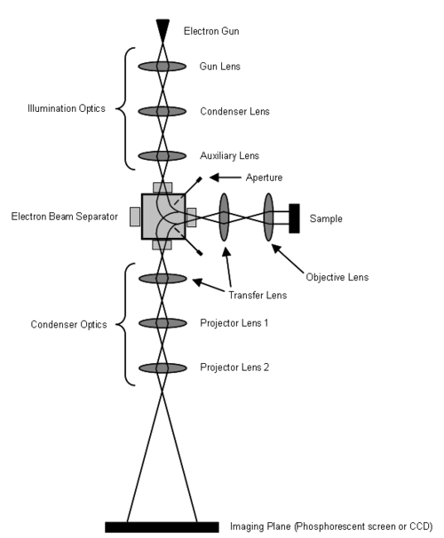
, focused using a set of condenser optics, and sent through a magnetic beam deflector (usually 60˚ or 90˚). The “fast” electrons travel through an objective lens and begin decelerating to low energies (1-100 eV) near the sample surface because the sample is held at a potential near that of the gun. The low-energy electrons are now termed “surface-sensitive” and the near-surface sampling depth can be varied by tuning the energy of the incident electrons (difference between the sample and gun potentials minus the work functions of the sample and system). The low-energy elastically backscattered electrons travel back through the condenser lens, reaccelerate to the gun voltage (because the condenser lens is grounded), and pass through the beam separator again. However, now the electrons travel away from the condenser optics and into the projector lenses. Imaging of the back focal plane of the objective lens into the object plane of the projector lens (using an intermediate lens) produces a diffraction pattern (low-energy electron diffraction, LEED) at the imaging plane and recorded in a number of different ways. The intensity distribution of the diffraction
pattern will depend on the periodicity at the sample surface and is a direct result of the wave nature of the electrons. One can produce individual images of the diffraction pattern spot intensities by turning off the intermediate lens and inserting a contrast aperture in the back focal plane of the objective lens (or, in state-of-the-art instruments, in the center of the separator, as chosen by the excitation of the objective lens), thus allowing for real-time observations of dynamic processes at surfaces. Such phenomena include (but are not limited to): tomography, phase transitions, adsorption, reaction, segregation, thin film growth, etching, strain relief, sublimation, and magnetic microstructure. These investigations are only possible because of the accessibility of the sample; allowing for a wide variety of in situ studies over a wide temperature range.
 LEEM differs from conventional electron microscopies in four main ways:
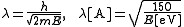
Scientists use inverse space to describe the periodicity of the lattice and the interaction of the plane wave with the sample surface. In inverse (or "k-space") space, the wave vector of the incident and scattered waves are and
and  , respectively,
and constructive interference occurs at the Laue condition:
where (h,k,l) is a set of integers and
is a vector of the reciprocal lattice.
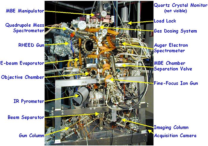
 A typical LEEM setup consists of (see figure):
1. Electron gun
, used to generate electrons by way of thermionic or field emission from a source tip. In thermionic emission, electrons escape a source tip (usually made of LaB6) by resistive heating and application of an electric field to effectively lower the energy needed for electrons to escape the surface. Once sufficient thermal vibrational energy is attained electrons may overcome this electrostatic energy barrier, allowing them to travel into vacuum and accelerate down the lens column to the gun potential (because the lenses are at ground). In field emission, rather than heating the tip to vibrationally excite electrons from the surface, the source tip (usually tungsten) is sharpened to a small point such that when large electric fields are applied, they concentrate at the tip, lowering the barrier to escape the surface as well as making tunneling of electrons from the tip to vacuum level more feasible.
2. Condenser/illumination optics, used to focus electrons leaving the electron gun and manipulate and/or translate the illumination electron beam. Electromagnetic quadrupole electron lenses are used, the number of which depends on how much resolution and focusing flexibility the designer wishes. However, the ultimate resolution of LEEM is usually determined by that of the objective lens.
3. Illumination beam aperture allows researchers to control the area of the specimen which is illuminated (LEEM’s version of electron microscopy’s “selected area diffraction”, termed microdiffraction) and is located in the beam separator on the illumination side.
4. Magnetic beam separator, needed to resolve the illuminating and imaging beam (while in turn spatially separating the optics for each). There has been much development on the technology of electron beam separators; the early separators introduced distortion in either the image or diffraction plane. However, IBM recently developed a hybrid prism array/nested quadratic field design, focusing the electron beams both in and out of the plane of the beampath, allowing for deflection and transfer of the image and diffraction planes without distortion or energy dispersion.
5. Electrostatic immersion objective lens, used to form a real image of the sample by way of a 2/3-magnification virtual image behind the sample. The uniformity of the electrostatic field between the objective lens and specimen, limited by spherical and chromatic aberrations larger than those of any other lenses, ultimately determines the overall performance of the instrument.
6. Contrast aperture, located in the center on the projector lens side of the beam separator. In most electron microscopies, the contrast aperture is introduced into the back focal plan of the objective lens (where the actual diffraction plane lies). However, this is not true in the LEEM, because dark-field imaging (imaging of nonspecular beams) would not be possible because the aperture has to move laterally and would intercept the incident beam for large shifts. Therefore, researchers adjust the excitation of the objective lens so as to produce an image of the diffraction pattern in the middle of the beam separator and choose the desired spot intensity to image using a contrast aperture inserted there. This aperture allows scientists to image diffraction intensities that may be of particular interest (dark field).
7. Illumination optics are employed to magnify the image or diffraction pattern and project it onto the imaging plate or screen.
8. Imaging plate or screen, used to image the electron intensity so that we can see it. This can be done many different ways including, phosphorescent screens, imaging plates, CCDs, among others.
.png)
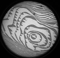
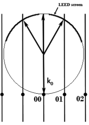
 After a parallel beam of low-energy electrons interacts with a specimen, the electrons form a diffraction or LEED pattern which depends on periodicity present at the surface and is a direct result of the wave nature of an electron. It is important to point out in LEED is that the entire sample surface is being illuminated by a parallel beams of electrons, and thus the diffraction pattern will contain information about the entire surface. The diffraction pattern is formed in the back focal plane of the objective lens, imaged into the object plane of the projective lens (using an intermediate lens), and the final pattern appears on the phosphorescent screen, photographic plate or CCD.
Surface science
Surface science is the study of physical and chemical phenomena that occur at the interface of two phases, including solid–liquid interfaces, solid–gas interfaces, solid–vacuum interfaces, and liquid-gas interfaces. It includes the fields of surface chemistry and surface physics. Some related...
to image atomically clean surfaces, atom-surface interactions, and thin (crystalline) films. In LEEM, high-energy electrons (15-20 keV) are emitted from an electron gun
Electron gun
An electron gun is an electrical component that produces an electron beam that has a precise kinetic energy and is most often used in television sets and computer displays which use cathode ray tube technology, as well as in other instruments, such as electron microscopes and particle...
, focused using a set of condenser optics, and sent through a magnetic beam deflector (usually 60˚ or 90˚). The “fast” electrons travel through an objective lens and begin decelerating to low energies (1-100 eV) near the sample surface because the sample is held at a potential near that of the gun. The low-energy electrons are now termed “surface-sensitive” and the near-surface sampling depth can be varied by tuning the energy of the incident electrons (difference between the sample and gun potentials minus the work functions of the sample and system). The low-energy elastically backscattered electrons travel back through the condenser lens, reaccelerate to the gun voltage (because the condenser lens is grounded), and pass through the beam separator again. However, now the electrons travel away from the condenser optics and into the projector lenses. Imaging of the back focal plane of the objective lens into the object plane of the projector lens (using an intermediate lens) produces a diffraction pattern (low-energy electron diffraction, LEED) at the imaging plane and recorded in a number of different ways. The intensity distribution of the diffraction
Diffraction
Diffraction refers to various phenomena which occur when a wave encounters an obstacle. Italian scientist Francesco Maria Grimaldi coined the word "diffraction" and was the first to record accurate observations of the phenomenon in 1665...
pattern will depend on the periodicity at the sample surface and is a direct result of the wave nature of the electrons. One can produce individual images of the diffraction pattern spot intensities by turning off the intermediate lens and inserting a contrast aperture in the back focal plane of the objective lens (or, in state-of-the-art instruments, in the center of the separator, as chosen by the excitation of the objective lens), thus allowing for real-time observations of dynamic processes at surfaces. Such phenomena include (but are not limited to): tomography, phase transitions, adsorption, reaction, segregation, thin film growth, etching, strain relief, sublimation, and magnetic microstructure. These investigations are only possible because of the accessibility of the sample; allowing for a wide variety of in situ studies over a wide temperature range.
Introduction
- The sample must be illuminated on the same side of the imaging optics, i.e. through the objective lens, because samples are not transparent to low-energy electrons.
- In order to separate the incident and elastically scattered low energy electrons, scientists use magnetic “electron prism” beam separators which focus electrons both in and out of the plane of the beampath (to avoid distortions in the image and diffraction patterns).
- Rather than have the electron gun at a high potential and the rest of the instrument (including electron lenses and specimen) at ground, an electrostatic immersion objective lens brings the sample close to that of the gun, slowing down the high energy electrons to a desired energy only just before interacting with the sample surface.
- The instrument must be able to work under ultra-high vacuum (UHV), or 10−10 torr (760 torr = 1 atm, atmospheric pressure).
Surface Diffraction
Kinematic or elastic backscattering occurs when low energy (1-100 eV) electrons impinge on a clean, well-ordered crystalline specimen. It is assumed that each electron undergoes only one scattering event, and incident electron beam is described as a plane wave with the wavelength:Scientists use inverse space to describe the periodicity of the lattice and the interaction of the plane wave with the sample surface. In inverse (or "k-space") space, the wave vector of the incident and scattered waves are
and , respectively,and constructive interference occurs at the Laue condition:
where (h,k,l) is a set of integers and
is a vector of the reciprocal lattice.
Experimental Setup
1. Electron gun
Electron gun
An electron gun is an electrical component that produces an electron beam that has a precise kinetic energy and is most often used in television sets and computer displays which use cathode ray tube technology, as well as in other instruments, such as electron microscopes and particle...
, used to generate electrons by way of thermionic or field emission from a source tip. In thermionic emission, electrons escape a source tip (usually made of LaB6) by resistive heating and application of an electric field to effectively lower the energy needed for electrons to escape the surface. Once sufficient thermal vibrational energy is attained electrons may overcome this electrostatic energy barrier, allowing them to travel into vacuum and accelerate down the lens column to the gun potential (because the lenses are at ground). In field emission, rather than heating the tip to vibrationally excite electrons from the surface, the source tip (usually tungsten) is sharpened to a small point such that when large electric fields are applied, they concentrate at the tip, lowering the barrier to escape the surface as well as making tunneling of electrons from the tip to vacuum level more feasible.
2. Condenser/illumination optics, used to focus electrons leaving the electron gun and manipulate and/or translate the illumination electron beam. Electromagnetic quadrupole electron lenses are used, the number of which depends on how much resolution and focusing flexibility the designer wishes. However, the ultimate resolution of LEEM is usually determined by that of the objective lens.
3. Illumination beam aperture allows researchers to control the area of the specimen which is illuminated (LEEM’s version of electron microscopy’s “selected area diffraction”, termed microdiffraction) and is located in the beam separator on the illumination side.
4. Magnetic beam separator, needed to resolve the illuminating and imaging beam (while in turn spatially separating the optics for each). There has been much development on the technology of electron beam separators; the early separators introduced distortion in either the image or diffraction plane. However, IBM recently developed a hybrid prism array/nested quadratic field design, focusing the electron beams both in and out of the plane of the beampath, allowing for deflection and transfer of the image and diffraction planes without distortion or energy dispersion.
5. Electrostatic immersion objective lens, used to form a real image of the sample by way of a 2/3-magnification virtual image behind the sample. The uniformity of the electrostatic field between the objective lens and specimen, limited by spherical and chromatic aberrations larger than those of any other lenses, ultimately determines the overall performance of the instrument.
6. Contrast aperture, located in the center on the projector lens side of the beam separator. In most electron microscopies, the contrast aperture is introduced into the back focal plan of the objective lens (where the actual diffraction plane lies). However, this is not true in the LEEM, because dark-field imaging (imaging of nonspecular beams) would not be possible because the aperture has to move laterally and would intercept the incident beam for large shifts. Therefore, researchers adjust the excitation of the objective lens so as to produce an image of the diffraction pattern in the middle of the beam separator and choose the desired spot intensity to image using a contrast aperture inserted there. This aperture allows scientists to image diffraction intensities that may be of particular interest (dark field).
7. Illumination optics are employed to magnify the image or diffraction pattern and project it onto the imaging plate or screen.
8. Imaging plate or screen, used to image the electron intensity so that we can see it. This can be done many different ways including, phosphorescent screens, imaging plates, CCDs, among others.
Low energy electron diffraction (LEED)