
Bead probe technology
Encyclopedia
Printed circuit board
A printed circuit board, or PCB, is used to mechanically support and electrically connect electronic components using conductive pathways, tracks or signal traces etched from copper sheets laminated onto a non-conductive substrate. It is also referred to as printed wiring board or etched wiring...
(PCB) circuitry for performing in-circuit testing (ICT)
In-circuit test
In-circuit test is an example of white box testing where an electrical probe tests a populated printed circuit board , checking for shorts, opens, resistance, capacitance, and other basic quantities which will show whether the assembly was correctly fabricated...
.
Printed circuit board
A printed circuit board, or PCB, is used to mechanically support and electrically connect electronic components using conductive pathways, tracks or signal traces etched from copper sheets laminated onto a non-conductive substrate. It is also referred to as printed wiring board or etched wiring...
(PCB) circuitry for performing in-circuit testing (ICT)
In-circuit test
In-circuit test is an example of white box testing where an electrical probe tests a populated printed circuit board , checking for shorts, opens, resistance, capacitance, and other basic quantities which will show whether the assembly was correctly fabricated...
. http://www.home.agilent.com/agilent/editorial.jspx?action=download&cc=US&lc=eng&ckey=873640&id=873640 http://www.agilent.com/see/beadprobe It makes use of small beads of solder
Solder
Solder is a fusible metal alloy used to join together metal workpieces and having a melting point below that of the workpiece.Soft solder is what is most often thought of when solder or soldering are mentioned and it typically has a melting range of . It is commonly used in electronics and...
placed onto the board's traces to allow measuring and controlling of the signals using a test probe. This permits test access to boards on which standard ICT test pads are not feasible due to space constraints.
Description
Bead probe technology is a probing method used to connect electronic test equipment to the device under testDevice under test
Device under test , also known as unit under test , is a term commonly used to refer to a manufactured product undergoing testing.-In semiconductor testing:...
(DUT) within a bed of nails fixture. The technique was first used in the 1990sSurface Mount & Mixed Technology PCB Design Guidelines by David Boswell. Page 28 ISBN 10 1872422012 and originally given the name “Waygood Bump” after one of the main proponents, Rex Waygood. They are also commonly referred to as solder bumps.Surface Mount Technology – Principles and Practices 2nd Edition by Ray. P Prasad Page 332 ISBN 0-412-12921-3 Bead probes were designed for when less than 30 mil is available for test probe points on the PCB. They are used with standard ICT spring-loaded test probes to connect the test equipment to the DUT.
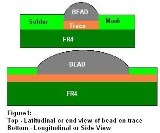
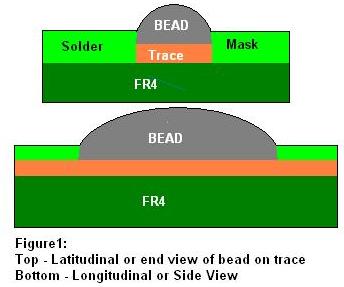
Bead construction
Bead probes are made from a very small "beads" of solder that fit atop of the PCB traces. They are manufactured using the same techniques as other solder features. Construction requires a hole to be opened in the solder maskSolder mask
Solder mask or solder resist is a lacquer-like layer of polymer that provides a permanent protective coating for the copper traces of a printed circuit board and prevents solder from bridging between conductors, thereby preventing short circuits. Solder mask was created primarily to facilitate...
, exposing the copper trace. This hole is sized to precisely control the amount of metal that forms the bead. Solder paste
Solder paste
Solder paste sometimes refers to soldering flux that does not contain solder.Solder paste is used to connect the leads of integrated chip packages to attachment points in the circuit patterns on a printed circuit board...
is applied to the location and reflowed
Reflow soldering
Reflow soldering is a process in which a solder paste is used to temporarily attach one or several electrical components to their contact pads, after which the entire assembly is subjected to controlled heat, which melts the solder, permanently connecting the joint...
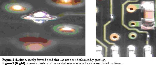
. During reflow, solder flows and is drawn to the copper trace. Surface tension causes the bead to have a curved surface and rise above the solder mask, where it solidifies into a Bead Probe. The bead will be roughly obround in shape and may be 15-25 mils long. A properly constructed bead is the same width as the trace and just enough to clear the surrounding solder mask. The bead is then accessible for testing using a probe with a flat end, which can help compensate for the tolerance build up in the test fixture and PCB.
Advantages
Bead probe can be used in circuits where the pin-pitch is too fine to allow standard test pads. This is becoming more common as pin pitches continue to reduce, particularly in embedded devices. Typically bead probe widths are the width of the PCB traces with a length of about three times this. This allows a high degree of flexibility in their positioning, and can in some cases be applied retrospectively to existing layouts.Because of their small size, bead probes do not affect the signal quality of the signals transferring within the PCB trace. A New Probing Technique for High-Speed/High-Density Printed Circuit Boards by Kenneth P. Parker of Agilent Technologies Applying a New In-Circuit Probing Technique for High-Speed/High Density Printed Circuit Boards to a Real-Life Product by Chris Jacobsen and Kevin Wible of Agilent Technologies This is especially useful in high speed input/output (HSIO) interconnects, where a standard test pad would interfere with the signal.
Disadvantages
- The soldering process that forms the bead probe leaves a coating of fluxFlux (metallurgy)In metallurgy, a flux , is a chemical cleaning agent, flowing agent, or purifying agent. Fluxes may have more than one function at a time...
. Depending on the manufacturing process used, this flux can have varying levels of hardness. Flux with a waxy hardness can reduce the deformation force from the bead, preventing proper contact with the test probe during the first pass contact. This becomes less of an issue on subsequent contacts as the flux is displaced. Test probes with serrated ends of an appropriate size can also aid in measuring bead probes where flux is an issue. - Bead probes require the trace being tested to be located on the surface. This makes it unsuitable for testing high-density boards with many obscured or internal traces and buried viaVia (electronics)A via is a vertical electrical connection between different layers of conductors in a physical electronic circuit.- In IC :In integrated circuit design, a via is a small opening in an insulating oxide layer that allows a conductive connection between different layers. A via on an integrated circuit...
s.
Alternatives
- Boundary scanBoundary scanBoundary scan is a method for testing interconnects on printed circuit boards or sub-blocks inside an integrated circuit. Boundary scan is also widely used as a debugging method to watch integrated circuit pin states, measure voltage, or analyze sub-blocks inside an integrated circuit.The Joint...
integrates test components into the integrated circuitIntegrated circuitAn integrated circuit or monolithic integrated circuit is an electronic circuit manufactured by the patterned diffusion of trace elements into the surface of a thin substrate of semiconductor material...
s (ICs) mounted on the board, giving the ability to read or drive the ICs' pins. This allows for testing of interconnects for which physical access is not an option, such as BGABall grid arrayA ball grid array is a type of surface-mount packaging used for integrated circuits.- Description :The BGA is descended from the pin grid array , which is a package with one face covered with pins in a grid pattern. These pins conduct electrical signals from the integrated circuit to the printed...
components or signal routes sandwiched between plane layers. A boundary scan controller uses four or more dedicated pins on the board to control test cells seriallySerial communicationIn telecommunication and computer science, serial communication is the process of sending data one bit at a time, sequentially, over a communication channel or computer bus. This is in contrast to parallel communication, where several bits are sent as a whole, on a link with several parallel channels...
and receive the measured values. It has the disadvantage of needing board infrastructure to support boundary scan. - Test Access Component (TAC) uses a device such as a 0201Surface-mount technologySurface mount technology is a method for constructing electronic circuits in which the components are mounted directly onto the surface of printed circuit boards . An electronic device so made is called a surface mount device...
as a target for a large probe as in the solder bump examples. The advantage of this technique is that it provides two target points at each end of the package. The disadvantage of this technique is it can add process and cost to the PCB. TEST ACCESS COMPONENT FOR AUTOMATIC TESTING OF CIRCUIT ASSEMBLIES United States Patent Application 20100207651 - A technique has been describedVAUCHER, C., Analog/Digital Testing of Loaded Boards Without Dedicated Test Points, Proceedings of the International Test Conference, IEEE 1996, pp. 325-32. which opens up windows in the solder mask to create test points located directly on PCB tracks. This technique uses a conductive rubber tipped probe to contact the test point which could have a conductive Hot Air Solder Levelling (HASL)HASLHASL or Hot Air Solder Leveling is a type of finish used on printed circuit boards .- Description :The PCB is typically dipped into a bath of molten solder such that all exposed copper surfaces are covered by solder. Excess solder is removed by scraping the PCB with hot air knives.The HASL process...
finish.