
Stencil lithography
Encyclopedia
Stencil lithography is a novel method of fabricating nanometer scale patterns. It is a resist-less, simple, parallel nanolithography
process, and it does not involve any heat or chemical treatment of the substrates (unlike resist
-based techniques).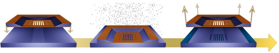
Various materials can be used as membranes, such as metals, Si, SixNy, and polymers. Today the stencil apertures can be scaled down to sub-micrometer size at full 4" wafer scale. This is called a nanostencil
. Nano-scale stencil apertures have been fabricated using laser interference lithography
(LIL), electron beam lithography
, and focused ion beam
lithography.
. This includes thermal and electron beam physical vapor deposition
, molecular beam epitaxy
, sputtering
, and pulsed laser deposition
. The more directional the material flux is, the more accurate the pattern is transferred form the stencil to the substrate.
The accuracy of the pattern transfer from the stencil to the substrate depends on many parameters. The material diffusion on the substrate (as a function of temperature, material type, evaporation angle) and the geometrical setup of the evaporation are the main factors. Both lead to an enlargement of the initial pattern, called blurring.
Nanolithography
Nanolithography is the branch of nanotechnology concerned with the study and application of fabricating nanometer-scale structures, meaning patterns with at least one lateral dimension between the size of an individual atom and approximately 100 nm...
process, and it does not involve any heat or chemical treatment of the substrates (unlike resist
Resist
In semiconductor fabrication, a resist is a thin layer used to transfer a circuit pattern to the semiconductor substrate which it is deposited upon. A resist can be patterned via lithography to form a micrometer-scale, temporary mask that protects selected areas of the underlying substrate during...
-based techniques).
History
Stencil lithography was first reported in a scientific journal as a micro-structuring technique by S. Grey and P. K. Weimer in 1959. They used long stretched metallic wires as shadow masks during metal deposition.Various materials can be used as membranes, such as metals, Si, SixNy, and polymers. Today the stencil apertures can be scaled down to sub-micrometer size at full 4" wafer scale. This is called a nanostencil
Nanostencil
Nanostencil is a stencil with nanometer size apertures. The technique used to pattern materials with nanostencils is called stencil lithography....
. Nano-scale stencil apertures have been fabricated using laser interference lithography
Interference lithography
Interference lithography is a technique for patterning regular arrays of fine features, without the use of complex optical systems or photomasks.-Basic principle:...
(LIL), electron beam lithography
Electron beam lithography
Electron beam lithography is the practice of emitting a beam of electrons in a patterned fashion across a surface covered with a film , and of selectively removing either exposed or non-exposed regions of the resist...
, and focused ion beam
Focused ion beam
Focused ion beam, also known as FIB, is a technique used particularly in the semiconductor industry, materials science and increasingly in the biological field for site-specific analysis, deposition, and ablation of materials. An FIB setup is a scientific instrument that resembles a scanning...
lithography.
Processes
Several process are available using stencil lithography: material deposition and etching, as well as implantation of ions. Different stencil requirements are necessary for the various processes, e. g. an extra etch-resistant layer on the backside of the stencil for etching (if the membrane material is sensitive to the etching process) or a conductive layer on the backside of the stencil for ion implantation.Deposition
The main deposition method used with stencil lithography is physical vapor depositionPhysical vapor deposition
Physical vapor deposition is a variety of vacuum deposition and is a general term used to describe any of a variety of methods to deposit thin films by the condensation of a vaporized form of the desired film material onto various workpiece surfaces...
. This includes thermal and electron beam physical vapor deposition
Electron Beam Physical Vapor Deposition
Electron Beam Physical Vapor Deposition or EBPVD is a form of physical vapor deposition in which a target anode is bombarded with an electron beam given off by a charged tungsten filament under high vacuum. The electron beam causes atoms from the target to transform into the gaseous phase...
, molecular beam epitaxy
Molecular beam epitaxy
Molecular beam epitaxy is one of several methods of depositing single crystals. It was invented in the late 1960s at Bell Telephone Laboratories by J. R. Arthur and Alfred Y. Cho.-Method:...
, sputtering
Sputtering
Sputtering is a process whereby atoms are ejected from a solid target material due to bombardment of the target by energetic particles. It is commonly used for thin-film deposition, etching and analytical techniques .-Physics of sputtering:...
, and pulsed laser deposition
Pulsed laser deposition
Pulsed laser deposition is a thin film deposition technique where a high power pulsed laser beam is focused inside a vacuum chamber to strike a target of the material that is to be deposited...
. The more directional the material flux is, the more accurate the pattern is transferred form the stencil to the substrate.
Etching
Reactive ion etching is based on ionized, accelerated particles that etch both chemically and physically the substrate. The stencil in this case is used as a hard mask, protecting the covered regions of the substrate, while allowing the substrate under the stencil apertures to be etched.Ion implantation
Here the thickness of the membrane has to be smaller than the penetration length of the ions in the membrane material. The ions will then implant only under the stencil apertures, into the substrate.Modes
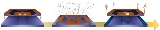
There are three main modes of operation of stencil lithography: static, quasi-dynamic and dynamic. While all the above described processes have been proven using the static mode (stencil doesn't move relative to substate during material or ion processing), only ion implantation has been shown for the non-static modes (quasi-dynamic).Static stencil
In the static mode, the stencil is aligned (if necessary) and fixed to a substrate. The stencil-substrate pair is placed in the evaporation/etching/ion implantation machine, and after the processing is done, the stencil is simply removed from the now patterned substrate.Quasi-dynamic stencil
In the quasi-dynamic mode (or step-and-repeat), the stencil moves relative to the substrate in between depositions, without breaking the vacuum.Dynamic stencil
In the dynamic mode, the stencil moves relative to the substrate during deposition, allowing the fabrication of patterns with tapered height profiles by changing the stencil speed during a contstant material deposition rate.Challenges
Despite it being a versatile technique, there are still several challenges to be addressed by stencil lithography. During deposition through the stencil, material is deposited not only on the substrate through the apertures but also on the stencil backside, including around and inside the apertures. This reduces the effective aperture size by an amount proportional to the deposited material, leading ultimately to aperture clogging.The accuracy of the pattern transfer from the stencil to the substrate depends on many parameters. The material diffusion on the substrate (as a function of temperature, material type, evaporation angle) and the geometrical setup of the evaporation are the main factors. Both lead to an enlargement of the initial pattern, called blurring.
External links
- http://lmis1.epfl.ch/page-34708-en.html
- http://www.microlitho.com/