
Silicon on sapphire
Encyclopedia
Silicon on sapphire is a hetero-epitaxial
process for integrated circuit
manufacturing that consists of a thin layer (typically thinner than 0.6 micrometres) of silicon
grown on a sapphire
(Al2O3) wafer. SOS is part of the Silicon on Insulator
(SOI) family of CMOS
technologies. SOS is primarily used in aerospace
and military
applications because of its inherent resistance to radiation. Typically, high-purity artificially grown sapphire
crystals are used. The silicon is usually deposited by the decomposition of silane gas (SiH4) on heated sapphire substrates. The advantage of sapphire is that it is an excellent electrical insulator
, preventing stray currents caused by radiation from spreading to nearby circuit elements. SOS has seen little commercial use to date because of difficulties in fabricating the very small transistor
s used in modern high-density applications. This drawback is because the SOS process results in the formation of dislocations, twinning and stacking faults from crystal lattice disparities between the sapphire and silicon. Additionally, there is some aluminium
, a p-type dopant
, contamination from the substrate in the silicon closest to the interface.
(23) is commonly referred to as alumina, or corundum
in its crystalline form, as well as many other names, reflecting its widespread occurrence in nature and industry. "Sapphire" usually refers to one of the gem-varieties of corundum (α-alumina), which occur naturally with trace impurities (see ruby
and emery
). In contrast, "sapphire" in the context of SOS refers to high purity alumina wafers grown as a large crystal in a controlled environment. The result is an extremely pure single crystal of alumina that can weigh more than 50 kg. The sapphire wafer is not cut on the crystal axis of symmetry, but instead is cut at an angle of about 60° along what is called the “r-plane”. In crystallographic notation this is the (1-102) plane.
In a remarkable phenomenon of nature, the r-plane of sapphire has oxygen atoms spaced at a distance that is close to the spacing of the atoms in the (100) plane of a silicon crystal. The oxygen atoms on the r-plane have a square symmetry that also mirrors the symmetry of the (100) plane of silicon. The (100) plane of silicon is the same crystal plane that is used in all CMOS electronics. The square symmetry of the r-plane of sapphire is illustrated in Figure 1.
Notice that there is an extra oxygen atom available in each set of four. A silicon atom can bond to one of the corner oxygen atoms in addition to this one to form a simple SiO2 bond. The extra oxygen atom is spaced at approximately the distance between the oxygen atoms in single crystal SiO2. The remarkable compatibility between the (1-102) plane of sapphire and the (100) plane of silicon is what enables SOS technology.
In the mid-1960s researchers at the RCA Laboratories in Princeton, New Jersey worked on making SOS a manufacturable technology. The primary application was for radiation hard circuits, but these researchers also realized the speed and low power benefits of SOS could lead to commercial applications. RCA led the development of SOS technology into the mid-1970s and in fact still processes SOS for space applications.
The first attempt at commercializing SOS was by a company named Inselek, a spin-off of RCA. The early 1970s were a time where the future seemed bright for SOS. In a review article in 1972, Edward Ross of Inselek wrote that, “The principal metallurgical, chemical and electrical properties of SOS films prove to be as good as, or better than, those of chemically or mechanically polished bulk silicon wafers” [3]. Inselek did not survive into the 1980s.
The one notable commercial application of SOS in the late 1970s and into the 1980s was in the Hewlett- Packard 41-Series calculators. SOS was adopted by Hewlett-Packard because of its low power consumption. Soon bulk silicon captured the low power market and has only recently been displaced by SOI.
The technological barrier to SOS becoming commercially successful in the 1970s was the high number of defects in the film. The defects cause leakage current when the transistor is off and reduce carrier mobility. Mobility is a measurement of how fast charge can accelerate in a semiconductor, or indirectly, a transistor’s maximum frequency of operation. It had been known for some years that as the silicon film is grown thicker, the quality of the film improves and the mobility increases. High resolution images of the atomic structure, such as is shown in Figure 2, show how the defects grow together and cancel each other, leading to a higher quality film farther away from the silicon/sapphire interface.
SOS was successfully used in these thicker films where the defect density is reduced, but in order to achieve really high performance, an ultra-thin film is required. An ultra-thin film is generally considered to be less than 100 nm, or only about 100 atoms, thick. Ultra- thin films enable the use of shorter gate lengths, which leads to higher speed electronics.
The breakthrough that enabled ultra-thin SOS films was developed by Silvanus Lau at the California Institute of Technology and researchers at Hewlett-Packard in 1978. The process is called Solid Phase Epitaxial Regrowth (SPER). The first part of SPER is a silicon implant. The implant parameters are set so that the silicon crystal is amorphized in the region near the sapphire interface, but the better quality crystal away from the interface is left intact. An anneal then regrows the amorphous silicon into a single crystal by using the upper layer of the film as a template. The final step is the thinning of the silicon layer to about 100 nm thickness by oxidation. Figure 3 provides a schematic illustration of the SPER process.
The SPER technique was never used commercially by Hewlett-Packard. Work continued on refining this process, however, at the Naval Ocean Systems Center (NOSC) in San Diego, California. It was at NOSC that the RF applications of ultra-thin SOS began to be explored. In 1990, former NOSC researchers Dr. Ron Reedy and Dr. Mark Burgener, along with partner Rory Moore, founded Peregrine Semiconductor
in San Diego, California, commercializing silicon on sapphire for the first time.
Silicon on sapphire benefits from its similarity to bulk silicon by its use of the same basic CMOS technology. The reason that bulk silicon dominates the semiconductor market is not because of raw performance. Certainly, exotic III-V semiconductor technologies (such as GaAs) have better electron mobility and higher breakdown fields than silicon. The key to bulk silicon’s success is in the fundamental benefits of standard CMOS processing; that is: high manufacturing yields, low power operation and high levels of integration. Silicon on sapphire benefits from all the process refinements that have been developed for CMOS on bulk silicon, and from the existing manufacturing infrastructure that was assembled around silicon.
A big advantage of silicon on sapphire over exotic technologies is that it is manufactured in the same factories that produce common bulk silicon wafers. A further advantage is that, because of its better performance, it can be manufactured in a less advanced factory than similar devices in bulk silicon. The performance that is obtained for a given technology in silicon on sapphire is about two generations ahead of the performance of bulk silicon. For example, the 0.25μm technology node in SOS has similar performance to the 0.13μm node in bulk silicon.
Where silicon on sapphire has disadvantages over bulk silicon is that it is by nature a more complex process. Sapphire substrates are expensive. They are physically heavy, causing problems with manufacturing machines not designed for their mass. It is difficult and expensive to make them smooth enough for lithography. Sapphire heats and cools at different rates than silicon. The sapphire/silicon interface sometimes has defect issues. Sapphire is transparent, causing issues with optical inspection machines during processing. Cutting or breaking wafers post fabrication is more difficult due to the hardness of the sapphire substrate. These difficulties represent a small number of the details that must be worked out for a fabricator to process a silicon on sapphire wafer.
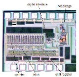
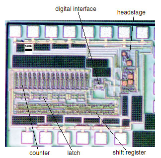 The advantages of the SOS technology allowed research groups as Yale e-Lab to fabricate a variety of SOS circuits and system that benefit from the technology and advance the state-of-the-art in:
Silicon on sapphire pressure and temperature sensors have been manufactured by Sensotron and Sensonetics utilizing a patented process by Armen Sahagen.
A form of silicon on sapphire technology called UltraCMOS was patented by Peregrine Semiconductor, and has been used in commercial mobile handsets as well as rad-hard space applications.
A book on the subject is: "Silicon-on-Sapphire Circuits and Systems, Sensor and Biosensor interfaces" by Eugenio Culurciello published by McGraw Hill in 2009.
Epitaxy
Epitaxy refers to the deposition of a crystalline overlayer on a crystalline substrate, where the overlayer is in registry with the substrate. In other words, there must be one or more preferred orientations of the overlayer with respect to the substrate for this to be termed epitaxial growth. The...
process for integrated circuit
Integrated circuit
An integrated circuit or monolithic integrated circuit is an electronic circuit manufactured by the patterned diffusion of trace elements into the surface of a thin substrate of semiconductor material...
manufacturing that consists of a thin layer (typically thinner than 0.6 micrometres) of silicon
Silicon
Silicon is a chemical element with the symbol Si and atomic number 14. A tetravalent metalloid, it is less reactive than its chemical analog carbon, the nonmetal directly above it in the periodic table, but more reactive than germanium, the metalloid directly below it in the table...
grown on a sapphire
Sapphire
Sapphire is a gemstone variety of the mineral corundum, an aluminium oxide , when it is a color other than red or dark pink; in which case the gem would instead be called a ruby, considered to be a different gemstone. Trace amounts of other elements such as iron, titanium, or chromium can give...
(Al2O3) wafer. SOS is part of the Silicon on Insulator
Silicon on insulator
Silicon on insulator technology refers to the use of a layered silicon-insulator-silicon substrate in place of conventional silicon substrates in semiconductor manufacturing, especially microelectronics, to reduce parasitic device capacitance and thereby improving performance...
(SOI) family of CMOS
CMOS
Complementary metal–oxide–semiconductor is a technology for constructing integrated circuits. CMOS technology is used in microprocessors, microcontrollers, static RAM, and other digital logic circuits...
technologies. SOS is primarily used in aerospace
Aerospace
Aerospace comprises the atmosphere of Earth and surrounding space. Typically the term is used to refer to the industry that researches, designs, manufactures, operates, and maintains vehicles moving through air and space...
and military
Military
A military is an organization authorized by its greater society to use lethal force, usually including use of weapons, in defending its country by combating actual or perceived threats. The military may have additional functions of use to its greater society, such as advancing a political agenda e.g...
applications because of its inherent resistance to radiation. Typically, high-purity artificially grown sapphire
Sapphire
Sapphire is a gemstone variety of the mineral corundum, an aluminium oxide , when it is a color other than red or dark pink; in which case the gem would instead be called a ruby, considered to be a different gemstone. Trace amounts of other elements such as iron, titanium, or chromium can give...
crystals are used. The silicon is usually deposited by the decomposition of silane gas (SiH4) on heated sapphire substrates. The advantage of sapphire is that it is an excellent electrical insulator
Electrical insulation
thumb|250px|[[Coaxial Cable]] with dielectric insulator supporting a central coreThis article refers to electrical insulation. For insulation of heat, see Thermal insulation...
, preventing stray currents caused by radiation from spreading to nearby circuit elements. SOS has seen little commercial use to date because of difficulties in fabricating the very small transistor
Transistor
A transistor is a semiconductor device used to amplify and switch electronic signals and power. It is composed of a semiconductor material with at least three terminals for connection to an external circuit. A voltage or current applied to one pair of the transistor's terminals changes the current...
s used in modern high-density applications. This drawback is because the SOS process results in the formation of dislocations, twinning and stacking faults from crystal lattice disparities between the sapphire and silicon. Additionally, there is some aluminium
Aluminium
Aluminium or aluminum is a silvery white member of the boron group of chemical elements. It has the symbol Al, and its atomic number is 13. It is not soluble in water under normal circumstances....
, a p-type dopant
Dopant
A dopant, also called a doping agent, is a trace impurity element that is inserted into a substance in order to alter the electrical properties or the optical properties of the substance. In the case of crystalline substances, the atoms of the dopant very commonly take the place of elements that...
, contamination from the substrate in the silicon closest to the interface.
Sapphire wafer
Aluminium oxideAluminium oxide
Aluminium oxide is an amphoteric oxide with the chemical formula 23. It is commonly referred to as alumina, or corundum in its crystalline form, as well as many other names, reflecting its widespread occurrence in nature and industry...
(23) is commonly referred to as alumina, or corundum
Corundum
Corundum is a crystalline form of aluminium oxide with traces of iron, titanium and chromium. It is a rock-forming mineral. It is one of the naturally clear transparent materials, but can have different colors when impurities are present. Transparent specimens are used as gems, called ruby if red...
in its crystalline form, as well as many other names, reflecting its widespread occurrence in nature and industry. "Sapphire" usually refers to one of the gem-varieties of corundum (α-alumina), which occur naturally with trace impurities (see ruby
Ruby
A ruby is a pink to blood-red colored gemstone, a variety of the mineral corundum . The red color is caused mainly by the presence of the element chromium. Its name comes from ruber, Latin for red. Other varieties of gem-quality corundum are called sapphires...
and emery
Emery (mineral)
Emery is a very hard rock type used to make abrasive powder. It largely consists of the mineral corundum , mixed with other species such as the iron-bearing spinels hercynite and magnetite, and also rutile...
). In contrast, "sapphire" in the context of SOS refers to high purity alumina wafers grown as a large crystal in a controlled environment. The result is an extremely pure single crystal of alumina that can weigh more than 50 kg. The sapphire wafer is not cut on the crystal axis of symmetry, but instead is cut at an angle of about 60° along what is called the “r-plane”. In crystallographic notation this is the (1-102) plane.
In a remarkable phenomenon of nature, the r-plane of sapphire has oxygen atoms spaced at a distance that is close to the spacing of the atoms in the (100) plane of a silicon crystal. The oxygen atoms on the r-plane have a square symmetry that also mirrors the symmetry of the (100) plane of silicon. The (100) plane of silicon is the same crystal plane that is used in all CMOS electronics. The square symmetry of the r-plane of sapphire is illustrated in Figure 1.
Notice that there is an extra oxygen atom available in each set of four. A silicon atom can bond to one of the corner oxygen atoms in addition to this one to form a simple SiO2 bond. The extra oxygen atom is spaced at approximately the distance between the oxygen atoms in single crystal SiO2. The remarkable compatibility between the (1-102) plane of sapphire and the (100) plane of silicon is what enables SOS technology.
History
SOS was invented in 1963 at North American Aviation (now Boeing), Autonetics Division in Anaheim, California. The first published report is by Harold Manasevit and William Simpson [2]. A very practical experiment led to the discovery of SOS. A sapphire crystal was polished into a spherical shape and immersed in a gas containing silicon. A spherical surface will expose all of the planes that exist in a crystal system. It was found that (100) silicon grew in certain sites on the sphere, and these were identified as corresponding to the (1102) plane of sapphire. Manasevit also deposited silicon films on spinel and cubic zirconia, but these technologies never made it out of the laboratory.In the mid-1960s researchers at the RCA Laboratories in Princeton, New Jersey worked on making SOS a manufacturable technology. The primary application was for radiation hard circuits, but these researchers also realized the speed and low power benefits of SOS could lead to commercial applications. RCA led the development of SOS technology into the mid-1970s and in fact still processes SOS for space applications.
The first attempt at commercializing SOS was by a company named Inselek, a spin-off of RCA. The early 1970s were a time where the future seemed bright for SOS. In a review article in 1972, Edward Ross of Inselek wrote that, “The principal metallurgical, chemical and electrical properties of SOS films prove to be as good as, or better than, those of chemically or mechanically polished bulk silicon wafers” [3]. Inselek did not survive into the 1980s.
The one notable commercial application of SOS in the late 1970s and into the 1980s was in the Hewlett- Packard 41-Series calculators. SOS was adopted by Hewlett-Packard because of its low power consumption. Soon bulk silicon captured the low power market and has only recently been displaced by SOI.
The technological barrier to SOS becoming commercially successful in the 1970s was the high number of defects in the film. The defects cause leakage current when the transistor is off and reduce carrier mobility. Mobility is a measurement of how fast charge can accelerate in a semiconductor, or indirectly, a transistor’s maximum frequency of operation. It had been known for some years that as the silicon film is grown thicker, the quality of the film improves and the mobility increases. High resolution images of the atomic structure, such as is shown in Figure 2, show how the defects grow together and cancel each other, leading to a higher quality film farther away from the silicon/sapphire interface.
SOS was successfully used in these thicker films where the defect density is reduced, but in order to achieve really high performance, an ultra-thin film is required. An ultra-thin film is generally considered to be less than 100 nm, or only about 100 atoms, thick. Ultra- thin films enable the use of shorter gate lengths, which leads to higher speed electronics.
Ultra-thin silicon film
Another advantage of ultra-thin films is that so-called “fully depleted” transistors may be used. Without going into detailed semiconductor physics, “fully depleted” simply means that the conducting channel of the transistor is depleted of charge by the time the transistor turns on. This can only occur in SOI technologies because in bulk silicon there is an almost infinite source of charge available that can not be depleted. The performance advantage of fully depleted transistors comes from the fact that when there is no charge in the channel, the entire gate voltage is applied to create a conducting channel. This essentially acts like a thinner gate oxide, increasing the drive current of the transistor.The breakthrough that enabled ultra-thin SOS films was developed by Silvanus Lau at the California Institute of Technology and researchers at Hewlett-Packard in 1978. The process is called Solid Phase Epitaxial Regrowth (SPER). The first part of SPER is a silicon implant. The implant parameters are set so that the silicon crystal is amorphized in the region near the sapphire interface, but the better quality crystal away from the interface is left intact. An anneal then regrows the amorphous silicon into a single crystal by using the upper layer of the film as a template. The final step is the thinning of the silicon layer to about 100 nm thickness by oxidation. Figure 3 provides a schematic illustration of the SPER process.
The SPER technique was never used commercially by Hewlett-Packard. Work continued on refining this process, however, at the Naval Ocean Systems Center (NOSC) in San Diego, California. It was at NOSC that the RF applications of ultra-thin SOS began to be explored. In 1990, former NOSC researchers Dr. Ron Reedy and Dr. Mark Burgener, along with partner Rory Moore, founded Peregrine Semiconductor
Peregrine Semiconductor
Peregrine Semiconductor is a San Diego-based manufacturer of high-performance RF CMOS integrated circuits. The company's UltraCMOS™ process technology is a proprietary implementation of SOS substrates that enables high levels of monolithic integration...
in San Diego, California, commercializing silicon on sapphire for the first time.
Advantages and disadvantages
The most important advantage of silicon on sapphire over bulk silicon technology is its insulating substrate. The insulating substrate virtually eliminates the parasitic drain capacitance that is present in bulk silicon. This does several important things. The simple thing is that it leads to dramatic improvement in transistor performance because this capacitor does not need to be charged and discharged on every cycle. The insulating substrate also provides better isolation between circuit elements. More subtly, because the drain capacitor in bulk silicon is a depletion capacitance between two semiconductor layers it behaves in a non-linear manner. Eliminating this non-linearity enables silicon on sapphire to have significantly better harmonic performance than bulk silicon. In fact, one of the most important performance advantages of III-V semiconductor compounds is their semi-insulating substrates.Silicon on sapphire benefits from its similarity to bulk silicon by its use of the same basic CMOS technology. The reason that bulk silicon dominates the semiconductor market is not because of raw performance. Certainly, exotic III-V semiconductor technologies (such as GaAs) have better electron mobility and higher breakdown fields than silicon. The key to bulk silicon’s success is in the fundamental benefits of standard CMOS processing; that is: high manufacturing yields, low power operation and high levels of integration. Silicon on sapphire benefits from all the process refinements that have been developed for CMOS on bulk silicon, and from the existing manufacturing infrastructure that was assembled around silicon.
A big advantage of silicon on sapphire over exotic technologies is that it is manufactured in the same factories that produce common bulk silicon wafers. A further advantage is that, because of its better performance, it can be manufactured in a less advanced factory than similar devices in bulk silicon. The performance that is obtained for a given technology in silicon on sapphire is about two generations ahead of the performance of bulk silicon. For example, the 0.25μm technology node in SOS has similar performance to the 0.13μm node in bulk silicon.
Where silicon on sapphire has disadvantages over bulk silicon is that it is by nature a more complex process. Sapphire substrates are expensive. They are physically heavy, causing problems with manufacturing machines not designed for their mass. It is difficult and expensive to make them smooth enough for lithography. Sapphire heats and cools at different rates than silicon. The sapphire/silicon interface sometimes has defect issues. Sapphire is transparent, causing issues with optical inspection machines during processing. Cutting or breaking wafers post fabrication is more difficult due to the hardness of the sapphire substrate. These difficulties represent a small number of the details that must be worked out for a fabricator to process a silicon on sapphire wafer.
Circuits and systems
- analog-to-digital converters (a nano-Watts prototype was produced by Yale e-Lab)
- monolithic digital isolation buffers
- SOS-CMOS image sensor arrays (one of the first standard CMOS image sensor arrays capable of transducing light simultaneously from both sides of the die was produced by Yale e-Lab)
- patch-clamp amplifiers
- energy harvesting devices
- three-dimensional (3D) integration with no galvanic connections
- charge pumps
- temperature sensors
- digitally tunable capacitorCapacitorA capacitor is a passive two-terminal electrical component used to store energy in an electric field. The forms of practical capacitors vary widely, but all contain at least two electrical conductors separated by a dielectric ; for example, one common construction consists of metal foils separated...
s
Silicon on sapphire pressure and temperature sensors have been manufactured by Sensotron and Sensonetics utilizing a patented process by Armen Sahagen.
A form of silicon on sapphire technology called UltraCMOS was patented by Peregrine Semiconductor, and has been used in commercial mobile handsets as well as rad-hard space applications.
A book on the subject is: "Silicon-on-Sapphire Circuits and Systems, Sensor and Biosensor interfaces" by Eugenio Culurciello published by McGraw Hill in 2009.