

Scanning joule expansion microscopy
Encyclopedia
Scanning Joule Expansion Microscopy is a form of scanning probe microscopy
heavily based on atomic force microscopy that maps the temperature distribution along a surface. Resolutions down to 10 nm have been achieved and 1 nm resolution is theoretically possible. Thermal measurements at the nanometer scale are of both academic and industrial interest, particularly in regards to nanomaterials
and modern integrated circuits.
The deflection signals are caused not only by sample topography, but also by the thermal expansion caused by Joule heating. Since AFM has feedback controller with a bandwidth, for example 20 kHz (different AFM may have different bandwidths), the signal below 20 kHz is captured and processed by the feedback controller which then adjusts the z-piezo to image surface topography. Joule heating frequency is kept well above 20 kHz to avoid feedback response and to separate topological and thermal effects. The upper limit of the frequency is limited by the decrease of thermoelastic expansion with the inverse power of the modulation frequency and the frequency characteristics of the cantilever arrangement. A lock-in amplifier is specially tuned to the Joule heating frequency for detecting only the expansion signal and provides the information to an auxiliary Atomic Force Microscopy channel to create the thermal expansion image. Usually expansion signals approximately 0.1 Angstroms start to be detected, although the resolution of SJEM highly depends on the whole system (cantilever, sample surface, etc).
By comparison, Scanning Thermal Microscopy (SThM) has coaxial thermocouple at the end of sharp metal tip. The spatial resolution of SThM critically depends on the thermocouple sensor size. Much effort has been dedicated to reducing sensor size to sub-micrometre scales. The quality and resolution of the images are very dependent on the nature of the thermal contact between tip and the sample; hence it is quite difficult to control in a reproducible way. The fabrication also becomes very challenging particularly for thermocouple sensor size below 500 nm. With optimization on the design and the fabrication, it was possible to achieve resolution around 25 nm. Scanning Joule Expansion Microscopy, however, has the potential of achieving similar to AFM resolution of 1~10 nm. In practice, however, the spatial resolution is limited to the size of the liquid film bridge between the tip and the sample, which is typically about 20 nm. The microfabricated thermocouples used for Scanning Thermal Microscopy are rather expensive and more importantly very fragile. Scanning Joule Expansion Microscopy has been used to measure the local heat dissipation of an in-plane gate (IPG) transistor to study hot spots in semiconductor devices, and thin-film alloy like cobalt-nickel silicide.
 , in which C is the tip sample capacitance, and V is the voltage, Z is the tip and sample distance. Interestingly, this force also depends on
  , the same as the expansion signal. Usually electrostatic force is small because the sample has been covered with a polymer layer. However, when applied voltage is large, this force needs to be considered. Electrostatic force does not depend on the frequency of the applied AC signal, therefore allowing for a simple method to differentiate and account for this contribution.
 ,and applying the known expansion coefficient,
  and polymer thickness, L(which could be measured by AFM or ellipsometer), the expansion signal is obtained. The smallest expansion that can be resolved is about 10pm.
In order to extract accurate temperatures, additional modeling taking into account thermal expansion and cantilever bending is necessary. Moreover, calibration using a reference system, such as metallic films, is required.
The basic thermal equation is:
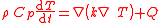
Here, ρCp is the heat capacitance;K is the thermal conductivity and Q is the input power.
Rearrange the equation in a discrete form according to each element:

Here, represents the specific temperature of position element n at time element t. Using software could solve the equations and obtained the temperature T.
The expansion magitude could be obtained by:


is the thermal expansion coefficient of the polymer and L is its thickness.
In addition, size effects also play an important role in modern interconnects. As dimensions of the metal decrease, thermal conductivity begins to decrease from that of the bulk material, further creating cause for concern. SJEM has been used to extract thermal conductivities of constrictions in different thicknesses of thin metallic films. The extracted values show agreement with those predicted by the Wiedemann-Franz law.
Possible materials and devices for thermal mapping include high electron mobility transistors, nanotubes, nanowires, graphene sheets, nanomeshes, and nanoribbons, and other molecular electronic materials. In particular, SJEM can be directly used for characterization of band gap distributions in nanotube transistors, nanowires, and graphene nanomeshes and nanoribbons. It can also be used to locate hotspots and defects in these materials. Another example of a simple, direct application is thermal mapping of rough nanowires for thermolelectric applications.
This technique is far more complex than traditional AFM. Unlike AFM, SJEM needs to consider the type of polymer, the thickness of polymer used to coat the sample and the frequency to drive the device. This additional processing often can degrade or compromise the integrity of the sample. For micro/nano devices, wire-bonding is usually necessary to apply voltage, further increasing processing and decreasing throughput. During scanning, the magnitude of the voltage, frequency, and scanning speeds need to be considered. Calibration must also be done using a reference system in order to ensure accuracy. Finally, a complex model must be used to account for all these factors and parameters.
Second, there may be artifact effects near the edges (or steps). Near the edges where large height differences or material mismatches exist, artifact expansion signals are usually detected. The exact cause has not been found. It is widely believed that the tip sample interaction near the edges can account for these artifacts. At the edges, forces are present not only in the vertical direction but possibly also in the lateral direction, disrupting the cantilever motion. In addition, at a large step, loss of contact between the tip and the sample could result in an artifact in the image. Another concern is that the polymer coating near the step may not be uniform, or possibly not continuous. Further investigations near edges and junctions need to be carried out.
Finally, interactions between the tip and electric field can occur when large gate biases are applied to the substrate. Fringing effects and other geometric concerns can lead to electric field concentrations, leading to large deviations from the normal baseline tip interaction which cannot be easily subtracted. This is especially problematic where the polymer expansion is small, leading to artifacts from this effect dominating. The contribution from these artifacts can be reduced by applying thicker polymer coatings or operating at a lower gate bias to decrease electric field. However, this occurs at the expense of resolution due to increased thermal diffusion in the thicker polymer layer as well as increased noise. In addition, devices may not be fully modulated at lower gate biases.
Scanning probe microscopy
Scanning Probe Microscopy is a branch of microscopy that forms images of surfaces using a physical probe that scans the specimen. An image of the surface is obtained by mechanically moving the probe in a raster scan of the specimen, line by line, and recording the probe-surface interaction as a...
heavily based on atomic force microscopy that maps the temperature distribution along a surface. Resolutions down to 10 nm have been achieved and 1 nm resolution is theoretically possible. Thermal measurements at the nanometer scale are of both academic and industrial interest, particularly in regards to nanomaterials
Nanomaterials
Nanomaterials is a field that takes a materials science-based approach to nanotechnology. It studies materials with morphological features on the nanoscale, and especially those that have special properties stemming from their nanoscale dimensions...
and modern integrated circuits.
Basic Principles
Scanning Joule Expansion Microscopy (SJEM) is based on the contact operation model of Atomic Force Microscopy (AFM). During the operation, the tip on the cantilever is brought into contact with the surface of the sample. AC or pulsed electrical signal is applied to the sample creating Joule heating and resulting in periodic thermal expansion. At the same time, the laser, which is focused on the top surface of the cantilever and the photodiode of the equipment, detects the displacement of the cantilever. The detecting photodiode is composed of two segments, which normalizes the incoming signal deflected from the cantilever. This differential signal is proportional to the cantilever deflection.The deflection signals are caused not only by sample topography, but also by the thermal expansion caused by Joule heating. Since AFM has feedback controller with a bandwidth, for example 20 kHz (different AFM may have different bandwidths), the signal below 20 kHz is captured and processed by the feedback controller which then adjusts the z-piezo to image surface topography. Joule heating frequency is kept well above 20 kHz to avoid feedback response and to separate topological and thermal effects. The upper limit of the frequency is limited by the decrease of thermoelastic expansion with the inverse power of the modulation frequency and the frequency characteristics of the cantilever arrangement. A lock-in amplifier is specially tuned to the Joule heating frequency for detecting only the expansion signal and provides the information to an auxiliary Atomic Force Microscopy channel to create the thermal expansion image. Usually expansion signals approximately 0.1 Angstroms start to be detected, although the resolution of SJEM highly depends on the whole system (cantilever, sample surface, etc).
By comparison, Scanning Thermal Microscopy (SThM) has coaxial thermocouple at the end of sharp metal tip. The spatial resolution of SThM critically depends on the thermocouple sensor size. Much effort has been dedicated to reducing sensor size to sub-micrometre scales. The quality and resolution of the images are very dependent on the nature of the thermal contact between tip and the sample; hence it is quite difficult to control in a reproducible way. The fabrication also becomes very challenging particularly for thermocouple sensor size below 500 nm. With optimization on the design and the fabrication, it was possible to achieve resolution around 25 nm. Scanning Joule Expansion Microscopy, however, has the potential of achieving similar to AFM resolution of 1~10 nm. In practice, however, the spatial resolution is limited to the size of the liquid film bridge between the tip and the sample, which is typically about 20 nm. The microfabricated thermocouples used for Scanning Thermal Microscopy are rather expensive and more importantly very fragile. Scanning Joule Expansion Microscopy has been used to measure the local heat dissipation of an in-plane gate (IPG) transistor to study hot spots in semiconductor devices, and thin-film alloy like cobalt-nickel silicide.
Signal acquisition and analysis
Signal obtained by the AFM (and captured by lock-in amplifier) are actually representations of the cantilever deflection at a specific frequency. However, besides thermal expansion, several other sources may also result in cantilever deflection.Thermally induced cantilever bending
This is usually due to the mismatch in thermal expansion of two cantilever materials, for instance, silicon cantilever coated with a thin layer of metal (to increase the deflection). When heated, materials with higher expansion coefficient will expand more than the material with lower expansion coefficient. In this case, two materials, one in tensile strain, the other in compression strain, will induce substantial bending. However, this mechanism can be excluded for two reasons; first, cantilever coatings have been stripped experimentally and no change in signal was observed; second, the calculated thermal diffusion length in SiNx and Si cantilevers at the SJEM working frequency (typically 10 kHz~100 kHz) is small, much smaller than the length of the cantilever(typically 100 um).Pressure waves
When the sample heats and contracts due to rapid Joule heating from an applied AC power source, pressure waves may be radiated from the sample. This wave may interact with the cantilever, causing additional deflection. However, this possibility is unlikely. For sinusoidal heating, the wavelength of the acoustic wave in air with speed of 340 m/s is about several millimeters, which is much larger than the length of cantilever. Furthermore, experiments have been carried out under vacuum, in which case there are no air pressure waves. In the experiment, it was observed that when the cantilever was out of contact with sample surface, no deflection signal was detected.Piezoelectric effect
In piezoelectric materials, mechanical expansion occurs due to applied bias. Therefore, if the sample is such a material, an additional piezoelectric effect must be considered when analyzing the signal. Typically, piezoelectric expansion is linearly dependent on applied voltage and a simple subtraction can be used to correct for this effect.Electrostatic force interaction
When a bias is applied to the sample for Joule heating, there is also an electrostatic force interaction between the tip and the sample. The tip-sample electrostatic force can be represented as , in which C is the tip sample capacitance, and V is the voltage, Z is the tip and sample distance. Interestingly, this force also depends on , the same as the expansion signal. Usually electrostatic force is small because the sample has been covered with a polymer layer. However, when applied voltage is large, this force needs to be considered. Electrostatic force does not depend on the frequency of the applied AC signal, therefore allowing for a simple method to differentiate and account for this contribution.Thermal expansion
This is primary mode of signal and the main goal of SJEM. The substrate expands when Joule heated, resulting in change in the measured profile by the cantilever, resulting in a change in signal. However, thermal expansion coefficients can vary significantly. For example, the thermal expansion coefficients of metal are typically one order of magnitude higher than those of dielectric and amorphous materials; while the expansion coefficient of polymer is one order higher than those of metals. So by coating the sample surface with a layer of polymer, the expansion signal could be enhanced. More importantly, after coating, the signal only depends on the temperature, independent of the expansion coefficient of different materials, allowing for SJEM to be used for a wide array of samples. Expansion signal increases linearly with temperature and thus quadratically with voltage. In addition, expansion signal increases monotonically with the thickness of coating polymer, while the resolution will decrease due to greater thermal diffusion. Lastly, expansion signal decreases as the frequency increases.Extraction of Temperature
By using the expansion signal, the temperature can be extracted as follows: the signal that captured by the lock-in amplifier is converted into the bending of cantilever. Using,and applying the known expansion coefficient, and polymer thickness, L(which could be measured by AFM or ellipsometer), the expansion signal is obtained. The smallest expansion that can be resolved is about 10pm.In order to extract accurate temperatures, additional modeling taking into account thermal expansion and cantilever bending is necessary. Moreover, calibration using a reference system, such as metallic films, is required.
One dimensional transient finite element model
When the sample is large enough, edge effects can be ignored. Therefore, a simple one dimensional finite element model can be a good approximation.The basic thermal equation is:
Here, ρCp is the heat capacitance;K is the thermal conductivity and Q is the input power.
Rearrange the equation in a discrete form according to each element:
Here,
represents the specific temperature of position element n at time element t. Using software could solve the equations and obtained the temperature T.The expansion magitude could be obtained by:
is the thermal expansion coefficient of the polymer and L is its thickness.
Two or three dimensional finite element model with electrical-thermal-mechanical coupling
Commercialized software can be used for 2D/3D finite element modeling. In such software, the appropriate differential equations for electrical, thermal and mechanical expansion are chosen and proper boundary conditions are set. In addition, electrical-thermal coupling exists in the sample because the resistance is a function of temperature. This is additionally accounted for by typical FEM software packages.Integrated circuit interconnects
Miniaturization of modern integrated circuits has led to hugely increased current densities and therefore, self-heating. In particular, vias, or vertical interconnects, experience extreme local temperature fluctuations, which can strongly influence the electrical performance of multi-level interconnect structures. In addition, these large, highly-localized temperature fluctuations cause repeated stress gradients on the vias, ultimately leading to device failure. Traditional thermometry techniques use electrical characterization to determine resistivity and estimate the average temperature along an interconnect. However, this method is not able to characterize local temperature rises which may be significantly higher near vias due to their extremely high aspect ratios. Optical methods are diffraction limited to resolutions greater than 1 um, far larger than most modern vias feature sizes. SJEM has been used to do in situ thermal mapping of these devices with lateral resolution in the sub-0.1 um range.In addition, size effects also play an important role in modern interconnects. As dimensions of the metal decrease, thermal conductivity begins to decrease from that of the bulk material, further creating cause for concern. SJEM has been used to extract thermal conductivities of constrictions in different thicknesses of thin metallic films. The extracted values show agreement with those predicted by the Wiedemann-Franz law.
Integrated circuit transistors
Understanding thermal properties of transistors are vital for the semiconductor industry as well. Similar to interconnects, repeated thermal stresses can eventually lead to device failure. However, more importantly, electrical behavior, and therefore device parameters change significantly with temperature. SJEM has been used to map local hotspots in thin film transistors. By determining the location of these hotspots, they can be better understood and reduced or eliminated. One disadvantage to this method is that, like AFM, only the surface can be mapped. Consequently, additional processing steps would be required in order to map buried features, such as most features in modern IC transistors.Nanoscale materials
Nanoscale materials are becoming widely investigated for their many advantages in commercial electronics. In particular, these materials are known for excellent mobility as well as ability to carry high current densities. In addition, new applications have been realized for these materials including thermoelectrics, solar cells, fuel cells, etc. However, significant decrease in size scale in conjunction with increases in current density and device density leads to extreme temperature rises in these devices. These temperature fluctuations can influence electrical behavior and lead to device failure. Therefore, these thermal effects must be studied carefully, in situ, to realize nanoscale electronics. SJEM can be used for this purpose, allowing for in situ high-resolution thermal mapping.Possible materials and devices for thermal mapping include high electron mobility transistors, nanotubes, nanowires, graphene sheets, nanomeshes, and nanoribbons, and other molecular electronic materials. In particular, SJEM can be directly used for characterization of band gap distributions in nanotube transistors, nanowires, and graphene nanomeshes and nanoribbons. It can also be used to locate hotspots and defects in these materials. Another example of a simple, direct application is thermal mapping of rough nanowires for thermolelectric applications.
Remaining Questions
Although SJEM is a very powerful technique for temperature detection, significant questions still remain regarding its performance.This technique is far more complex than traditional AFM. Unlike AFM, SJEM needs to consider the type of polymer, the thickness of polymer used to coat the sample and the frequency to drive the device. This additional processing often can degrade or compromise the integrity of the sample. For micro/nano devices, wire-bonding is usually necessary to apply voltage, further increasing processing and decreasing throughput. During scanning, the magnitude of the voltage, frequency, and scanning speeds need to be considered. Calibration must also be done using a reference system in order to ensure accuracy. Finally, a complex model must be used to account for all these factors and parameters.
Second, there may be artifact effects near the edges (or steps). Near the edges where large height differences or material mismatches exist, artifact expansion signals are usually detected. The exact cause has not been found. It is widely believed that the tip sample interaction near the edges can account for these artifacts. At the edges, forces are present not only in the vertical direction but possibly also in the lateral direction, disrupting the cantilever motion. In addition, at a large step, loss of contact between the tip and the sample could result in an artifact in the image. Another concern is that the polymer coating near the step may not be uniform, or possibly not continuous. Further investigations near edges and junctions need to be carried out.
Finally, interactions between the tip and electric field can occur when large gate biases are applied to the substrate. Fringing effects and other geometric concerns can lead to electric field concentrations, leading to large deviations from the normal baseline tip interaction which cannot be easily subtracted. This is especially problematic where the polymer expansion is small, leading to artifacts from this effect dominating. The contribution from these artifacts can be reduced by applying thicker polymer coatings or operating at a lower gate bias to decrease electric field. However, this occurs at the expense of resolution due to increased thermal diffusion in the thicker polymer layer as well as increased noise. In addition, devices may not be fully modulated at lower gate biases.