

Integrating ADC
Encyclopedia
An integrating ADC is a type of analog-to-digital converter
that converts an unknown input voltage into a digital representation through the use of an integrator. In its most basic implementation, the unknown input voltage is applied to the input of the integrator and allowed to ramp for a fixed time period (the run-up period). Then a known reference voltage of opposite polarity is applied to the integrator and is allowed to ramp until the integrator output returns to zero (the run-down period). The input voltage is computed as a function of the reference voltage, the constant run-up time period, and the measured run-down time period. The run-down time measurement is usually made in units of the converter's clock, so longer integration times allow for higher resolutions. Likewise, the speed of the converter can be improved by sacrificing resolution.
Converters of this type can achieve high resolution, but often do so at the expense of speed. For this reason, these converters are not found in audio or signal processing applications. Their use is typically limited to digital voltmeters and other instruments requiring highly accurate measurements.
The conversion takes place in two phases: the run-up phase, where the input to the integrator is the voltage to be measured, and the run-down phase, where the input to the integrator is a known reference voltage. During the run-up phase, the switch selects the measured voltage as the input to the integrator. The integrator is allowed to ramp for a fixed period of time to allow a charge to build on the integrator capacitor. During the run-down phase, the switch selects the reference voltage as the input to the integrator. The time that it takes for the integrator's output to return to zero is measured during this phase.
In order for the reference voltage to ramp the integrator voltage down, the reference voltage needs to have a polarity opposite to that of the input voltage. In most cases, for positive input voltages, this means that the reference voltage will be negative. To handle both positive and negative input voltages, a positive and negative reference voltage is required. The selection of which reference to use during the run-down phase would be based on the polarity of the integrator output at the end of the run-up phase. That is, if the integrator's output were negative at the end of the run-up phase, a negative reference voltage would be required. If the integrator's output were positive, a positive reference voltage would be required.
The basic equation for the output of the integrator (assuming a constant input) is:

Assuming that the initial integrator voltage at the start of each conversion is zero and that the integrator voltage at the end of the run down period will be zero, we have the following two equations that cover the integrator's output during the two phases of the conversion:


The two equations can be combined and solved for , the unknown input voltage:

From the equation, one of the benefits of the dual-slope integrating ADC becomes apparent: the measurement is independent of the values of the circuit elements (R and C). This does not mean, however, that the values of R and C are unimportant in the design of a dual-slope integrating ADC (as will be explained below).
Note that in the graph to the right, the voltage is shown as going up during the run-up phase and down during the run-down phase. In reality, because the integrator uses the op-amp in a negative feedback configuration, applying a positive will cause the output of the integrator to go down. The up and down more accurately refer to the process of adding charge to the integrator capacitor during the run-up phase and removing charge during the run-down phase.
The resolution of the dual-slope integrating ADC is determined primarily by the length of the run-down period and by the time measurement resolution (i.e., the frequency of the controller's clock). The required resolution (in number of bits) dictates the minimum length of the run-down period for a full-scale input ( ):
):

During the measurement of a full-scale input, the slope of the integrator's output will be the same during the run-up and run-down phases. This also implies that the time of the run-up period and run-down period will be equal ( ) and that the total measurement time will be
  . Therefore, the total measurement time for a full-scale input will be based on the desired resolution and the frequency of the controller's clock:

If a resolution of 16 bits is required with a controller clock of 10 MHz, the measurement time will be 13.1 milliseconds (or a sampling rate of just 76 samples per second). However, the sampling time can be improved by sacrificing resolution. If the resolution requirement is reduced to 10 bits, the measurement time is also reduced to only 0.2 milliseconds (almost 4900 samples per second).
A simple way to reduce the run-up time is to increase the rate that charge accumulates on the integrator capacitor by reducing the size of the resistor used on the input, a method referred to as enhanced dual-slope. This still allows the same total amount of charge accumulation, but it does so over a smaller period of time. Using the same algorithm for the run-down phase results in the following equation for the calculation of the unknown input voltage ( ):
):

Note that this equation, unlike the equation for the basic dual-slope converter, has a dependence on the values of the integrator resistors. Or, more importantly, it has a dependence on the ratio of the two resistance values. This modification does nothing to improve the resolution of the converter (since it doesn't address either of the resolution limitations noted above).
One method to increase the integrator capacity is by periodically adding or subtracting known quantities of charge during the run-up phase in order to keep the integrator's output within the range of the integrator amplifier. Then, the total amount of artificially-accumulated charge is the charge introduced by the unknown input voltage plus the sum of the known charges that were added or subtracted.
The circuit diagram shown to the right is an example of how multi-slope run-up could be implemented. The concept is that the unknown input voltage, , is always applied to the integrator. Positive and negative reference voltages controlled by the two independent switches add and subtract charge as needed to keep the output of the integrator within its limits. The reference resistors,
  and
and  are necessarily smaller than
  to ensure that the references can overcome the charge introduced by the input. A comparator
is connected to the output to compare the integrator's voltage with a threshold voltage. The output of the comparator is used by the converter's controller to decide which reference voltage should be applied. This can be a relatively simple algorithm: if the integrator's output above the threshold, enable the positive reference (to cause the output to go down); if the integrator's output is below the threshold, enable the negative reference (to cause the output to go up). The controller keeps track of how often each switch is turned on in order to estimate how much additional charge was placed onto (or removed from) the integrator capacitor as a result of the reference voltages.
To the right is a graph of sample output from the integrator during a multi-slope run-up. Each dashed vertical line represents a decision point by the controller where it samples the polarity of the output and chooses to apply either the positive or negative reference voltage to the input. Ideally, the output voltage of the integrator at the end of the run-up period can be represented by the following equation:

where is the sampling period,
  is the number of periods in which the positive reference is switched in,
  is the number of periods in which the negative reference is switched in, and
  is the total number of periods in the run-up phase.
The resolution obtained during the run-up period can be determined by making the assumption that the integrator output at the end of the run-up phase is zero. This allows us to relate the unknown input, , to just the references and the
  values:

The resolution can be expressed in terms of the difference between single steps of the converter's output. In this case, if we solve the above equation for using
using  and
and 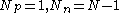 (the sum of
  and
and  must always equal
  ), the difference will equal the smallest resolvable quantity. This results in an equation for the resolution of the multi-slope run-up phase (in bits) of:

Using typical values of the reference resistors and
and  of 10k ohms and an input resistor of 50k ohms, we can achieve a 16 bit resolution during the run-up phase with 655360 periods (65.5 milliseconds with a 10 MHz clock).
While it is possible to continue the multi-slope run-up indefinitely, it is not possible to increase the resolution of the converter to arbitrarily high levels just by using a longer run-up time. Error is introduced into the multi-slope run-up through the action of the switches controlling the references, cross-coupling between the switches, unintended switch charge injection, mismatches in the references, and timing errors.
Some of this error can be reduced by careful operation of the switches. In particular, during the run-up period, each switch should be activated a constant number of times. The algorithm explained above does not do this and just toggles switches as needed to keep the integrator output within the limits. Activating each switch a constant number of times makes the error related to switching approximately constant. Any output offset that is a result of the switching error can be measured and then subtracted from the result.
The circuit shown to the right is an example of a multi-slope run-down circuit with four run-down slopes with each being ten times more gradual than the previous. The switches control which slope is selected. The switch containing selects the steepest slope (i.e., will cause the integrator output to move toward zero the fastest). At the start of the run-down interval, the unknown input is removed from the circuit by opening the switch connected to
  and closing the
  switch. Once the integrator's output reaches zero (and the run-down time measured), the
  switch is opened and the next slope is selected by closing the
  switch. This repeats until the final slope of
  has reached zero. The combination of the run-down times for each of the slopes determines the value of the unknown input. In essence, each slope adds one digit of resolution to the result.
In the example circuit, the slope resistors differ by a factor of 10. This value, known as the base ( ), can be any value. As explained below, the choice of the base affects the speed of the converter and determines the number of slopes needed to achieve the desired resolution.
The basis of this design is the assumption that there will always be overshoot when trying to find the zero crossing at the end of a run-down interval. This will necessarily be true given any hysteresis in the output of the comparator measuring the zero crossing and due to the periodic sampling of the comparator based on the converter's clock. If we assume that the converter switches from one slope to the next in a single clock cycle (which may or may not be possible), the maximum amount of overshoot for a given slope would be the largest integrator output change in one clock period:

To overcome this overshoot, the next slope would require no more than clock cycles, which helps to place a bound on the total time of the run-down. The time for the first-run down (using the steepest slope) is dependent on the unknown input (i.e., the amount of charge placed on the integrator capacitor during the run-up phase). At most, this will be:

where is the maximum number of clock periods for the first slope,
  is the maximum integrator voltage at the start of the run-down phase, and
  is the resistor used for the first slope.
The remainder of the slopes have a limited duration based on the selected base, so the remaining time of the conversion (in converter clock periods) is:

where is the number of slopes.
Converting the measured time intervals during the multi-slope run-down into a measured voltage is similar to the charge-balancing method used in the multi-slope run-up enhancement. Each slope adds or subtracts known amounts of charge to/from the integrator capacitor. The run-up will have added some unknown amount of charge to the integrator. Then, during the run-down, the first slope subtracts a large amount of charge, the second slope adds a smaller amount of charge, etc. with each subsequent slope moving a smaller amount in the opposite direction of the previous slope with the goal of reaching closer and closer to zero. Each slope adds or subtracts a quantity of charge proportional to the slope's resistor and the duration of the slope:

 is necessarily an integer and will be less than or equal to
  for the second and subsequent slopes. Using the circuit above as an example, the second slope,
  , can contribute the following charge,
  , to the integrator:
 in steps of
That is, possible values with the largest equal to the first slope's smallest step, or one (base 10) digit of resolution per slope. Generalizing this, we can represent the number of slopes,
  , in terms of the base and the required resolution,
  :
:

Substituting this back into the equation representing the run-down time required for the second and subsequent slopes gives us this:

Which, when evaluated, shows that the minimum run-down time can be achieved using a base of e
. This base may be difficult to use both in terms of complexity in the calculation of the result and of finding an appropriate resistor network, so a base of 2 or 4 would be more common.
Assuming that multi-slope run-up as described above is being used, the unknown input voltage can be related to the multi-slope run-up counters, and
and  , and the measured integrator output voltage,
  using the following equation (derived from the multi-slope run-up output equation):

This equation represents the theoretical calculation of the input voltage assuming ideal components. Since the equation depends on nearly all of the circuit's parameters, any variances in reference currents, the integrator capacitor, or other values will introduce errors in the result. A calibration factor is typically included in the term to account for measured errors (or, as described in the referenced patent, to convert the residue ADC's output into the units of the run-up counters).
Instead of being used to eliminate the run-down phase completely, the residue ADC can also be used to make the run-down phase more accurate than would otherwise be possible. With a traditional run-down phase, the run-down time measurement period ends with the integrator output crossing through zero volts. There is a certain amount of error involved in detecting the zero crossing using a comparator (one of the short-comings of the basic dual-slope design as explained above). By using the residue ADC to rapidly sample the integrator output (synchronized with the converter controller's clock, for example), a voltage reading can be taken both immediately before and immediately after the zero crossing (as measured with a comparator). As the slope of the integrator voltage is constant during the run-down phase, the two voltage measurements can be used as inputs to an interpolation function that more accurately determines the time of the zero-crossing (i.e., with a much higher resolution than the controller's clock alone would allow).
The unknown input is calculated using a similar equation as used for the residue ADC, except that two output voltages are included ( representing the measured integrator voltage at the start of the conversion, and
  representing the measured integrator voltage at the end of the conversion.

Such a continuously-integrating converter is very similar to a delta-sigma analog-to-digital converter
.
Some calibration can be performed internal to the converter (i.e., not requiring any special external input). This type of calibration would be performed every time the converter is turned on, periodically while the converter is running, or only when a special calibration mode is entered. Another type of calibration requires external inputs of known quantities (e.g., voltage standards
or precision resistance references) and would typically be performed infrequently (every year for equipment used in normal conditions, more often when being used in metrology
applications).
Of these types of error, offset error is the simplest to correct (assuming that there is a constant offset over the entire range of the converter). This is often done internal to the converter itself by periodically taking measurements of the ground potential. Ideally, measuring the ground should always result in a zero output. Any non-zero output indicates the offset error in the converter. That is, if the measurement of ground resulted in an output of 0.001 volts, one can assume that all measurements will be offset by the same amount and can subtract 0.001 from all subsequent results.
Gain error can similarly be measured and corrected internally (again assuming that there is a constant gain error over the entire output range). The voltage reference (or some voltage derived directly from the reference) can be used as the input to the converter. If the assumption is made that the voltage reference is accurate (to within the tolerances of the converter) or that the voltage reference has been externally calibrated against a voltage standard, any error in the measurement would be a gain error in the converter. If, for example, the measurement of a converter's 5 volt reference resulted in an output of 5.3 volts (after accounting for any offset error), a gain multiplier of 0.94 (5 / 5.3) can be applied to any subsequent measurement results.
Analog-to-digital converter
An analog-to-digital converter is a device that converts a continuous quantity to a discrete time digital representation. An ADC may also provide an isolated measurement...
that converts an unknown input voltage into a digital representation through the use of an integrator. In its most basic implementation, the unknown input voltage is applied to the input of the integrator and allowed to ramp for a fixed time period (the run-up period). Then a known reference voltage of opposite polarity is applied to the integrator and is allowed to ramp until the integrator output returns to zero (the run-down period). The input voltage is computed as a function of the reference voltage, the constant run-up time period, and the measured run-down time period. The run-down time measurement is usually made in units of the converter's clock, so longer integration times allow for higher resolutions. Likewise, the speed of the converter can be improved by sacrificing resolution.
Converters of this type can achieve high resolution, but often do so at the expense of speed. For this reason, these converters are not found in audio or signal processing applications. Their use is typically limited to digital voltmeters and other instruments requiring highly accurate measurements.
Basic design
The basic integrating ADC circuit consists of an integrator, a switch to select between the voltage to be measured and the reference voltage, a timer that determines how long to integrate the unknown and measures how long the reference integration took, a comparator to detect zero crossing, and a controller. Depending on the implementation, a switch may also be present in parallel with the integrator capacitor to allow the integrator to be reset (by discharging the integrator capacitor). The switches will be controlled electrically by means of the converter's controller (a microprocessor or dedicated control logic). Inputs to the controller include a clock (used to measure time) and the output of a comparator used to detect when the integrator's output reaches zero.The conversion takes place in two phases: the run-up phase, where the input to the integrator is the voltage to be measured, and the run-down phase, where the input to the integrator is a known reference voltage. During the run-up phase, the switch selects the measured voltage as the input to the integrator. The integrator is allowed to ramp for a fixed period of time to allow a charge to build on the integrator capacitor. During the run-down phase, the switch selects the reference voltage as the input to the integrator. The time that it takes for the integrator's output to return to zero is measured during this phase.
In order for the reference voltage to ramp the integrator voltage down, the reference voltage needs to have a polarity opposite to that of the input voltage. In most cases, for positive input voltages, this means that the reference voltage will be negative. To handle both positive and negative input voltages, a positive and negative reference voltage is required. The selection of which reference to use during the run-down phase would be based on the polarity of the integrator output at the end of the run-up phase. That is, if the integrator's output were negative at the end of the run-up phase, a negative reference voltage would be required. If the integrator's output were positive, a positive reference voltage would be required.
The basic equation for the output of the integrator (assuming a constant input) is:
Assuming that the initial integrator voltage at the start of each conversion is zero and that the integrator voltage at the end of the run down period will be zero, we have the following two equations that cover the integrator's output during the two phases of the conversion:
The two equations can be combined and solved for
, the unknown input voltage:From the equation, one of the benefits of the dual-slope integrating ADC becomes apparent: the measurement is independent of the values of the circuit elements (R and C). This does not mean, however, that the values of R and C are unimportant in the design of a dual-slope integrating ADC (as will be explained below).
Note that in the graph to the right, the voltage is shown as going up during the run-up phase and down during the run-down phase. In reality, because the integrator uses the op-amp in a negative feedback configuration, applying a positive
will cause the output of the integrator to go down. The up and down more accurately refer to the process of adding charge to the integrator capacitor during the run-up phase and removing charge during the run-down phase.The resolution of the dual-slope integrating ADC is determined primarily by the length of the run-down period and by the time measurement resolution (i.e., the frequency of the controller's clock). The required resolution (in number of bits) dictates the minimum length of the run-down period for a full-scale input (
):During the measurement of a full-scale input, the slope of the integrator's output will be the same during the run-up and run-down phases. This also implies that the time of the run-up period and run-down period will be equal (
) and that the total measurement time will be . Therefore, the total measurement time for a full-scale input will be based on the desired resolution and the frequency of the controller's clock:If a resolution of 16 bits is required with a controller clock of 10 MHz, the measurement time will be 13.1 milliseconds (or a sampling rate of just 76 samples per second). However, the sampling time can be improved by sacrificing resolution. If the resolution requirement is reduced to 10 bits, the measurement time is also reduced to only 0.2 milliseconds (almost 4900 samples per second).
Limitations
There are limits to the maximum resolution of the dual-slope integrating ADC. It is not possible to increase the resolution of the basic dual-slope ADC to arbitrarily high values by using longer measurement times or faster clocks. Resolution is limited by:- The range of the integrating amplifier. The voltage rails on an op-amp limit the output voltage of the integrator. An input left connected to the integrator for too long will eventually cause the op amp to limit its output to some maximum value, making any calculation based on the run-down time meaningless. The integrator's resistor and capacitor are therefore chosen carefully based on the voltage rails of the op-amp, the reference voltage and expected full-scale input, and the longest run-up time needed to achieve the desired resolution.
- The accuracy of the comparator used as the null detector. Wideband circuit noise limits the ability of the comparator to identify exactly when the output of the integrator has reached zero. Goerke suggests a typical limit is a comparator resolution of 1 millivolt.
- The quality of the integrator's capacitor. Although the integrating capacitor need not be perfectly linear, it does need to be time-invariant. Dielectric absorptionDielectric absorptionDielectric absorption is the name given to the effect by which a capacitor that has been charged for a long time discharges only incompletely when briefly discharged. Although an ideal capacitor would remain at zero volts after being discharged, real capacitors will develop a small voltage, a...
causes errors.
Enhancements
The basic design of the dual-slope integrating ADC has a limitations in both conversion speed and resolution. A number of modifications to the basic design have been made to overcome both of these to some degree.Enhanced dual-slope
The run-up phase of the basic dual-slope design integrates the input voltage for a fixed period of time. That is, it allows an unknown amount of charge to build up on the integrator's capacitor. The run-down phase is then used to measure this unknown charge to determine the unknown voltage. For a full-scale input, half of the measurement time is spent in the run-up phase. For smaller inputs, an even larger percentage of the total measurement time is spent in the run-up phase. Reducing the amount of time spent in the run-up phase can significantly reduce the total measurement time.A simple way to reduce the run-up time is to increase the rate that charge accumulates on the integrator capacitor by reducing the size of the resistor used on the input, a method referred to as enhanced dual-slope. This still allows the same total amount of charge accumulation, but it does so over a smaller period of time. Using the same algorithm for the run-down phase results in the following equation for the calculation of the unknown input voltage (
):Note that this equation, unlike the equation for the basic dual-slope converter, has a dependence on the values of the integrator resistors. Or, more importantly, it has a dependence on the ratio of the two resistance values. This modification does nothing to improve the resolution of the converter (since it doesn't address either of the resolution limitations noted above).
Multi-slope run-up
One method to improve the resolution of the converter is to artificially increase the range of the integrating amplifier during the run-up phase. As mentioned above, the purpose of the run-up phase is to add an unknown amount of charge to the integrator to be later measured during the run-down phase. Having the ability to add larger quantities of charge allows for more higher-resolution measurements. For example, assume that we are capable of measuring the charge on the integrator during the run-down phase to a granularity of 1 coulomb. If our integrator amplifier limits us to being able to add only up to 16 coulombs of charge to the integrator during the run-up phase, our total measurement will be limited to 4 bits (16 possible values). If we can increase the range of the integrator to allow us to add up to 32 coulombs, our measurement resolution is increased to 5 bits.One method to increase the integrator capacity is by periodically adding or subtracting known quantities of charge during the run-up phase in order to keep the integrator's output within the range of the integrator amplifier. Then, the total amount of artificially-accumulated charge is the charge introduced by the unknown input voltage plus the sum of the known charges that were added or subtracted.
The circuit diagram shown to the right is an example of how multi-slope run-up could be implemented. The concept is that the unknown input voltage,
, is always applied to the integrator. Positive and negative reference voltages controlled by the two independent switches add and subtract charge as needed to keep the output of the integrator within its limits. The reference resistors, and are necessarily smaller than to ensure that the references can overcome the charge introduced by the input. A comparatorComparator
In electronics, a comparator is a device that compares two voltages or currents and switches its output to indicate which is larger. They are commonly used in devices such as Analog-to-digital converters .- Input voltage range :...
is connected to the output to compare the integrator's voltage with a threshold voltage. The output of the comparator is used by the converter's controller to decide which reference voltage should be applied. This can be a relatively simple algorithm: if the integrator's output above the threshold, enable the positive reference (to cause the output to go down); if the integrator's output is below the threshold, enable the negative reference (to cause the output to go up). The controller keeps track of how often each switch is turned on in order to estimate how much additional charge was placed onto (or removed from) the integrator capacitor as a result of the reference voltages.
To the right is a graph of sample output from the integrator during a multi-slope run-up. Each dashed vertical line represents a decision point by the controller where it samples the polarity of the output and chooses to apply either the positive or negative reference voltage to the input. Ideally, the output voltage of the integrator at the end of the run-up period can be represented by the following equation:
where
is the sampling period, is the number of periods in which the positive reference is switched in, is the number of periods in which the negative reference is switched in, and is the total number of periods in the run-up phase.The resolution obtained during the run-up period can be determined by making the assumption that the integrator output at the end of the run-up phase is zero. This allows us to relate the unknown input,
, to just the references and the values:The resolution can be expressed in terms of the difference between single steps of the converter's output. In this case, if we solve the above equation for
using and (the sum of and must always equal ), the difference will equal the smallest resolvable quantity. This results in an equation for the resolution of the multi-slope run-up phase (in bits) of:Using typical values of the reference resistors
and of 10k ohms and an input resistor of 50k ohms, we can achieve a 16 bit resolution during the run-up phase with 655360 periods (65.5 milliseconds with a 10 MHz clock).While it is possible to continue the multi-slope run-up indefinitely, it is not possible to increase the resolution of the converter to arbitrarily high levels just by using a longer run-up time. Error is introduced into the multi-slope run-up through the action of the switches controlling the references, cross-coupling between the switches, unintended switch charge injection, mismatches in the references, and timing errors.
Some of this error can be reduced by careful operation of the switches. In particular, during the run-up period, each switch should be activated a constant number of times. The algorithm explained above does not do this and just toggles switches as needed to keep the integrator output within the limits. Activating each switch a constant number of times makes the error related to switching approximately constant. Any output offset that is a result of the switching error can be measured and then subtracted from the result.
Multi-slope run-down
The simple, single-slope run-down is slow. Typically, the run down time is measured in clock ticks, so to get four digit resolution, the rundown time may take as long as 10,000 clock cycles. A multi-slope run-down can speed the measurement up without sacrificing accuracy. By using 4 slope rates that are each a power of ten more gradual than the previous, four digit resolution can be achieved in roughly 40 or fewer clock ticks—a huge speed improvement.The circuit shown to the right is an example of a multi-slope run-down circuit with four run-down slopes with each being ten times more gradual than the previous. The switches control which slope is selected. The switch containing
selects the steepest slope (i.e., will cause the integrator output to move toward zero the fastest). At the start of the run-down interval, the unknown input is removed from the circuit by opening the switch connected to and closing the switch. Once the integrator's output reaches zero (and the run-down time measured), the switch is opened and the next slope is selected by closing the switch. This repeats until the final slope of has reached zero. The combination of the run-down times for each of the slopes determines the value of the unknown input. In essence, each slope adds one digit of resolution to the result.In the example circuit, the slope resistors differ by a factor of 10. This value, known as the base (
), can be any value. As explained below, the choice of the base affects the speed of the converter and determines the number of slopes needed to achieve the desired resolution.The basis of this design is the assumption that there will always be overshoot when trying to find the zero crossing at the end of a run-down interval. This will necessarily be true given any hysteresis in the output of the comparator measuring the zero crossing and due to the periodic sampling of the comparator based on the converter's clock. If we assume that the converter switches from one slope to the next in a single clock cycle (which may or may not be possible), the maximum amount of overshoot for a given slope would be the largest integrator output change in one clock period:
To overcome this overshoot, the next slope would require no more than
clock cycles, which helps to place a bound on the total time of the run-down. The time for the first-run down (using the steepest slope) is dependent on the unknown input (i.e., the amount of charge placed on the integrator capacitor during the run-up phase). At most, this will be:where
is the maximum number of clock periods for the first slope, is the maximum integrator voltage at the start of the run-down phase, and is the resistor used for the first slope.The remainder of the slopes have a limited duration based on the selected base, so the remaining time of the conversion (in converter clock periods) is:
where
is the number of slopes.Converting the measured time intervals during the multi-slope run-down into a measured voltage is similar to the charge-balancing method used in the multi-slope run-up enhancement. Each slope adds or subtracts known amounts of charge to/from the integrator capacitor. The run-up will have added some unknown amount of charge to the integrator. Then, during the run-down, the first slope subtracts a large amount of charge, the second slope adds a smaller amount of charge, etc. with each subsequent slope moving a smaller amount in the opposite direction of the previous slope with the goal of reaching closer and closer to zero. Each slope adds or subtracts a quantity of charge proportional to the slope's resistor and the duration of the slope:
is necessarily an integer and will be less than or equal to for the second and subsequent slopes. Using the circuit above as an example, the second slope, , can contribute the following charge, , to the integrator: in steps of That is,
possible values with the largest equal to the first slope's smallest step, or one (base 10) digit of resolution per slope. Generalizing this, we can represent the number of slopes, , in terms of the base and the required resolution, :Substituting this back into the equation representing the run-down time required for the second and subsequent slopes gives us this:
Which, when evaluated, shows that the minimum run-down time can be achieved using a base of e
E (mathematical constant)
The mathematical constant ' is the unique real number such that the value of the derivative of the function at the point is equal to 1. The function so defined is called the exponential function, and its inverse is the natural logarithm, or logarithm to base...
. This base may be difficult to use both in terms of complexity in the calculation of the result and of finding an appropriate resistor network, so a base of 2 or 4 would be more common.
Residue ADC
When using run-up enhancements like the multi-slope run-up, where a portion of the converter's resolution is resolved during the run-up phase, it is possible to eliminate the run-down phase altogether by using a second type of analog-to-digital converter. At the end of the run-up phase of a multi-slope run-up conversion, there will still be an unknown amount of charge remaining on the integrator's capacitor. Instead of using a traditional run-down phase to determine this unknown charge, the unknown voltage can be converted directly by a second converter and combined with the result from the run-up phase to determine the unknown input voltage.Assuming that multi-slope run-up as described above is being used, the unknown input voltage can be related to the multi-slope run-up counters,
and , and the measured integrator output voltage, using the following equation (derived from the multi-slope run-up output equation):This equation represents the theoretical calculation of the input voltage assuming ideal components. Since the equation depends on nearly all of the circuit's parameters, any variances in reference currents, the integrator capacitor, or other values will introduce errors in the result. A calibration factor is typically included in the
term to account for measured errors (or, as described in the referenced patent, to convert the residue ADC's output into the units of the run-up counters).Instead of being used to eliminate the run-down phase completely, the residue ADC can also be used to make the run-down phase more accurate than would otherwise be possible. With a traditional run-down phase, the run-down time measurement period ends with the integrator output crossing through zero volts. There is a certain amount of error involved in detecting the zero crossing using a comparator (one of the short-comings of the basic dual-slope design as explained above). By using the residue ADC to rapidly sample the integrator output (synchronized with the converter controller's clock, for example), a voltage reading can be taken both immediately before and immediately after the zero crossing (as measured with a comparator). As the slope of the integrator voltage is constant during the run-down phase, the two voltage measurements can be used as inputs to an interpolation function that more accurately determines the time of the zero-crossing (i.e., with a much higher resolution than the controller's clock alone would allow).
Continuously-integrating converter
By combining some of these enhancements to the basic dual-slope design (namely multi-slope run-up and the residue ADC), it is possible to construct an integrating analog-to-digital converter that is capable of operating continuously without the need for a run-down interval. Conceptually, the multi-slope run-up algorithm is allowed to operate continuously. To start a conversion, two things happen simultaneously: the residue ADC is used to measure the approximate charge currently on the integrator capacitor and the counters monitoring the multi-slope run-up are reset. At the end of a conversion period, another residue ADC reading is taken and the values of the multi-slope run-up counters are noted.The unknown input is calculated using a similar equation as used for the residue ADC, except that two output voltages are included (
representing the measured integrator voltage at the start of the conversion, and representing the measured integrator voltage at the end of the conversion.Such a continuously-integrating converter is very similar to a delta-sigma analog-to-digital converter
Delta-sigma modulation
Delta-sigma modulation is a method for encoding high-resolution or analog signals into lower-resolution digital signals. The conversion is done using error feedback, where the difference between the two signals is measured and used to improve the conversion...
.
Calibration
In most variants of the dual-slope integrating converter, the converter's performance is dependent on one or more of the circuit parameters. In the case of the basic design, the output of the converter is in terms of the reference voltage. In more advanced designs, there are also dependencies on one or more resistors used in the circuit or on the integrator capacitor being used. In all cases, even using expensive precision components there may be other effects that are not accounted for in the general dual-slope equations (dielectric effect on the capacitor or frequency or temperature dependencies on any of the components). Any of these variations result in error in the output of the converter. In the best case, this is simply gain and/or offset error. In the worst case, nonlinearity or nonmonotonicity could result.Some calibration can be performed internal to the converter (i.e., not requiring any special external input). This type of calibration would be performed every time the converter is turned on, periodically while the converter is running, or only when a special calibration mode is entered. Another type of calibration requires external inputs of known quantities (e.g., voltage standards
Voltage reference
A voltage reference is an electronic device that produces a fixed voltage irrespective of the loading on the device, power supply variations, temperature changes, and the passage of time. Voltage references are used in power supply voltage regulators, analog-to-digital converters and...
or precision resistance references) and would typically be performed infrequently (every year for equipment used in normal conditions, more often when being used in metrology
Metrology
Metrology is the science of measurement. Metrology includes all theoretical and practical aspects of measurement. The word comes from Greek μέτρον , "measure" + "λόγος" , amongst others meaning "speech, oration, discourse, quote, study, calculation, reason"...
applications).
Of these types of error, offset error is the simplest to correct (assuming that there is a constant offset over the entire range of the converter). This is often done internal to the converter itself by periodically taking measurements of the ground potential. Ideally, measuring the ground should always result in a zero output. Any non-zero output indicates the offset error in the converter. That is, if the measurement of ground resulted in an output of 0.001 volts, one can assume that all measurements will be offset by the same amount and can subtract 0.001 from all subsequent results.
Gain error can similarly be measured and corrected internally (again assuming that there is a constant gain error over the entire output range). The voltage reference (or some voltage derived directly from the reference) can be used as the input to the converter. If the assumption is made that the voltage reference is accurate (to within the tolerances of the converter) or that the voltage reference has been externally calibrated against a voltage standard, any error in the measurement would be a gain error in the converter. If, for example, the measurement of a converter's 5 volt reference resulted in an output of 5.3 volts (after accounting for any offset error), a gain multiplier of 0.94 (5 / 5.3) can be applied to any subsequent measurement results.