
Digital Timing Diagram
Encyclopedia
A Digital timing diagram is a representation of a set of signals in the time domain. A timing diagram can contain many rows, usually one of them being the clock. It is a tool that is ubiquitous in digital electronics, hardware debugging, and digital communications. Besides providing an overall description of the timing relationships, the digital timing diagram can help find and diagnose digital logic hazards
.
.
Most SPI master nodes have the ability to set the clock polarity (CPOL) and clock phase (CPHA) with respect to the data.
This timing diagram shows the clock for both values of CPOL as well as the values for the two data lines (MISO & MOSI) for each value of CPHA.
Note that when CPHA=1 then the data is delayed by one-half clock cycle.
SPI operates in the following way:
When a slave's SS line is high then both of its MISO and MOSI line should be high impedance so to avoid disrupting a transfer to a different slave.
Prior to SS being pulled low, the MISO & MOSI lines are indicated with a "z" for high impedance.
Also prior to the SS being pulled low the "cycle #" row is meaningless and is shown greyed-out.
Note that for CPHA=1 the MISO & MOSI lines are undefined until after the first clock edge and are also shown greyed-out before that.
A more typical timing diagram has just a single clock and numerous data lines
Hazard (logic)
In digital logic, a hazard in a system is an undesirable effect caused by either a deficiency in the system or external influences. Logic hazards are manifestations of a problem in which changes in the input variables do not change the output correctly due to some form of delay caused by logic...
.
Diagram convention
Most timing diagrams use the following conventions:- Higher value is a logic one
- Lower value is a logic zero
- A slot showing a high and low is an either or (such as on a data line)
- A Z indicates high impedanceHigh impedanceIn electronics, high impedance means that a point in a circuit has a relatively high impedance to other points in the circuit.-Digital electronics:...
- A greyed out slot is a don't-careDon't-care (logic)In digital logic, a don't-care term is an input-sequence to a function that the designer does not care about, usually because that input would never happen, or because differences in that input would not result in any changes to the output...
or indeterminate..
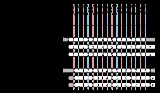
Example: SPI bus timing
The timing diagram example on the right describes the Serial Peripheral Interface (SPI) BusSerial Peripheral Interface Bus
The Serial Peripheral Interface Bus or SPI bus is a synchronous serial data link standard named by Motorola that operates in full duplex mode. Devices communicate in master/slave mode where the master device initiates the data frame. Multiple slave devices are allowed with individual slave select ...
.
Most SPI master nodes have the ability to set the clock polarity (CPOL) and clock phase (CPHA) with respect to the data.
This timing diagram shows the clock for both values of CPOL as well as the values for the two data lines (MISO & MOSI) for each value of CPHA.
Note that when CPHA=1 then the data is delayed by one-half clock cycle.
SPI operates in the following way:
- The master determines an appropriate CPOL & CPHA value
- The master pulls down the slave select (SS) line for a specific slave chip
- The master clocks SCK at a specific frequency
- During each of the 8 clock cycles the transfer is full duplex:
- The master writes on the MOSI line and reads the MISO line
- The slave writes on the MISO line and reads the MOSI line
- When finished the master can continue with another byteByteThe byte is a unit of digital information in computing and telecommunications that most commonly consists of eight bits. Historically, a byte was the number of bits used to encode a single character of text in a computer and for this reason it is the basic addressable element in many computer...
transfer or pull SS high to end the transfer
When a slave's SS line is high then both of its MISO and MOSI line should be high impedance so to avoid disrupting a transfer to a different slave.
Prior to SS being pulled low, the MISO & MOSI lines are indicated with a "z" for high impedance.
Also prior to the SS being pulled low the "cycle #" row is meaningless and is shown greyed-out.
Note that for CPHA=1 the MISO & MOSI lines are undefined until after the first clock edge and are also shown greyed-out before that.
A more typical timing diagram has just a single clock and numerous data lines