

Ballistic Conduction in Single-Walled Carbon Nanotubes
Encyclopedia
Conductance Quantization and Landauer Formula
Conduction in single-walled carbon nanotubeCarbon nanotube
Carbon nanotubes are allotropes of carbon with a cylindrical nanostructure. Nanotubes have been constructed with length-to-diameter ratio of up to 132,000,000:1, significantly larger than for any other material...
s is quantized due to their one-dimensionality and the number of allowed electronic states is limited, if compared to bulk graphite. The nanotubes behave consequently as quantum wire
Quantum wire
In condensed matter physics, a quantum wire is an electrically conducting wire, in which quantum effects are affecting transport properties. Due to the quantum confinement of conduction electrons in the transverse direction of the wire, their transverse energy is quantized into a series of...
s and charge carriers are transmitted through discrete conduction channels. This conduction mechanism can be either ballistic or diffusive in nature, or based on tunneling. When ballistically conducted, the electrons travel through the nanotubes channel without experiencing scattering
Carrier scattering
Defect types include atom vacancies, adatoms, steps, and kinks which occur most frequently at surfaces due to finite material size causing crystal discontinuity. What all types of defects have in common, whether they be surface or bulk, is that they produce dangling bonds which have specific...
due to impurities, local defects or lattice vibrations. As a result, the electrons encounter no resistance and no energy dissipation occurs in the conduction channel.
In order to estimate the current in the carbon nanotube channel, the Landauer formula can be applied, which considers a one-dimensional channel, connected to two contacts – source and drain.
Assuming no scattering and ideal (transparent) contacts, the conductance of the one-dimensional system is given by G = G0NT, where T is the probability that an electron will be transmitted along the channel, N is the number of the channels available for transport, and G0 is the conductance quantum
Conductance quantum
The conductance quantum is the quantized unit of conductance. It is defined as G0 = 2e2/h = ≈ Ω−1. It appears when measuring the conductance of a quantum point contact....
2e2/h = 12.9kΩ−1. Perfect contacts, with reflection R = 0, and no back scattering along the channel result in transmission probability T = 1 and the conductance of the system becomes G = (2e2/h) N. Thus each channel contributes 2G0 to the total conductance.
For metallic armchair nanotubes, there are two subbands, which cross the Fermi level
Fermi level
The Fermi level is a hypothetical level of potential energy for an electron inside a crystalline solid. Occupying such a level would give an electron a potential energy \epsilon equal to its chemical potential \mu as they both appear in the Fermi-Dirac distribution function,which...
, and for semiconducting nanotubes – bands which don’t cross the Fermi level. Thus there are two conducting channels and each band accommodates two electrons of opposite spin. Thus the value of the conductance is G = 4G0 = 25.8 kΩ−1.
In a non-ideal system, T in the Landauer formula is replaced by the sum of the transmission probabilities for each conduction channel. When the value of the conductance for the above example approaches the ideal value of 4G0, the conduction along the channel is said to be ballistic. This happens when the scattering length in the nanotube is much greater than the distance between the contacts.
If a carbon nanotube is a ballistic conductor, but the contacts are nontransparent, the transmission probability, T, is reduced by back-scattering in the contacts. If the contacts are perfect, the reduced T is due to back-scattering along the nanotube only.
When the resistance measured at the contacts is high, one can infer the presence of Coulomb blockade
Coulomb blockade
In physics, a Coulomb blockade , named after Charles-Augustin de Coulomb's electrical force, is the increased resistance at small bias voltages of an electronic device comprising at least one low-capacitance tunnel junction. Because of the CB, the resistances of devices are not constant at low bias...
and Luttinger liquid
Luttinger liquid
A Tomonaga-Luttinger liquid, more often referred to as simply a Luttinger liquid, is a theoretical model describing interacting electrons in a one-dimensional conductor...
behavior for different temperatures. Low contact resistance is a prerequisite for investigating conduction phenomena in CNTs in the high transmission regime.
Quantum Interference
When the size of the CNT device scales with the electron coherence length, important in the ballistic conduction regime in CNTs becomes the interference pattern arising when measuring the differential conductance as a function of the gate voltage. This pattern is due to the quantum interference of multiply reflected electrons in the CNT channel. Effectively, this corresponds to a Fabry-Perot resonator, where the nanotube acts as a coherent waveguide and the resonant cavity is formed between the two CNT-electrode interfaces. Phase coherent transport, electron interference, and localized states have been observed in the form of fluctuations in the conductance as a function of the Fermi energy.
Phase coherent electrons give rise to the observed interference effect at low temperatures. Coherence then corresponds to a decrease in the occupation numbers of phonon modes and a decreased rate of inelastic scattering. Correspondingly, increased conduction is reported for low temperatures.
Ballistic Conduction in CNT Field-Effect Transistors
CNT FETs exhibit four regimes of charge transport:- ohmic contact ballistic
- ohmic contact diffusive
- Schottky barrierSchottky barrierA Schottky barrier, named after Walter H. Schottky, is a potential barrier formed at a metal–semiconductor junction which has rectifying characteristics, suitable for use as a diode...
ballistic - Schottky barrier diffusive
Ohmic contact
Ohmic contact
An ohmic contact is a region on a semiconductor device that has been prepared so that the current-voltage curve of the device is linear and symmetric. If the I-V characteristic is non-linear and asymmetric, the contact is not ohmic, but is a blocking or Schottky contact...
s require no scattering as the charge carriers are transported through the channel, i.e. the length of the CNT should be much smaller than the mean free path
Inelastic mean free path
The inelastic mean free path is an index of how far an electron can travel through a solid before losing energy.If a monochromatic primary beam of electrons is incident on a solid surface, the majority of incident electrons lose their energy because they interact strongly with matter, leading to...
(L<< lm). The opposite is valid for diffusive transport.
In semiconducting CNTs at room temperature and for low energies, the mean free path is determined by the electron scattering from acoustic phonons, which results in lm ≈ 0.5μm. In order to satisfy the conditions for ballistic transport, one has to take care of the channel length and the properties of the contacts, while the geometry of the device could be any top-gated doped CNT FET.
Ballistic transport in a CNT FET takes place when the length of the conducting channel is much smaller than the mean free path of the charge carrier, lm.
Ballistic conduction in Ohmic Contact FETs
Ohmic i.e. transparent contacts are most favorable for an optimized current flow in a FET.In order to derive the current-voltage (I-V) characteristics for a ballistic CNT FET, one can start with Planck's postulate, which relates the energy of the i-th state to its frequency:
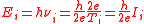
The total current for a many-state system is then the sum over the energy of each state multiplied by the occupation probability function, in this case the Fermi-Dirac statistics
Fermi-Dirac statistics
Fermi–Dirac statistics is a part of the science of physics that describes the energies of single particles in a system comprising many identical particles that obey the Pauli Exclusion Principle...
:
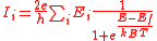
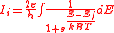
For a system with dense states, the discrete sum can be approximated by an integral:
In CNT FETs, the charge carriers move either left (negative velocity) or right (positive velocity) and the resulting net current is called drain current. The source potential controls the right-moving, and the drain potential - the left moving carriers and if the source potential is set to zero, the Fermi energy at the drain subsequently decreases to yield positive drain voltage. The total drain current is computed as a sum of all contributing subbands in the semiconductor CNT, but given the low voltages used with nanoscale electronics, higher subbands can be effectively ignored and the drain current is given only by the contribution of the first subband:

where
and
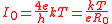
 is the quantum resistance.
The expression for
 gives the ballistic current dependence on the voltage in a CNT FET with ideal contacts.
Ballistic conduction with Optical Phonon Scattering
Ideally, ballistic transport in CNT FETs requires no scattering from optical or acoustic phonons, however the analytical model yields only partial agreement with experimental data. Thus, one needs to consider a mechanism, which would improve the agreement and recalibrate the definition of ballistic conduction in CNTs. Partially ballistic transport is modeled to involve optical phonon scattering. Scattering of electrons by optical phonons in carbon nanotube channels has two requirements:- The traveled length in the conduction channel between source and drain has to be greater than the optical phonon mean free path
- The electron energy has to be greater than the critical optical phonon emission energy
Schottky barrier Ballistic conduction
CNT FETs with Schottky contacts are easier to fabricate than those with ohmic contacts. In these transistors, the gate voltage controls the thickness of the barrier, and the drain voltage can lower the barrier height at the drain electrode. Quantum tunneling of the electrons through the barrier should also be taken into account here. In order to understand the charge conduction in Schottky barrier CNT FETs, we need to study the band schemes under different bias conditions (Fig 2):- the net current is a result of electrons tunneling from the source and electrons tunneling from the drain
- ON-state: electrons tunneling from the source
- OFF-state: holes tunneling from the drain
Thus, the Schottky barrier CNT FET is effectively an ambipolar transistor, since the ON electron current is opposed by an OFF hole current, which flows at values smaller than the critical gate voltage value.
From the band diagrams, one can deduce the
 characteristics of the Schottky CNT FETs. Starting at the OFF state, there is hole current, which gradually decreases as the gate voltage is increased until it is opposed with equal strength by the electron current coming from the source. Above the critical gate voltage in the ON state, the electron current prevails and reaches a maximum at
  and the
  curve will roughly have a V-shape.